KB: Fit Document Zooms Too Far and Does Not Center on PCB Board Shape
Updated: April 27, 2026
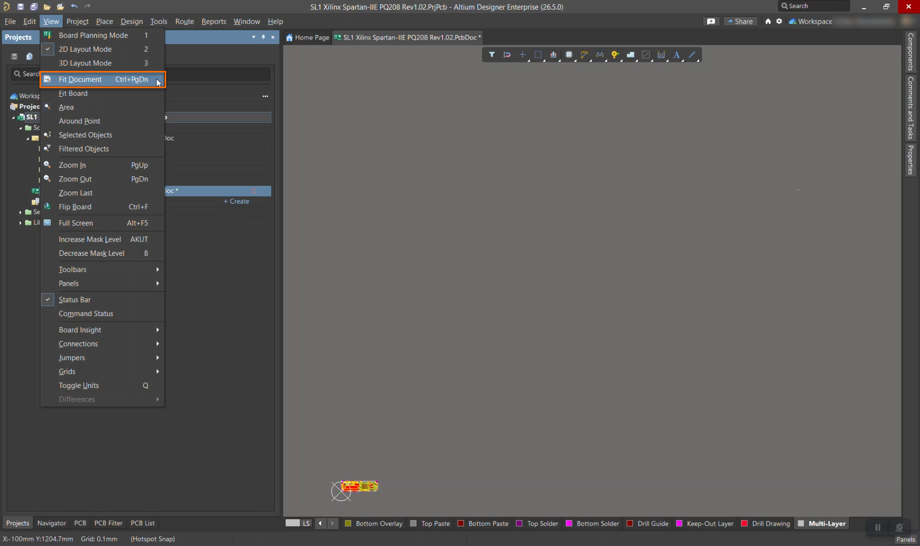
The Fit Document command (View » Fit Document, Ctrl+PgDn) in an Altium Designer PCB document fits the view to the full extents of all objects in the design. If objects exist far outside the intended board area, the command zooms out excessively, making the board shape appear missing or extremely small. This commonly occurs after importing DXF outlines or accidentally placing objects well away from the board shape. Identifying and removing these unintended distant objects restores the expected behaviour of the Fit Document command and allows the PCB board shape to be displayed correctly.
Solution Details
Board shape not visible after Fit Document
After using Fit Document command (View » Fit Document, Ctrl+PgDn), the PCB view zooms far out and the board shape cannot be easily seen. The PCB document opens normally, but the visible area includes a large empty space, giving the impression that the board outline is missing or incorrect.
All object extents affect the view
The Fit Document command fits the view to the extents of all objects in the PCB document, not only the board shape. If any primitives, mechanical objects, or imported geometry are located far from the board outline, they expand the document extents and force the view to zoom out.
Remove unintended objects outside board area
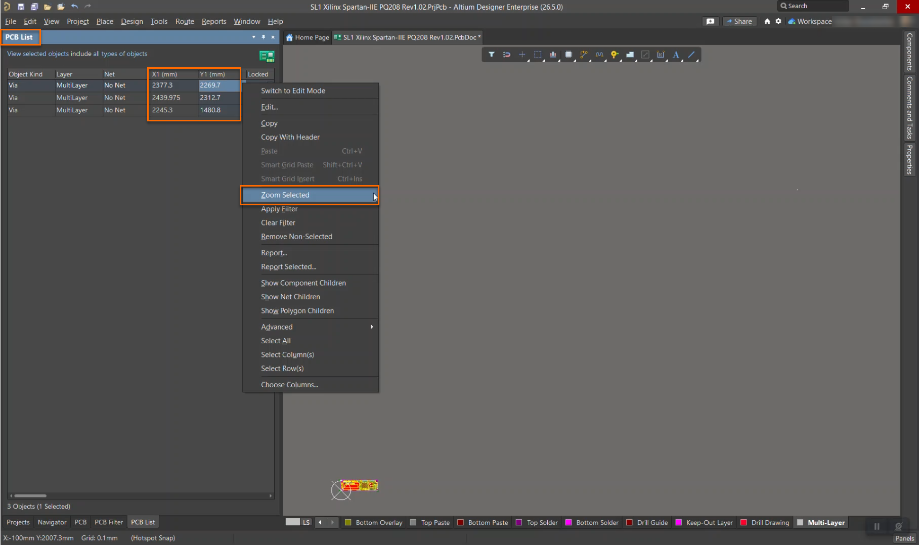
- Use the PCB List panel as part of Altium Designer's global editing and inspection workflow to locate, review, and interrogate objects that are difficult to find graphically.
- Identify PCB objects that exist outside the intended board area.
- Review whether these objects are intentional or required.
- Delete unnecessary objects to reduce the document extents.
Select and remove distant objects
- Open the PCB document.
- Go to View Configuration panel and enable all layers.
- Ensure Single Layer Mode is turned off.
- In the selection filter, ensure All Objects are enabled.
- Go to Edit » Select » Outside Area.
- Draw a rectangle that encloses all valid PCB objects near the board shape.
- Check the Properties panel to confirm that objects are selected.
- Open Panels » PCB List and enable Selected Objects.
- Review the selected objects and identify any that are far from the board shape.
- Use Zoom Selected to inspect objects if required.
- Delete unwanted objects using Edit » Delete.