
KB: How to Identify Mirrored Components in a PCB Design
Updated: August 25, 2026
 Altium Designer
In PCB designs, mirrored components may require special attention during review or manufacturing. However, there is currently no direct X/Y mirror indication available in the component Properties panel, and the PCB List panel does not provide a column that identifies mirrored components. Because mirror state is not exposed as a searchable component attribute, users must use alternative methods to identify affected parts. Newer software versions provide a PCB Health Check that can identify mirrored components, while older versions require a workaround that uses the PCB Filter panel to locate mirrored text objects and then the PCB List panel to determine the associated components. This article explains the limitation and provides the available methods for identifying mirrored components.
Solution Details
Mirror Status Not Directly Visible
There is no X/Y mirror indicator exposed in the component Properties panel. Additionally, the PCB List panel does not include a column that indicates whether a component has been mirrored, making direct identification difficult.
Component Mirror State Is Not Searchable
Mirror information is not available as a searchable component property. As a result, users cannot directly query or filter components based on their mirror state and must instead rely on indirect identification methods. PCB Health Checks are designed to identify potentially problematic PCB conditions that may not be reported through standard DRC checks, including conditions that can impact manufacturing, outputs, MCAD collaboration, or overall design quality.
Select the Appropriate Detection Method
- Method 1: Use the built-in PCB Health Check to identify mirrored components.
- Method 2: Use the PCB Filter panel to locate mirrored text objects and then determine the associated components through the PCB List panel.
Identify Mirrored Components Step by Step
Method 1: PCB Health Check
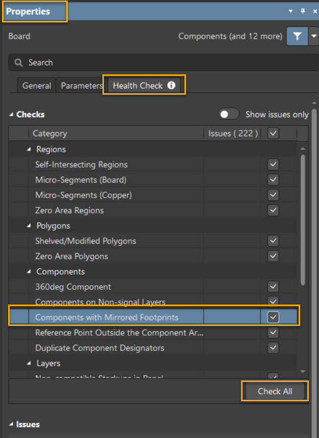
- Open the PCB document.
- Ensure that no object is currently selected.
- Open the Properties panel and access the Health Check section.
- Run the applicable health check and review any mirrored component results that are reported.
Notes:
- Availability of PCB Health Check functionality may depend on the product configuration, license, and software version.
- The Components with Mirrored Footprints health check does not simply report every mirrored component present in the PCB. Instead, it detects mirroring-related differences between a placed component footprint and the corresponding footprint in the source library. When a fix is applied, only mirroring-related elements such as pins, overlays, and 3D bodies are considered. Other footprint modifications, including rotation changes, are not evaluated or modified by this check. Therefore, the results should not be interpreted as a complete list of all mirrored components in the design.
Method 2: PCB Filter
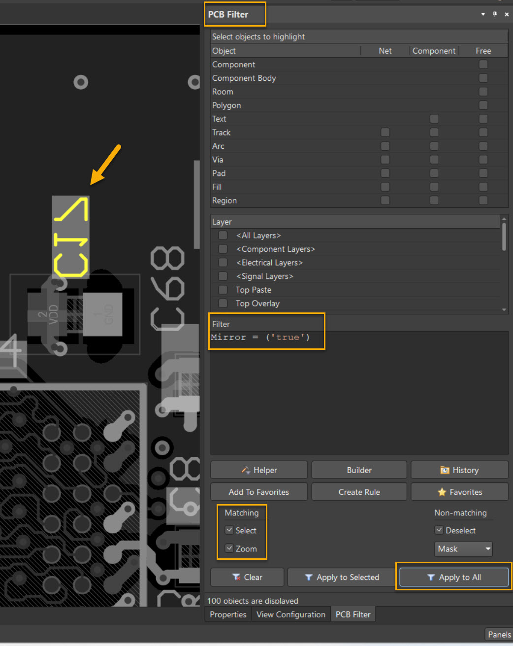
- Open PCB Filter from Panels » PCB Filter.
- Under Matching, enable Select.
- Set the filter condition to Mirror = ('true').
- Select Apply to All to select all mirrored text objects.
- Open PCB List from Panels » PCB List.
- Change the list scope to Selected Objects and include all object types.
- Review the resulting list to identify the associated components.
Notes:
- This only works if the component text is mirrored.
- By default, text is mirrored with the component even when the component is rotated.
- If a component was mirrored and the text was later individually mirrored back, it will not be detected using this method.