
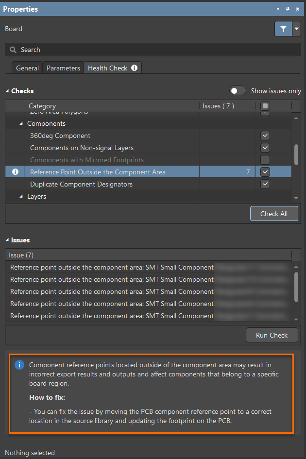
KB: PCB Health Check Monitor - Reference Point Outside the Component Area
Solution Details
Warning appears on specific components
The PCB Health Check Monitor reports the warning Reference Point Outside the Component Area for certain components rather than the entire design. The PCB layout may look correct, but the repeated warning can raise concerns about potential errors in generated outputs, exports, or manufacturing data.
Origin no longer aligned with footprint area
This warning occurs when the component origin (reference point) is located outside the actual component area. A common scenario involves single‑pad components where the pad was moved independently instead of moving the entire component. As a result, the pad no longer aligns with the component’s reference point. Even though the footprint may appear correct on the PCB, the PCB Health Check Monitor detects this internal inconsistency and flags it because it can affect exports, outputs, and components associated with specific board regions.
Correct the reference point at the source
- Ensure the component reference point is located within the component area and aligned with the pad.
- Apply the correction in the source library and then update the footprint on the PCB.
Note (as shown in the PCB Health Check Monitor panel): Component reference points located outside of the component area may result in incorrect export results and outputs and can affect components that belong to a specific board region.
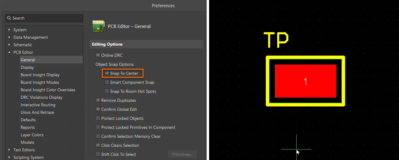
Verify and realign the component origin
- Enable Snap To Center in the PCB Editor Preferences and move or drag the component.
- Identify whether the pad has been moved independently of the component.
- Open the affected component in the source library.
- Check whether the component origin lies outside the component area.
- If required, use Edit » Set Reference to move the origin inside the component area.
- Save the updated library component.
- Update the PCB with the corrected library footprint.
- Re‑run the PCB Health Check Monitor to confirm the issue is resolved.
Additional Notes
The component reference point is used internally for snapping and placement. Enabling Snap To Center is the most practical way to identify its location, as the component will be grabbed and moved directly from the reference point during placement or dragging.
References
- PCB Health Check Monitor documentation
- For issues where components cannot be moved or snap back unexpectedly due to origin or coordinate constraints, refer to the following Knowledge Base article:
KB: Unable to Move Specific Components in the PCB Editor