
KB: Signal to plane layer conversion - Preserving polygons
Updated: November 18, 2025
When converting a signal layer to a plane layer in PCB design, polygons with different net name assignments are lost due to the fundamental differences in layer types and artwork handling. Signal layers support polygon-based routing, while plane layers require split planes with defined net assignments, which are not automatically preserved during conversion. Although there is no direct method to retain these polygons, users can apply workarounds such as manually recreating split planes, exporting and re-importing polygons via DXF, or using a temporary layer to explode polygons into free primitives and reassign them to the plane layer. These methods help maintain design integrity and net connectivity despite the limitations of the layer conversion process.
Solution Details
Issue Overview
When converting a signal layer to a plane layer, all polygons with different net name assignments are lost. This issue arises during layer type changes in PCB design workflows, where users expect the polygons to be retained or converted into split planes.
Why polygons are lost during the conversion
Signal and plane layers are treated as different artwork types in PCB design tools. The conversion process does not support direct retention of polygons from signal layers because plane layers require split planes with net assignments, which are not automatically derived from signal layer polygons.
Available workarounds
There is no straightforward way to convert existing polygons into split planes. However, users can apply one of the following workarounds:
- Manually recreate the split planes in the plane layer.
- Export polygons as DXF and re-import them into a mechanical layer, then move outlines to the plane layer.
- Use a temporary layer to hold polygons, explode them into free primitives, and assign nets manually.
How to apply the workarounds
Option 1: Manual Recreation
- Note the net assignments and shapes of the original polygons.
- Recreate each split plane manually in the plane layer using the same outlines and net names.
Option 2: DXF Export/Import
- Select all the polygons.
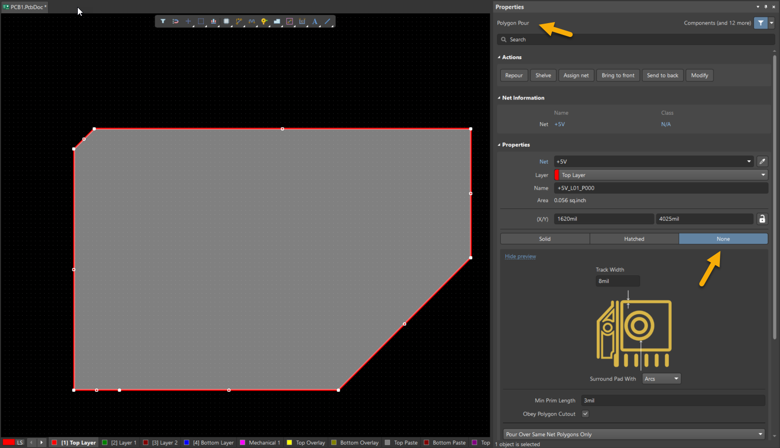
- Open the Properties Panel and Change the Polygon fill mode to "None".
- Export the polygons from the signal layer as a DXF file.
- Import the DXF into a mechanical layer.
- Select the outlines of each polygon.
- Move the polygon outlines to the plane layer using the Properties Panel.
- Assign the appropriate nets to each split plane.
Option 3: Temporary Layer and Explode
- Create a temporary layer in the stackup.
- Move the polygons from the signal layer to the temporary layer.
- Change the signal layer to a plane layer.
- Select all the polygons in the temporary layer.
- Open the properties panel and Change the Polygon fill mode to "None"
- Move the Polygon outlines to the plane layer.
- Assign nets to the split planes manually.
Additional Notes
- These workarounds are manual and may require careful attention to net assignments to avoid connectivity issues.
- Always verify net connectivity after applying any workaround.