
KB: KeysightのSI Analyzerを使用して簡単な伝送線路シミュレーションを作成する方法
Updated: 7月 01, 2026
 Altium Designer
この記事では、Altium Designer内のSI Analyzer by Keysightを使用して、シンプルな伝送線路シミュレーションを作成する手順を説明します。目的は、2つのSMAコネクタ間を接続する伝送線路の特性インピーダンスが、指定された目標値の許容範囲内に収まっていることを確認することです。手順には、回路図とPCBレイアウトの作成、インピーダンスプロファイルの設定、制約の定義、シミュレーション解析が含まれます。SI AnalyzerはAltium Designerに統合されており、レイアウト前とレイアウト後の両方のシグナルインテグリティ解析に対応しています。
ソリューションの詳細
伝送線路のインピーダンス検証のシナリオと範囲
目的は、2つのSMAコネクタ間に、指定した長さと目標インピーダンスを持つ伝送線路を設計し、Altium Designer内のSI Analyzerを使用して、インピーダンスが許容範囲内に収まっていることを検証することです。
PCB設計におけるインピーダンス不整合の原因
高速PCB設計におけるインピーダンス不整合は、通常、不適切な配線幅、スタックアップ定義の誤り、または制約定義の欠落によって発生します。これらの問題は、信号の反射や劣化を引き起こし、全体的な性能の低下につながる可能性があります。SI Analyzerなどのツールを使用して適切に検証しなければ、設計サイクルの後半まで問題が発見されないことがあります。
インピーダンス制約を定義する方法
機能の利用可否:利用できる機能は、お使いのAltiumソリューションによって異なります。対象となるのは、 Altium Develop、Altium Agileの各エディション(Agile TeamsまたはAgile Enterprise)、またはAltium Designer(有効な契約期間内)です。
シミュレーションと検証の手順
Create the project and schematic Altium Designer で新しいプロジェクトを作成します。- 回路図(
*.SchDoc*.PcbDoc - 必要に応じて、プロジェクト作成時に制約管理を有効にします。
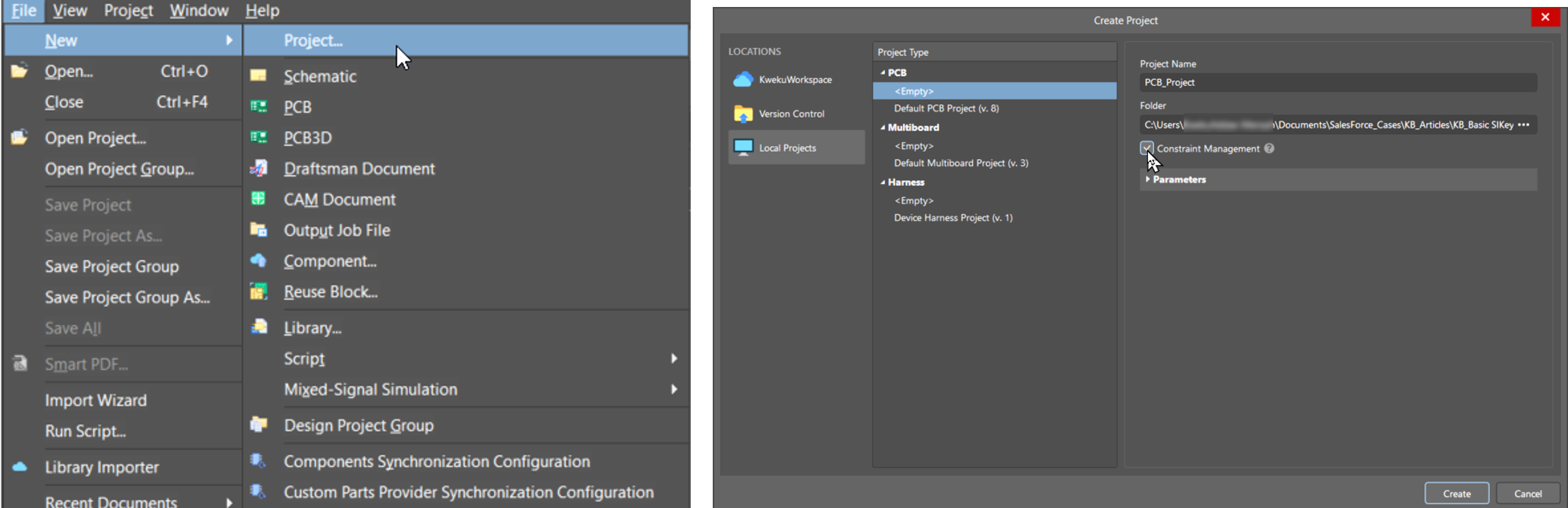
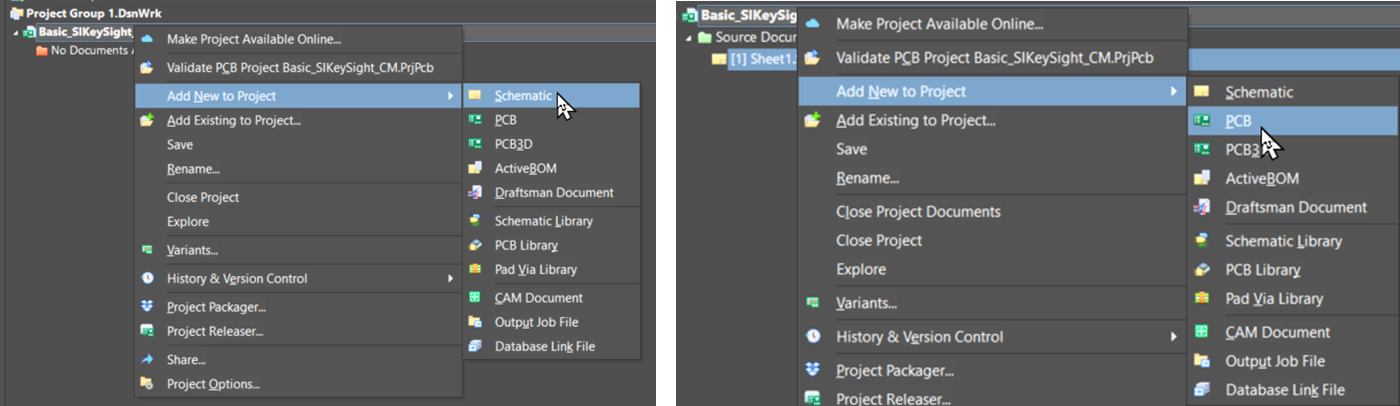
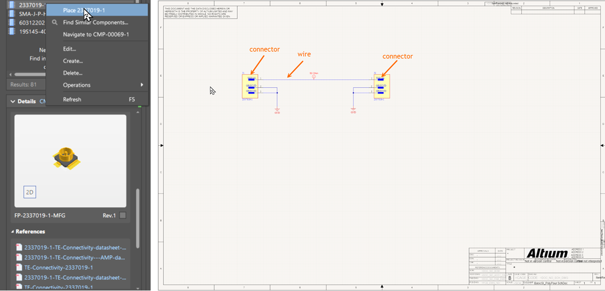
Place SMA connectors - ライブラリ(ローカルまたはAltium 365 Workspace)からSMAコネクタを選択します。
- 回路図に2つのコネクタを配置します。
- 信号ピン同士をワイヤで接続します。
- その他のすべてのピンをGNDに接続します。
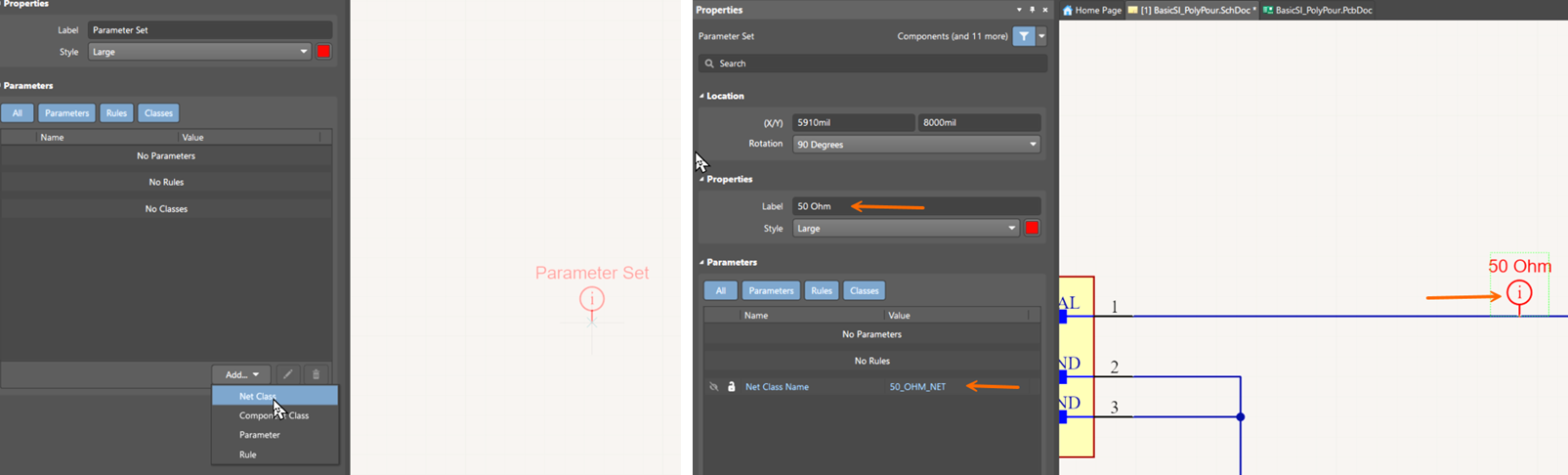
Define impedance constraints Design Directives Method: - 目標インピーダンス用のパラメータセットを作成します。
- ネットクラス名を割り当て、信号ワイヤに関連付けます。
Constraint Manager Method: - 回路図から
Constraint Manager を開きます。 - 新しいクラス(例:
50OhmLine )を追加し、対象のネットを割り当てます。 - PhysicalタブでPreferred Widthを設定します。
- Trace Widthウィンドウでインピーダンスプロファイルを選択します。
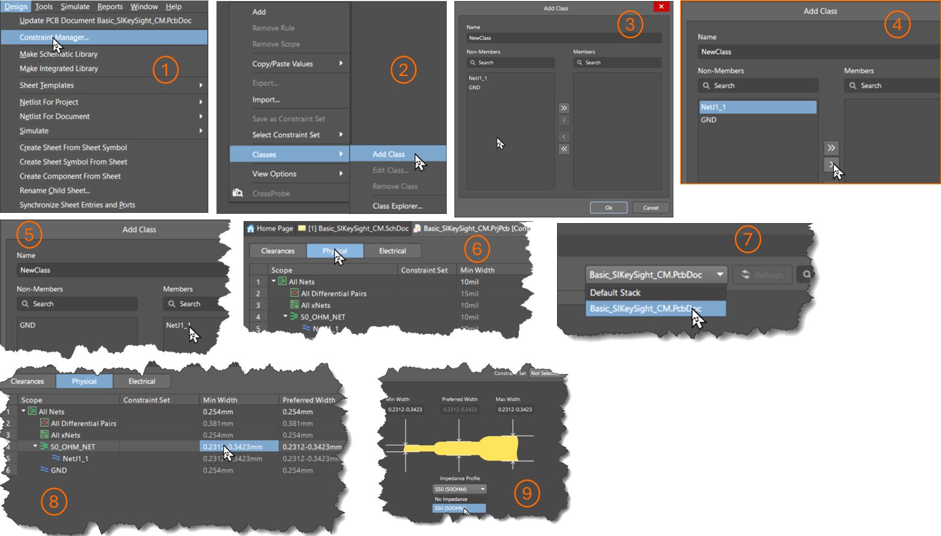
注:この手順を完了する前に、スタックアップとインピーダンスプロファイルを作成しておく必要があります。
- 回路図から
Create stack-up and impedance profile - 適切な誘電体材料、厚さ、銅箔重量を使用して、
*.PcbDoc - Altiumのインピーダンス計算機または外部ツールを使用して、配線幅を決定します。
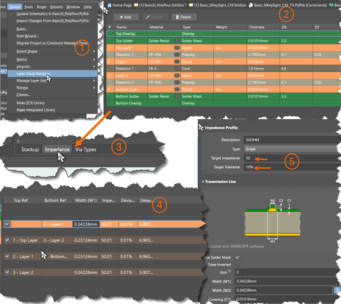
- 適切な誘電体材料、厚さ、銅箔重量を使用して、
Update PCB and complete layout Generate ECO を使用してPCBを更新します。- 必要な間隔を空けて、基板外形上にコネクタを配置します。
- プレーンとポリゴンポアをGNDネットに割り当てます。
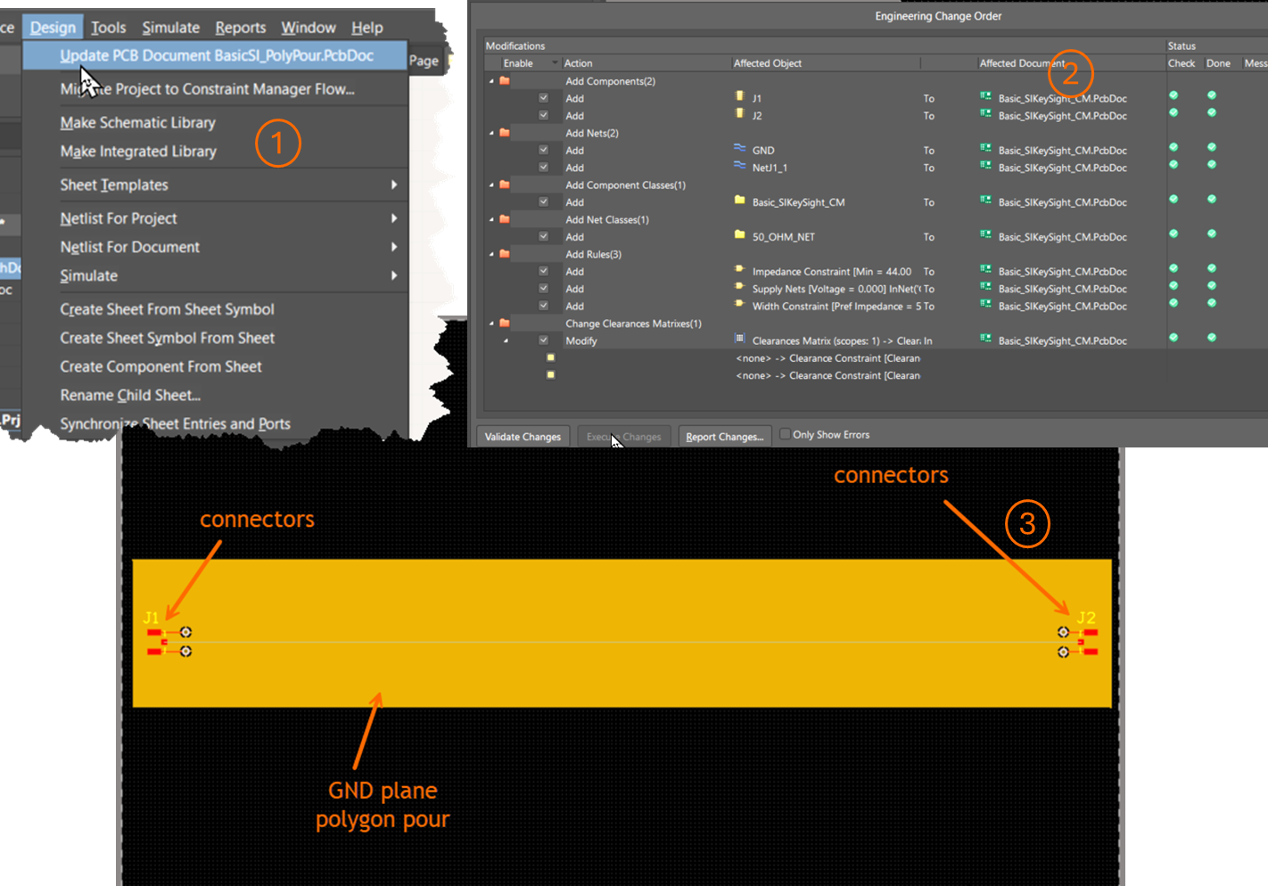
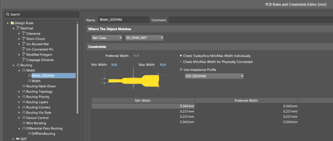
Apply design rules and validate layout - インピーダンスプロファイルまたは外部での計算結果を使用して、配線幅のデザインルールを作成します。
- Altium Designerは、
PCB Rules and Constraints Editor またはConstraint Manager を介して、インタラクティブ配線中にインピーダンスプロファイルを適用します。 - グランドパッドと配線を適切に接続します。
- DRCを実行してエラーを確認します。
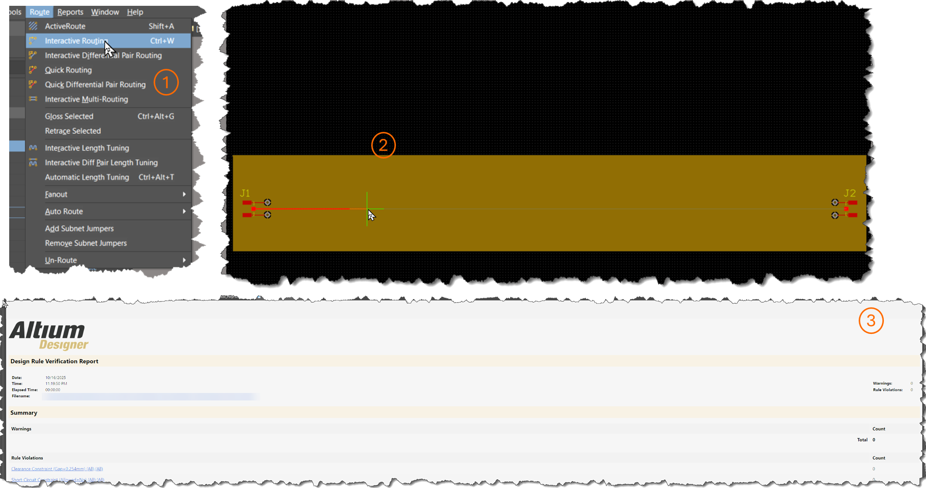
Run SI simulation and verify results - Altium Designerに統合されている
SI Analyzer by Keysight を読み込みます。 Manage Specifications でインピーダンス仕様を作成します(挿入損失、反射損失、遅延の設定は省略できます)。Manage Nets で、対象のネットまたはクラスに仕様を割り当てます。Analyze をクリックします。- インピーダンスが目標値に対する許容範囲内に収まっていることを確認します。
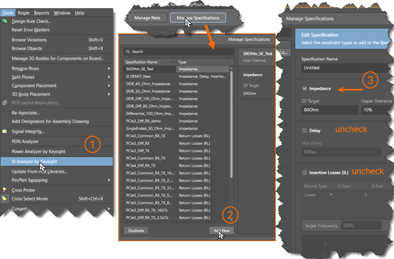
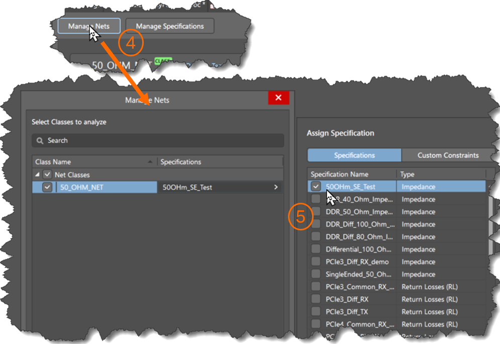
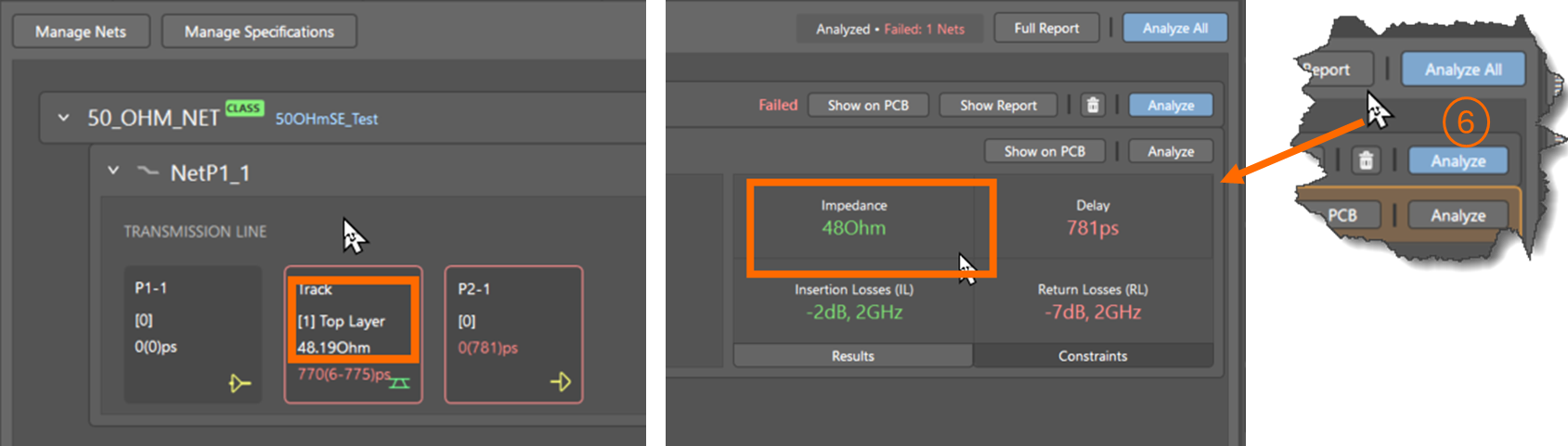
- Altium Designerに統合されている
補足事項
- 挿入損失、反射損失、遅延の仕様が定義されていない場合、SI Analyzerはデフォルト値に基づいて不合格と判定することがあります。
- Constraint Managerでわかりやすく表示されるように、意味のあるクラス名(例:
50OhmLine )を使用してください。 - 複雑なスタックアップでは、外部のインピーダンス計算機を使用することで、より柔軟に対応できる場合があります。
- SI Analyzerは、Altium Designerの回路図環境またはPCBレイアウト環境から直接起動できます。
参考資料
- SI Analyzer by Keysight – SI Analyzer by Keysight拡張機能の機能、セットアップ、ライセンス要件を紹介します。
- レイヤースタックの定義 – インピーダンス制御配線に不可欠なPCBレイヤースタックの定義方法と設定方法を説明します。
- シグナルインテグリティ解析に向けた設計の準備 – シグナルインテグリティ解析を実行する前に必要な前提条件と準備手順を説明します。
- KB:レイヤースタックで計算された伝送線路のインピーダンスの検証 – Layer Stack Managerによるインピーダンスの計算結果を検証する方法と、その結果が外部計算機と異なる場合がある理由を説明します。
 AI で翻訳