
KB: Large Component Selection Bounding Box
Updated: 12月 11, 2025
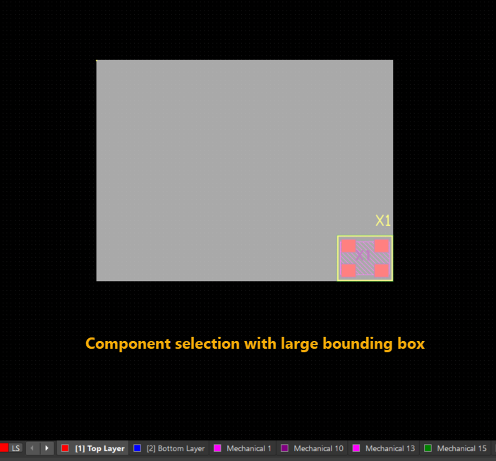
A component in Altium PCB Editor may appear to have an unusually large selection bounding box. This occurs because the selection box in Graphics mode includes all geometries associated with the component, such as objects on the Courtyard layer, Silkscreen, 3D body objects, and Copper layers. If any graphical object is placed far away from the component center—either accidentally during footprint creation or due to unlocked primitives being moved in the PCB—the bounding box expands to include that object. Resolving this issue involves updating the footprint from the library or manually removing misplaced objects from the footprint.
Solution Details
Problem Description
A particular component is getting selected with a large bounding box in PCB Editor, making it difficult to work with or align accurately.
Why Does the Bounding Box Expand?
When selecting components, the bounding box includes all geometries detected on the Courtyard layer type, Silkscreen, 3D body objects, and Copper layers. If any graphical object is placed away from the component center, the bounding box expands to include it. This often happens when:
- A graphical object (e.g., track or arc) was accidentally placed far from the footprint center during footprint creation.
- Component primitives were unlocked in the PCB and moved unintentionally.
Available Solutions
There are two main solutions:
- Solution 1: Update the footprint from the library or delete the footprint in the PCB and place a new one from the library.
- Solution 2: Open the problematic footprint in the PCB library and remove any misplaced objects.
Step-by-Step Instructions
Solution 1: Replace the Footprint
- Update the footprint from the library using Tools » Update PCB from Library.
- Alternatively, delete the footprint in the PCB and place a new footprint from the library.
Solution 2: Remove Misplaced Objects
- Open the problematic footprint in the PCB library.
- Go to Edit » Select » Outside Area.
- Draw a rectangle around the footprint objects. This will highlight any objects placed away from the footprint center.
- Delete the highlighted object(s).
- If the object is hidden and not visible:
- Open the Properties Panel and check if any object is selected.
- Use the PCB List Panel to view selected objects.
- Press the Delete key to remove them.
- Update the PCB with the corrected footprint.
Additional Notes
- Always lock component primitives to avoid accidental movement in the PCB.
- Use design rule checks to ensure footprint integrity before placement.