
KB:基板エッジに対する銅プリミティブのクリアランス設定
Solution Details
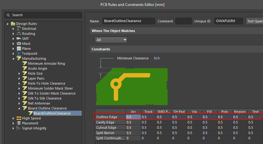
Option 1: Board Outline Clearance
The simpler of the two options may be to specify and enable a Board Outline Clearance rule, from the menu Design » Rules..., expand Manufacturing » Board Outline Clearance, right-click and select New Rule....
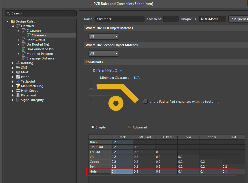
Option 2: Electrical Clearance with Route Tool Path converted as a board cutout
Another option, say, in case you want to have all clearance constraints of electrical objects consolidated under the Electrical Clearance rule category, is to represent Route Tool Path primitives around the board perimeter as "holes" or cutouts on the board.
Because the Route Tool Path is defined on a mechanical layer, "electrical" clearance against these primitives cannot be applied directly. Instead, the Route Tool Path arcs/lines need to be converted to Board Cutouts first, after which a corresponding Electrical Clearance rule can be specified.
To accomplish this, take the following steps:
- Select the primitives in the Rout Tool Path (Typically, the easiest method for this is to select one line in the path, then press TAB to select all connected lines)
- With the primitives from the path selected, go to Tools » Convert » Create Board Cut-out from selected Primitives.
- You will be prompted with a message that an enclosed shape could not be found, asking if you want to create the cutout from the edges. Press Yes to create the cut-out from the edges of your selection.
 AI で翻訳