
KB: Keysight의 SI Analyzer를 사용하여 간단한 전송선 시뮬레이션을 만드는 방법
Updated: July 01, 2026
 Altium Designer
이 문서에서는 Altium Designer 내에서 Keysight의 SI Analyzer를 사용하여 간단한 전송선 시뮬레이션을 생성하는 과정을 설명합니다. 목표는 두 SMA 커넥터 사이에 연결된 전송선의 특성 임피던스가 허용 오차 범위 내에서 지정된 타겟을 충족하는지 확인하는 것입니다. 이 절차에는 Schematic 및 PCB 레이아웃 생성, 임피던스 프로파일 설정, 제약 조건 정의, 시뮬레이션 분석이 포함됩니다. SI Analyzer는 Altium Designer에 통합되어 있으며 레이아웃 전후의 신호 무결성 분석을 모두 지원합니다.
솔루션 상세 정보
전송선 임피던스 검증 시나리오 및 범위
목표는 두 SMA 커넥터 사이에 특정 길이와 타겟 임피던스를 갖는 전송선을 설계하고, Altium Designer의 SI Analyzer를 사용하여 임피던스가 허용 오차 범위 내에 있는지 검증하는 것입니다.
PCB 설계에서 임피던스 불일치가 발생하는 원인
고속 PCB 설계에서 임피던스 불일치는 일반적으로 잘못된 Trace 폭, 부적절한 스택업 정의 또는 제약 조건 정의 누락으로 인해 발생합니다. 이러한 문제는 신호 반사, 신호 품질 저하 및 전반적인 성능 저하를 초래할 수 있습니다. SI Analyzer와 같은 도구로 적절히 검증하지 않으면 설계 주기 후반에 이르러서야 이러한 문제가 발견될 수 있습니다.
임피던스 제약 조건을 정의하는 방법
기능 가용성: 사용할 수 있는 기능은 사용 중인 Altium 솔루션에 따라 달라집니다. 해당 솔루션은 Altium Develop, Altium Agile 에디션(Agile Teams 또는 Agile Enterprise), 또는 Altium Designer(유효한 기간제 라이선스)입니다.
시뮬레이션 및 검증을 위한 단계별 워크플로
Create the project and schematic Altium Designer 에서 새 프로젝트를 시작합니다.- Schematic(
*.SchDoc*.PcbDoc - 필요한 경우 프로젝트 생성 시 제약 조건 관리를 활성화합니다.
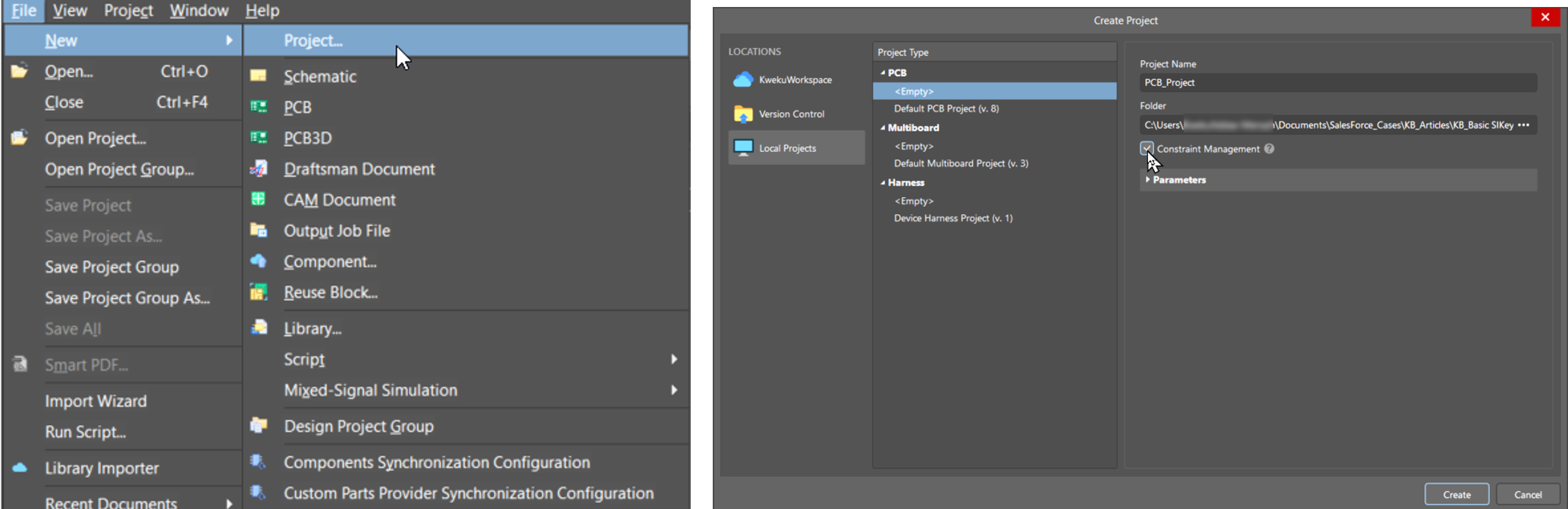
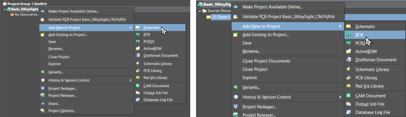
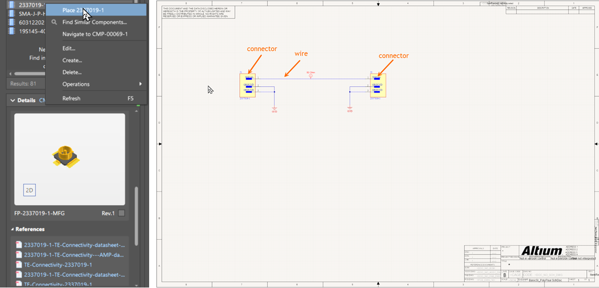
Place SMA connectors - 라이브러리(로컬 또는 Altium 365 워크스페이스)에서 SMA 커넥터를 선택합니다.
- Schematic에 커넥터 두 개를 배치합니다.
- 신호 핀을 와이어로 연결합니다.
- 나머지 모든 핀을 GND에 연결합니다.
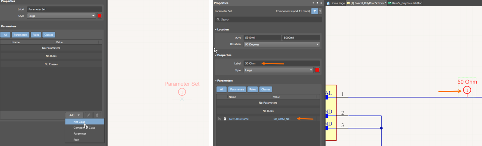
Define impedance constraints Design Directives Method: - 타겟 임피던스에 대한 파라미터 세트를 생성합니다.
- Net 클래스 이름을 지정하고 신호 와이어에 연결합니다.
Constraint Manager Method: - Schematic에서
Constraint Manager 을 엽니다. - 새 클래스(예:
50OhmLine )를 추가하고 타겟 Net을 할당합니다. - Physical 탭에서 기본 설정 폭을 설정합니다.
- Trace 폭 창에서 임피던스 프로파일을 선택합니다.
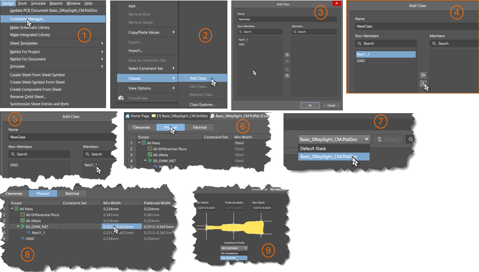
참고: 이 단계를 완료하기 전에 스택업과 임피던스 프로파일을 생성해야 합니다.
- Schematic에서
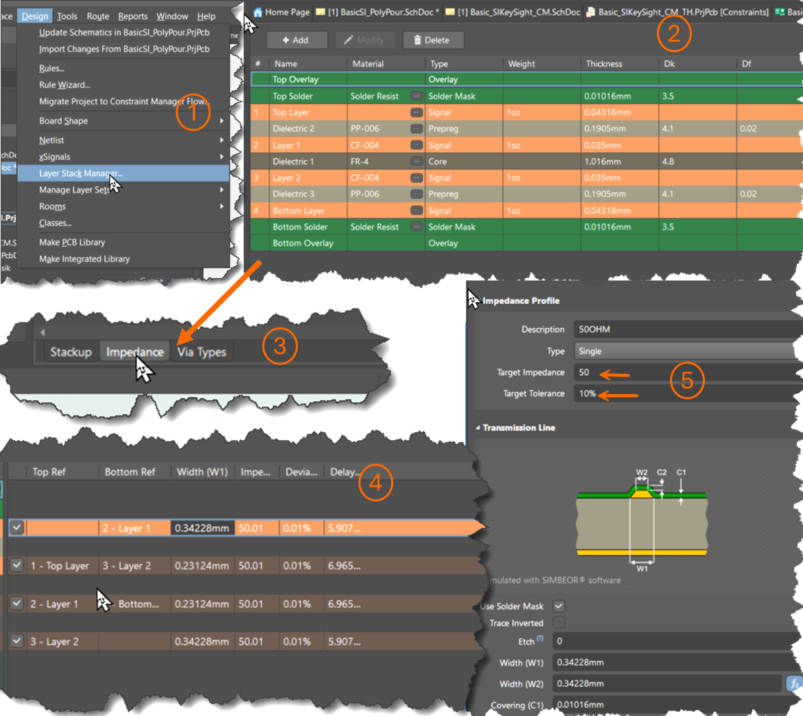
Create stack-up and impedance profile *.PcbDoc- Altium의 임피던스 계산기 또는 외부 도구를 사용하여 Trace 폭을 결정합니다.
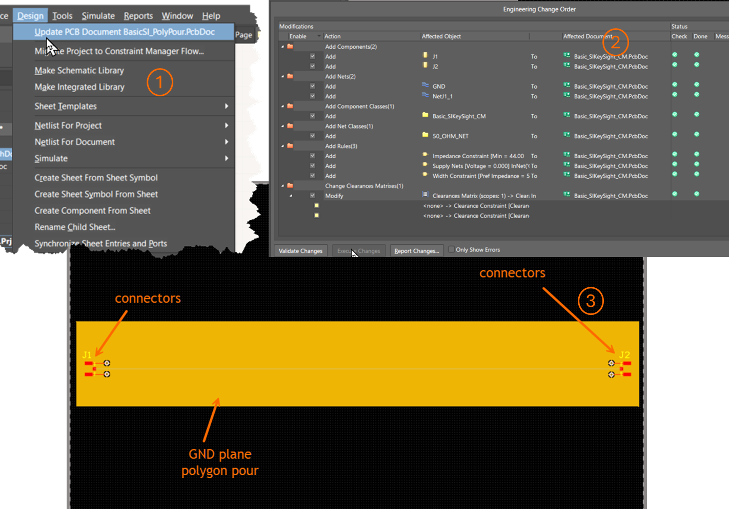
Update PCB and complete layout Generate ECO 을 사용하여 PCB를 업데이트합니다.- 보드 외곽선에 필요한 간격으로 커넥터를 배치합니다.
- 플레인과 폴리곤 푸어를 GND Net에 할당합니다.
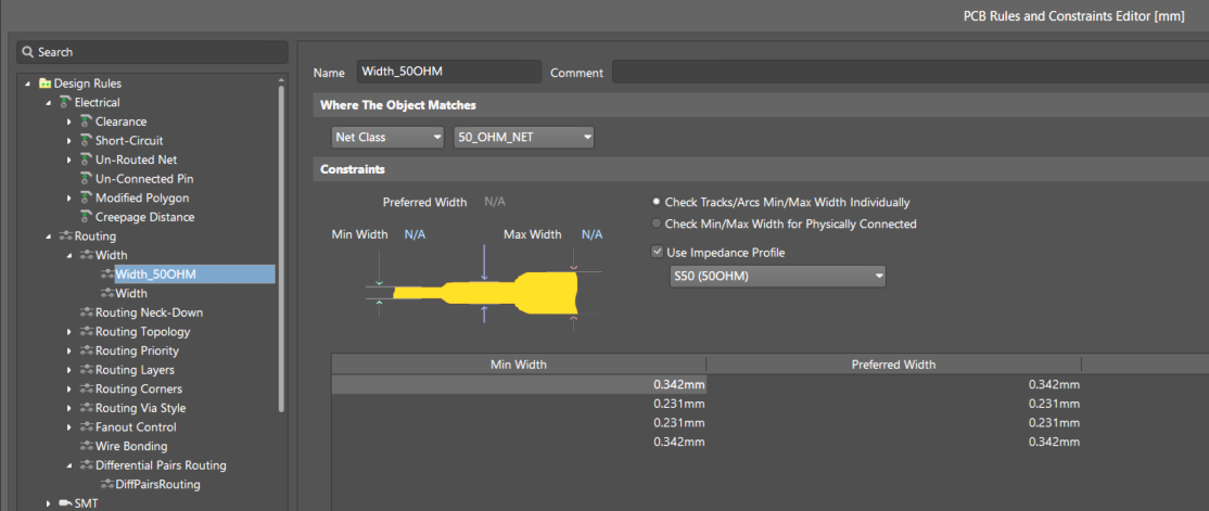
Apply design rules and validate layout - 임피던스 프로파일 또는 외부 계산 결과를 사용하여 Trace 폭에 대한 Design Rule을 생성합니다.
- Altium Designer는 대화형 라우팅 중
PCB Rules and Constraints Editor 또는Constraint Manager 을 통해 임피던스 프로파일을 적용합니다. - 접지 패드와 Trace를 적절히 연결합니다.
- DRC를 실행하여 오류를 확인합니다.
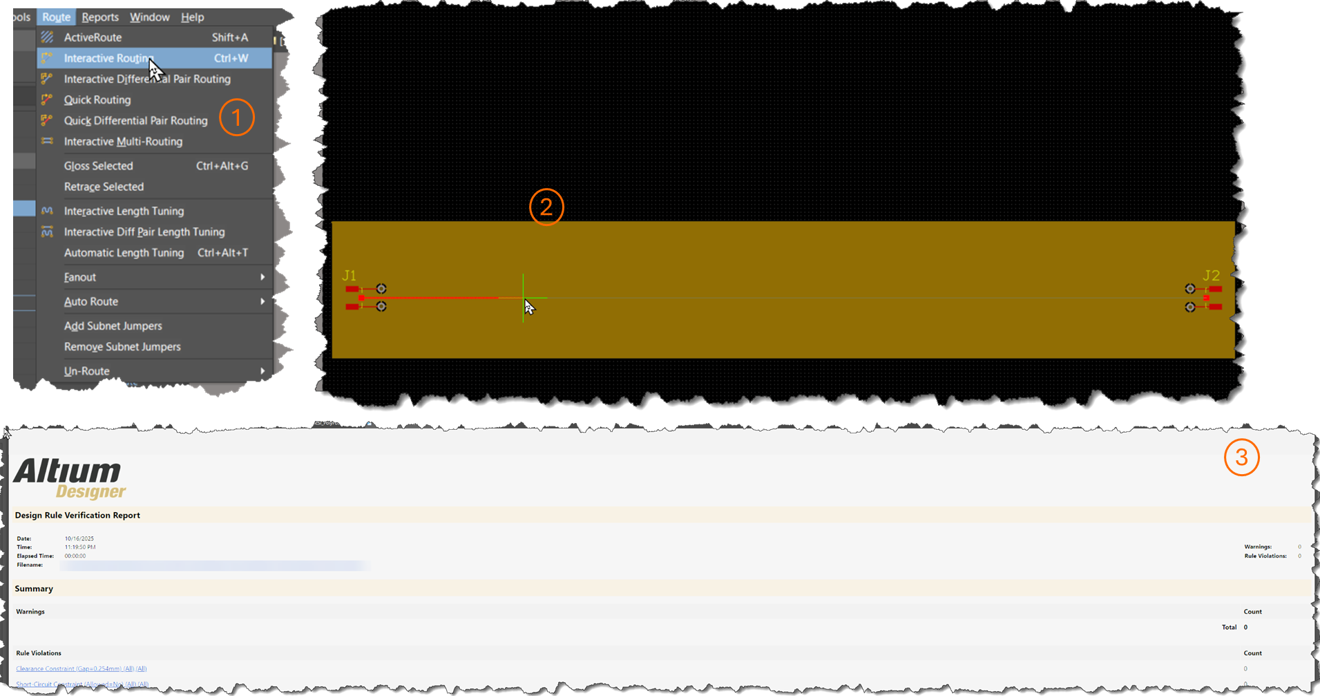
Run SI simulation and verify results - Altium Designer에 통합된
SI Analyzer by Keysight 을 로드합니다. Manage Specifications 에서 임피던스 사양을 생성합니다(삽입 손실, 반사 손실 및 지연은 생략할 수 있음).Manage Nets 에서 타겟 Net 또는 클래스에 해당 사양을 할당합니다.Analyze 을 클릭합니다.- 임피던스가 허용 오차 범위 내에서 타겟 값을 충족하는지 확인합니다.
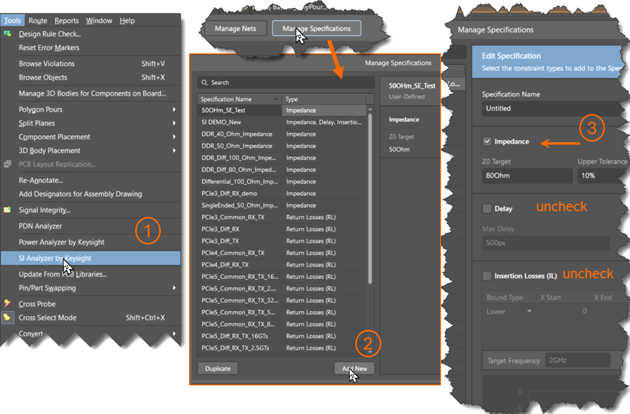
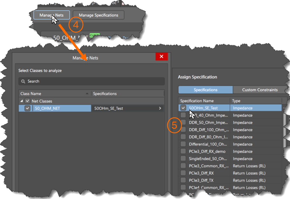
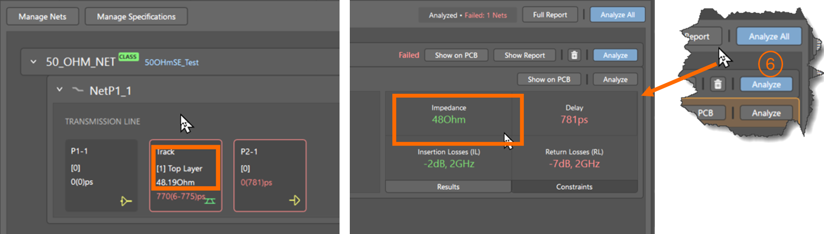
- Altium Designer에 통합된
추가 참고 사항
- 삽입 손실, 반사 손실 또는 지연 사양이 정의되지 않은 경우 SI Analyzer가 기본값으로 인해 실패를 보고할 수 있습니다.
- 제약 조건 관리자에서 명확하게 구분할 수 있도록 의미 있는 클래스 이름(예:
50OhmLine )을 사용합니다. - 외부 임피던스 계산기는 복잡한 스택업에 대해 더 높은 유연성을 제공할 수 있습니다.
- SI Analyzer는 Altium Designer의 Schematic 또는 PCB 레이아웃 환경에서 직접 실행할 수 있습니다.
참고 자료
- SI Analyzer by Keysight – 기능, 설정 및 라이선스 요구 사항을 포함하여 SI Analyzer by Keysight 확장 기능을 소개합니다.
- 레이어 스택 정의 – 임피던스 제어 라우팅에 필수적인 PCB 레이어 스택을 정의하고 구성하는 방법을 설명합니다.
- 신호 무결성 분석을 위한 설계 준비 – 신호 무결성 분석을 실행하기 전에 필요한 사전 요구 사항과 준비 단계를 설명합니다.
- KB: 레이어 스택에서 계산된 전송선 임피던스 검증 – Layer Stack Manager의 임피던스 결과를 검증하는 방법과 외부 계산기 결과와 차이가 발생할 수 있는 이유를 설명합니다.
 AI로 번역됨