
KB: How to Create a Simple Transmission Line Simulation Using the SI Analyzer Tool by Keysight
Solution Details
Transmission line impedance validation scenario and scope
The objective is to design a transmission line of a specific length and target impedance between two SMA connectors and verify that the impedance meets the acceptable tolerance range using SI Analyzer within Altium Designer.
Causes of impedance mismatch in PCB designs
Impedance mismatches in high-speed PCB designs are typically caused by incorrect trace widths, improper stack-up definitions, or missing constraint definitions. These issues can result in signal reflections, degradation, and reduced overall performance. Without proper validation using tools like SI Analyzer, these problems may not be identified until later in the design cycle.
Available methods to define impedance constraints
Feature Availability: The features available to you depend on which Altium solution you have – Altium Develop, an edition of Altium Agile (Agile Teams or Agile Enterprise), or Altium Designer (on active term).
Step-by-step workflow for simulation and validation
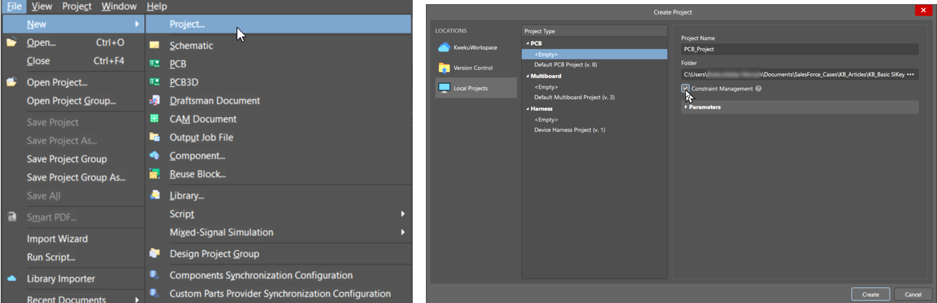
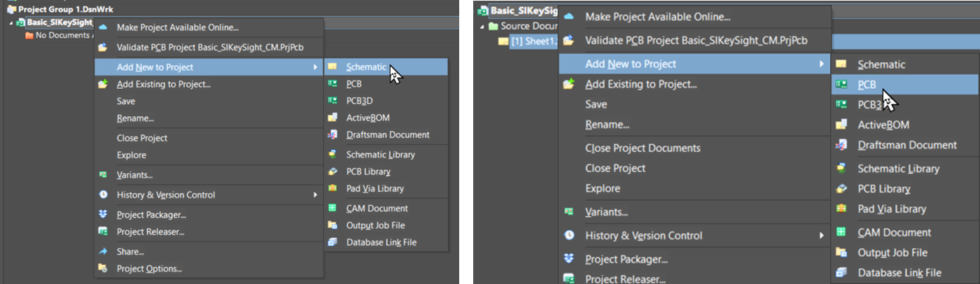
- Create the project and schematic
- Start a new project in Altium Designer.
- Add and save a schematic (
*.SchDoc) and PCB (*.PcbDoc) document. - Optionally enable constraint management during project creation.
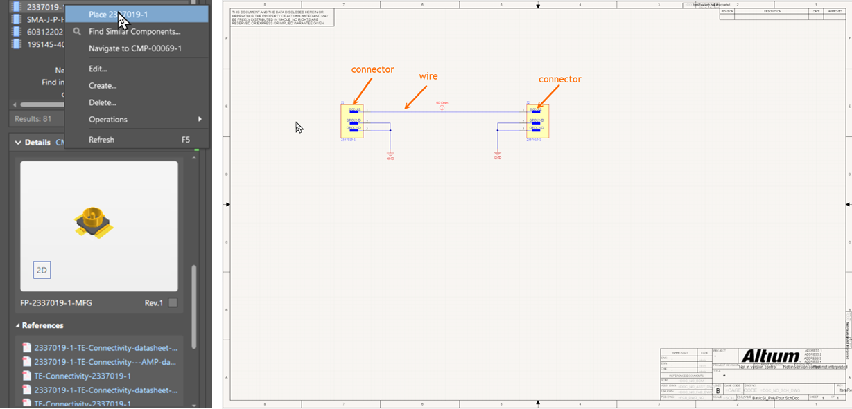
- Place SMA connectors
- Select SMA connectors from your library (local or Altium 365 Workspace).
- Place two connectors on the schematic.
- Connect signal pins with a wire.
- Connect all other pins to GND.
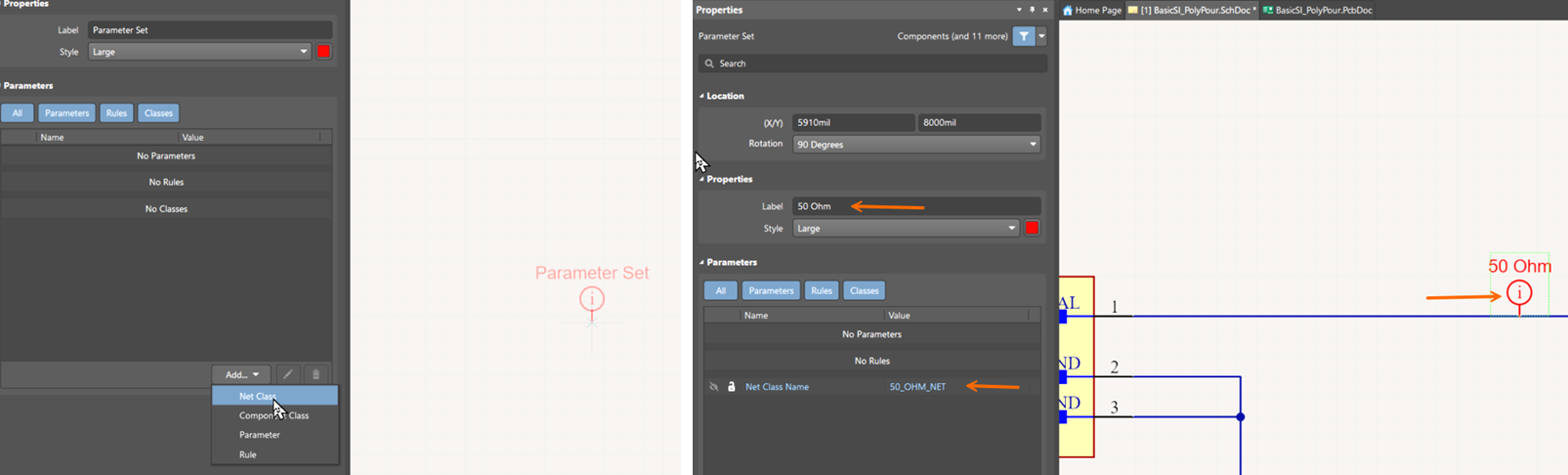
- Define impedance constraints
- Design Directives Method:
- Create a Parameter Set for the target impedance.
- Assign a Net Class Name and associate it with the signal wire.
- Constraint Manager Method:
- Open Constraint Manager from the schematic.
- Add a new class (e.g., 50OhmLine) and assign the target net.
- In the Physical tab, set the Preferred Width.
- Select the impedance profile in the Trace Width window.
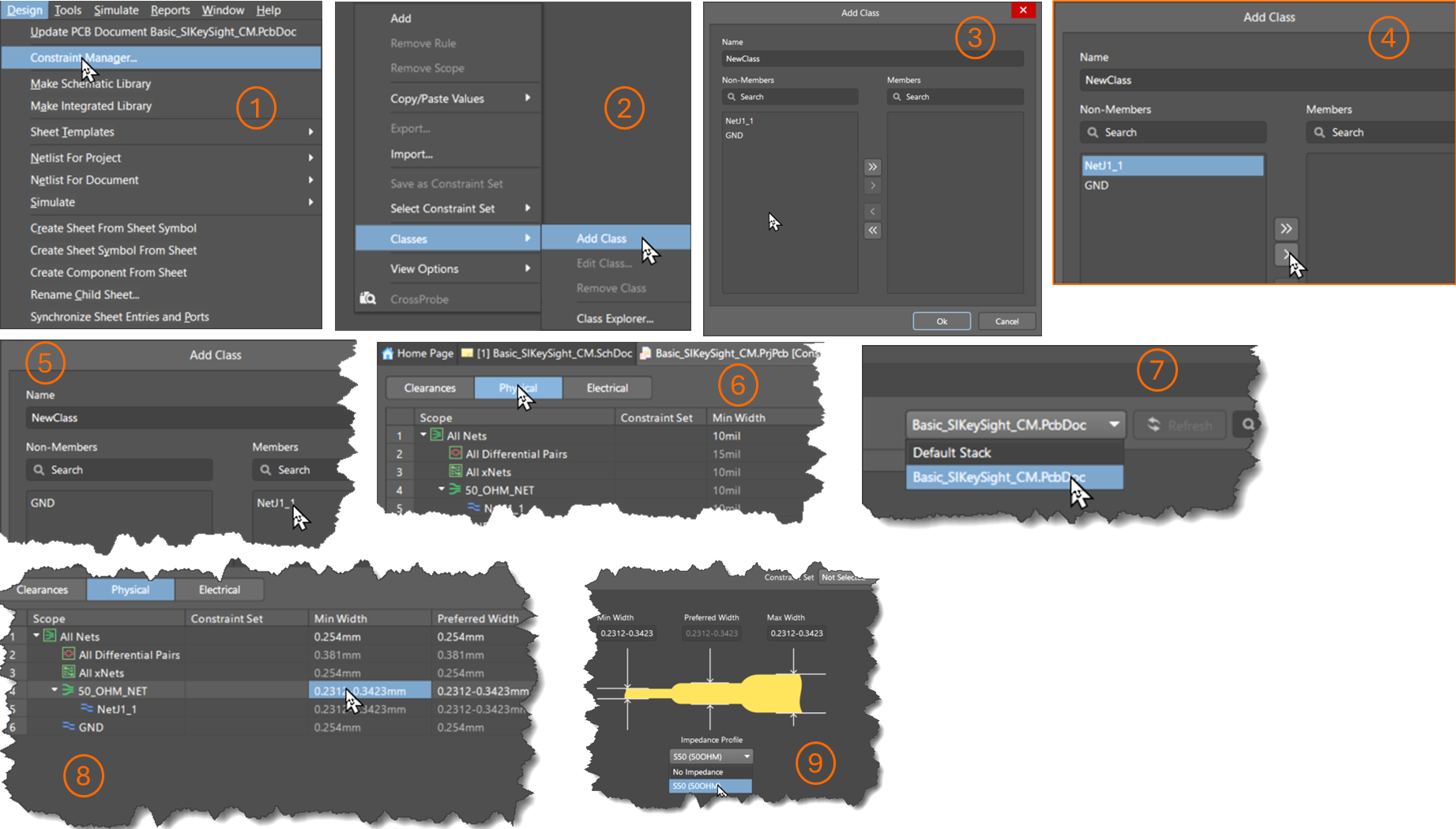
Note: The stack-up and impedance profile must be created before completing this step.
- Design Directives Method:
- Create stack-up and impedance profile
- Define the stack-up in the
*.PcbDocusing appropriate dielectric materials, thicknesses, and copper weights. - Use Altium’s impedance calculator or an external tool to determine trace width.
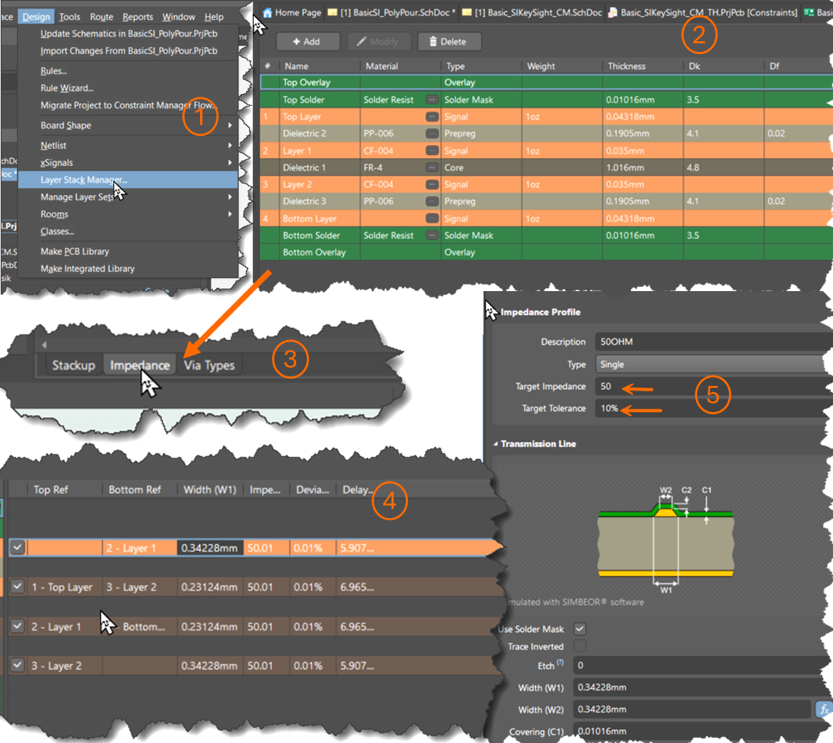
- Define the stack-up in the
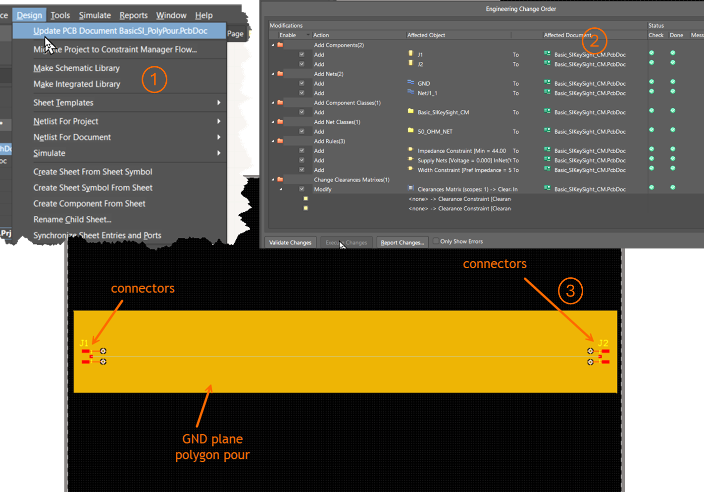
- Update PCB and complete layout
- Use Generate ECO to update the PCB.
- Place connectors on the board outline at the required spacing.
- Assign planes and polygon pours to the GND net.
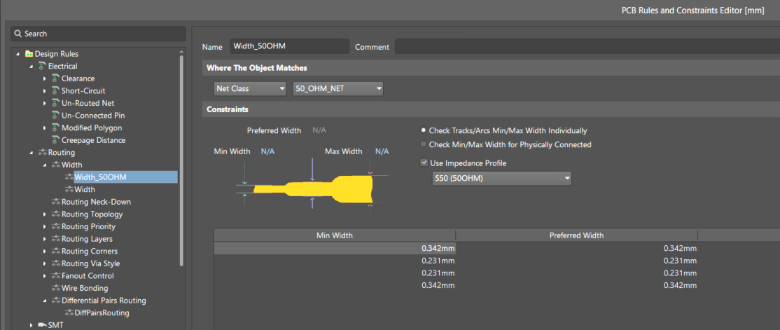
- Apply design rules and validate layout
- Create a design rule for trace width using the impedance profile or external calculations.
- Altium Designer applies impedance profiles during interactive routing via the PCB Rules and Constraints Editor or Constraint Manager.
- Connect ground pads and traces appropriately.
- Run DRC to check for errors.
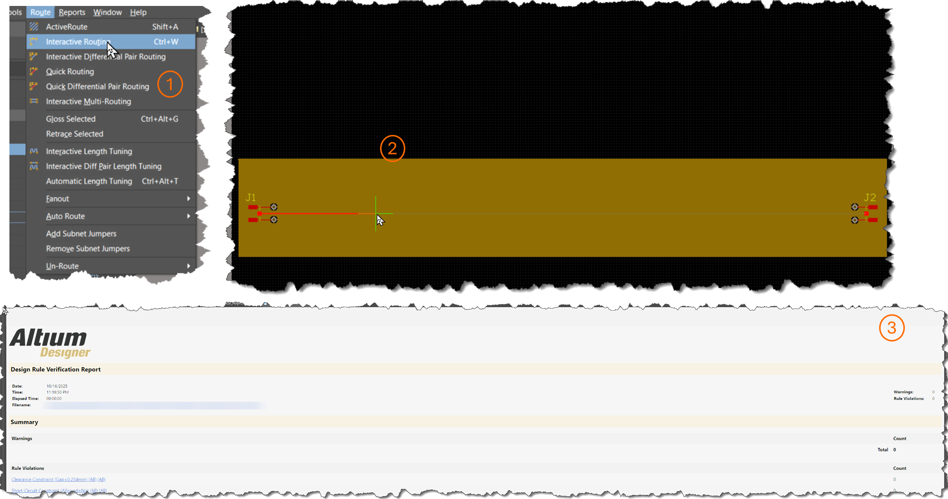
- Run SI simulation and verify results
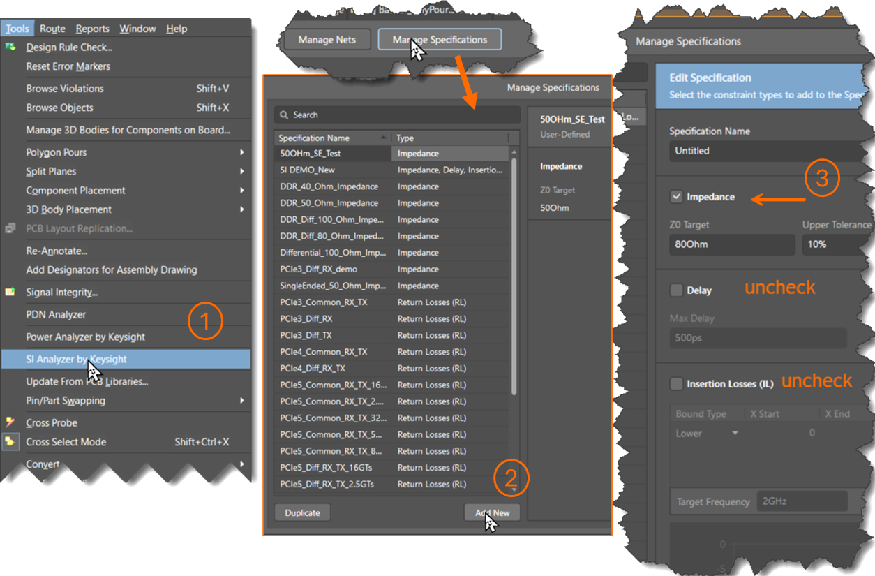
- Load the SI Analyzer by Keysight integrated into Altium Designer.
- In Manage Specifications, create an impedance specification (insertion loss, return loss, and delay may be skipped).
- In Manage Nets, assign the specification to the target net or class.
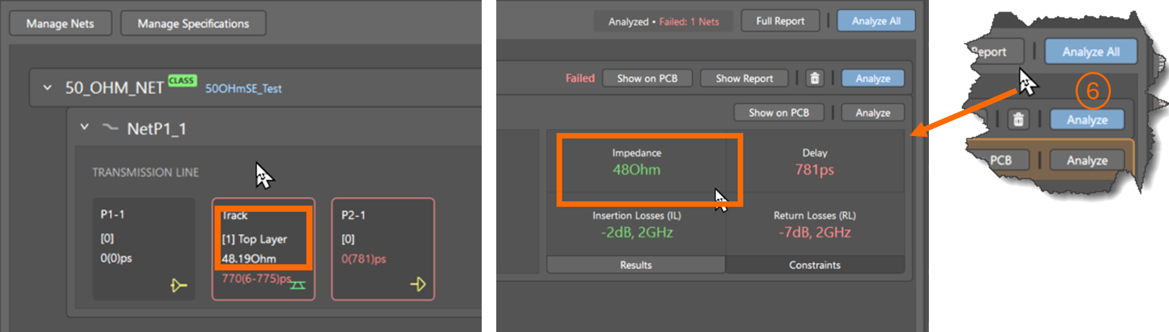
- Click Analyze.
- Confirm the impedance meets the target within tolerance.
Additional Notes
- If insertion loss, return loss, or delay specifications are not defined, the SI Analyzer may report failures due to default values.
- Use meaningful class names (e.g., 50OhmLine) for clarity in Constraint Manager.
- External impedance calculators may provide more flexibility for complex stack-ups.
- The SI Analyzer can be launched directly from the schematic or PCB layout environment in Altium Designer.
References
- SI Analyzer by Keysight – Introduces the SI Analyzer by Keysight extension, including features, setup, and licensing requirements.
- Defining the Layer Stack – Describes how to define and configure the PCB layer stack, which is critical for impedance-controlled routing.
- Preparing the Design for Signal Integrity Analysis – Outlines the prerequisites and preparation steps needed before running signal integrity analysis.
- KB: Validate transmission impedance computed in layer stack – Explains how to validate impedance results from the Layer Stack Manager and why they may differ from external calculators.