New in PDN Analyzer 1.1
The PDN Analyzer powered by CST® application for Altium Designer delivers an easy to use but powerful Power Distribution Network (PDN) analysis tool for resolving DC voltage and current density issues in board layout designs. Provided as an Altium Designer extension, it integrates power integrity analysis into the natural board design workflow.
– See PDN Analyzer and the PDN Analyzer Example Guide for more information.
The release of the PDN Analyzer version 1.1 introduces a range of new analysis functions along with bug fixes and performance refinements.
Notable new features include:
Multiple analysis through Batch Processing
An inherent part of modern digital designs is the presence of multiple power supply rails and their corresponding return paths. Performing PDN Analysis on the more complex, high density board designs can therefore involve a sequence of extended PDN simulation runs to cover all power rail networks.
PDN Analyzer v1.1 offers the ability to automate this task through a new Batch Analysis Mode, which will perform a sequence of simulation runs that can then be viewed on demand. The simulations are based on a nominated collection of predefined PDN configuration files, as saved from the PDN Analyzer panel’s main configuration screen.
To access the analyzer’s new batch mode for the currently active PCB layout, select Tools » PDN Analyzer (Batch Mode) from Altium Designer’s main menu. If the PDN Analyzer panel is already open, the command will simply add the PDN Analyzer Batch Runner tab to the panel.

The analysis batch run sequence is determined by the collection of PDN Analyzer configuration files that have been included in the displayed list. Select the  button to add configuration files (
*.pidc_config) to the list – use standard Shift-click or Ctrl-click techniques to add multiple files in one action.
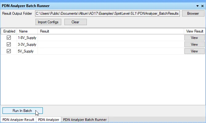
Use the  button to run the defined (and Enabled) sequence of PDN simulations, which will target their output files to the folder nominated by the Result Output Folder field. This defaults to a
 \PDNAnalyzer_BatchResults subfolder within the active project’s folder, but can be overridden by editing the field or using the  button to select an alternative location.
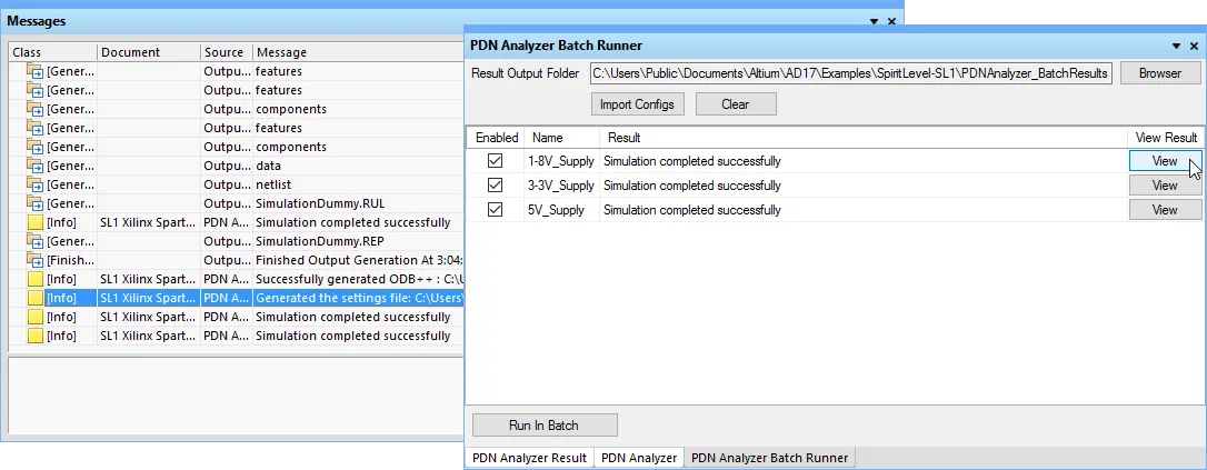
A successful sequence of PDN analyzer simulations is indicated by confirmation entries in Altium Designer’s Messages panel and the panel’s Result column (as shown above). Use an entry’s  button to display the simulation results in the PCB workspace for that PDN configuration.
The results for each PDN simulation are saved in individual subfolders named as the associated configuration, and therefore can be recalled by the PDN Analyzer as required. To view a particular simulation result (or a collection of past batch simulation results) in a subsequent session, add the configuration files again in the panel’s PDN Analyzer Batch Runner tab. Those that have been previously run will be indicated by the Simulation completed successfully entry in the Result column. Alternatively, repeating the Run In Batch command () will overwrite the existing results.
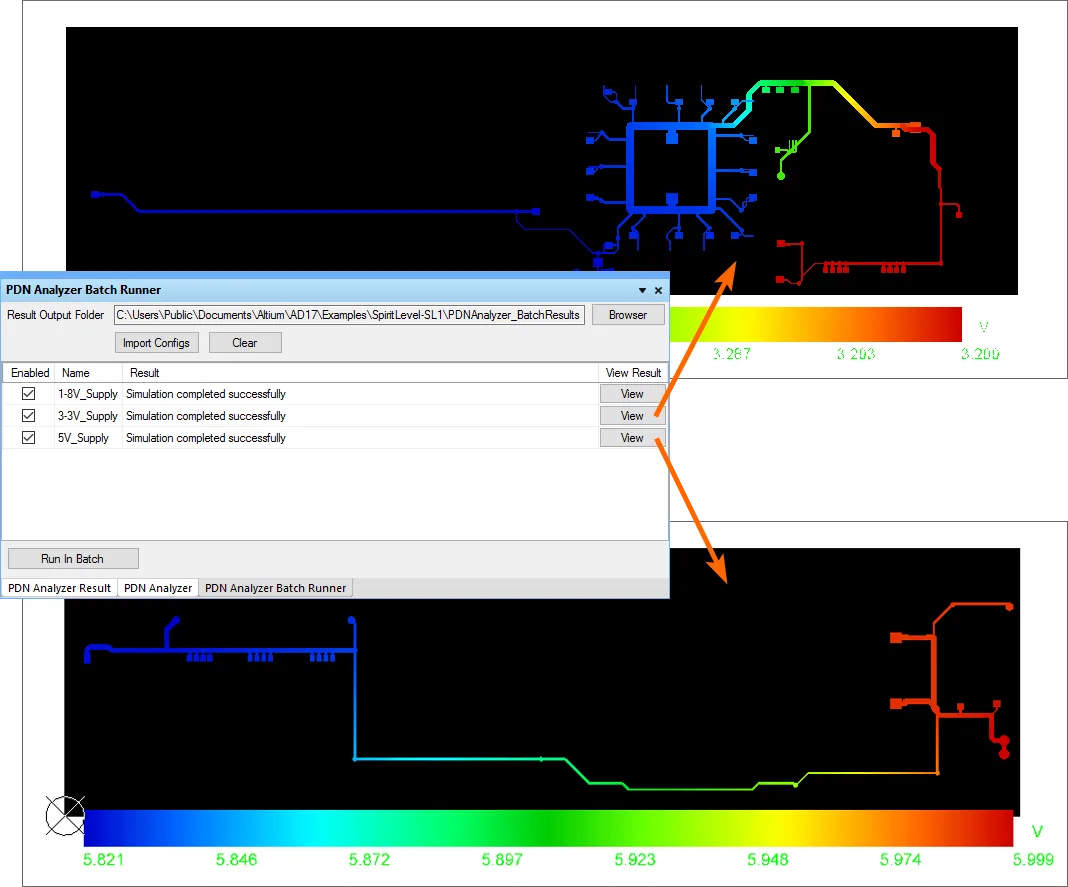
In general, at any time when the panel’s PDN Analyzer Batch Runner tab is populated with successfully run simulations (produced by either a current or past batch run), these can be displayed in the workspace by selecting the button for each entry.
In this way, the power integrity data for all supply rails in a given board design can be automatically generated, and then grouped with that project and recalled as needed. It also allows for alternative analysis permutations, such as a supply rail returned to a different ground point, to be generated and stored for comparison purposes.
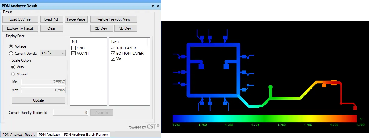
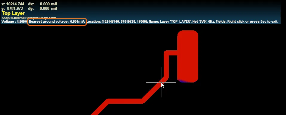
Enhanced Voltage Probing
The PDN Analyser’s voltage probe capability has been expanded to provide an additional displayed data entry that represents the voltage at the ground location nearest to the probed point.
This allows for a more accurate, relative assessment to be made of the voltage differential applied to a load at (or near) that point by taking into account IR losses in the ground path. When the probe is activated from the panel's  button and a supply rail point in the board shape is selected, Altium Designer’s Heads Up Display now includes a
 Nearest ground voltage entry along with the location point Voltage and positional data, etc.
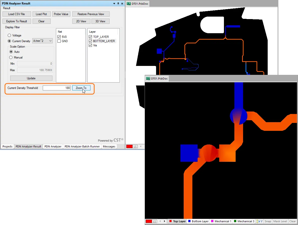
High Current Density Detection
An additional High Current Density Threshold field is now available in the panel’s PND Analyzer Result mode view. The value entered in this field acts as a defined point at which the current density level in the board shapes should not exceed, and therefore acts a current density design constraint for the board layout.
The threshold figure is relative to the Current Density units that are currently active, as determined by the drop down menu associated with the Current Density option selector. When the  button is selected, the PDN Analyzer will detect the first violation it encounters and zoom the workspace display to that point.