
TRANSLATE: KB: PCB에서 베이지색 마커 해독하기
Solution Details
DRC makers are displayed in the locations where violations have been caught upon running rule check:
Setting Up & Running a DRC
You can find more about the violations from the right-click context menu 'Violations'.
Once a violation is assumed to be resolved, and a maker still persists, it could be either that the violation is still not resolved or DRC of the particular rule has not been executed since. To verify, you can reset all makers temporarily from the top menu Tools » Reset Error Markers, and re-run the rule selectively via right-click context menu in PCB Rules And Violations panel, or in batch, from the top menu, Tools » Design Rule Check.., in the dialog click 'Run Design Rule Check..', with the particular rule enabled for batch DRC.
There are less obvious errors such as of hatched pattern on track segments, which may not appear during routing but only upon running DRC, and this could happen for a diff pair with some contention between two different rule categories, namely Gap in Differential Pair Routing rule and Electrical Clearance in Same Differential Pair .
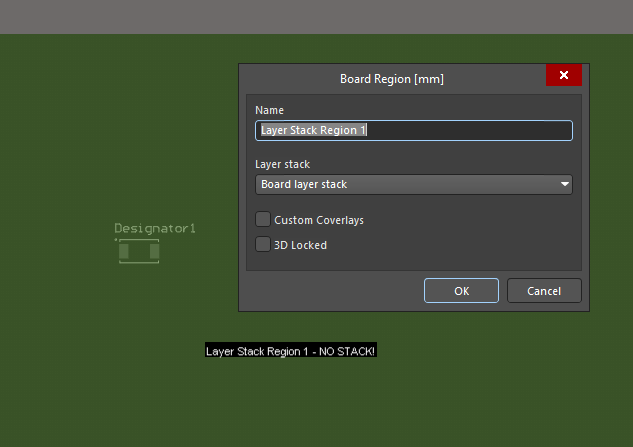
If you are observing many markers at seemingly random locations, it could be that your layer stackup definition or its assignment to board region is changed or broken somehow. As a starter, check that your stackup is defined as intended in Design » Layer Stack Manager, and then in Board Planning Mode (keyboard shortcut '1') that the board region in green has a layer stack assigned so the white text with a black box does not say 'NO STACK!'.
Rigid & Flex Regions Planning (Standard)
Assigning a Layer Stack and Editing the Board Region Name (Advanced Rigid-Flex Mode) (Advanced)