Polygon Pours can only be placed in the PCB editor. You can place them directly or create them from selected primitives.
To place a polygon pour, switch to the desired layer then place the polygon pour by choosing Home | Pour | Polygon Pour.

After launching the command, the cursor will change to a cross-hair and you will enter placement mode. Placement is made by performing the following sequence of actions:
- Position the cursor then click to anchor the starting vertex for the polygon.
- Move the cursor ready to place the second vertex. The default behavior is to place two edges with each click with a user-defined corner shape between them. Refer to the Placement Modes section below for more details on changing corner modes.
- Continue to move the mouse then click to place further vertices.
- After placing the final vertex, right-click or press Esc to close and complete placement of the polygon. There is no need to manually close the polygon since the software will automatically complete the shape by connecting the start point to the final point placed.
Placement Modes
- While placing a polygon, there are five available corner modes, four of which also have corner direction sub-modes. During placement:
- Press Shift+Spacebar to cycle through the five available corner modes.
- Press the Spacebar to flip the polygon.
- Press the 1 shortcut key to toggle between placing two edges per click or one edge per click. In the second mode, the dashed edge is referred to as the look-ahead segment (as shown in the last image in the set below).
- Press the Backspace key to remove the last vertex.


Changing Polygon Pour Shape and Location
Click once on a polygon pour object to select it, which puts it into edit mode. The outer shape of the polygon object is defined by a series of edges: where each edge is represented by an end vertex at each end, shown as a solid white square; and a center vertex in the middle, shown as a hollow white square. Each end vertex represents the location where two edges meet.
 A selected Polygon Pour
- Click and drag A to move the applicable end vertex.
- Click and drag B to move the applicable center vertex, effectively creating a new end vertex and splitting the original edge into two.
- Click anywhere along an edge, away from editing handles, and drag to slide that edge.
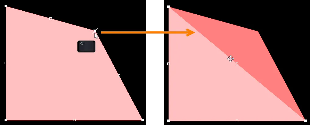
- Ctrl+click anywhere along an edge, away from editing handles, to insert a new end vertex.
- To remove an end vertex, click and hold on the vertex, then press the Delete key.
- Click anywhere on the polygon away from editing handles and drag to reposition it. While dragging, the polygon can be rotated or mirrored:
- Press the Spacebar to rotate the polygon counterclockwise or Shift+Spacebar for clockwise rotation. The Rotation Step size is defined on the PCB Editor – General page of System Preferences.
- Press the X or Y keys to mirror the polygon along the X-axis or Y-axis respectively.
If the polygon pour is currently unpoured, editing will not prompt to rebuild/unpour it. If the polygon is currently poured and you have changed its shape or location, a dialog will open asking whether you wish to repour the polygon pour now or whether you'd like to make it unpoured. Click the applicable button as required.
Multiple polygon pours can be moved simultaneously. Shift+click on all pours that you want to include in the move then click and drag on one pour in the selection to move the entire selection.
To repour a currently unpoured polygon pour after editing, right-click over the pour then use one of the Rebuild commands (or the Set All To Poured or Set Selected To Poured commands) on the Polygon Actions sub-menu (as applicable).
Define from Selected Objects
As well as interactively placing a polygon, it can also be created from a set of existing track and arc objects that define a closed shape. To define a polygon from an existing closed shape, select all primitives that form the closed shape then click Home | Pour | Polygon Pour » Define from Select Objects from the main menus.
The polygon will be created with its Fill Mode set to Outline and the Is Poured option disabled in the Inspector panel, and therefore, it will be an empty polygon. Note also that the originally selected primitives are not removed, and therefore, the new polygon will not be visible since its outline lies along the centerline of the selected objects. The selected objects can now be deleted or moved to another layer (via the Inspector panel) to reveal the new polygon. Another approach is to select the objects to be used, switch to a different layer, then run the Define From Selected Objects command to create the polygon on that layer. Enable Single Layer mode (Shift+S) and you will see the outline of the new polygon. Double-click to repour the new polygon as solid or hatched then enable the Is Poured option in the Inspector panel.
Since the Define from Selected Objects algorithm uses the centerline of the selected objects, it requires that the start and end locations of touching objects are exactly co-incident (at the same location). If this is not the case, a Confirm dialog will open and give the location where the algorithm failed, and also providing the opportunity to instruct the algorithm to attempt to define the polygon from the edges of the objects instead. As long as the selected objects overlap slightly, this option should create a polygon, with the edge of the polygon tracing the outer edge of the selected objects.
Graphical Editing
This method of editing allows you to select a placed polygon pour object directly in the design space and change its size, shape, or location graphically.
To select or edit a polygon, first switch to the layer on which the polygon is located.
An object that has its Locked property enabled cannot be selected or graphically edited. Double-click on the locked object directly then disable the Locked property to graphically edit the object.
The following section describes the key commands available from the Polygon Pour drop-down menu to graphically modify a polygon.

Move Polygon Vertices
Polygons contain two points or "handles" with which to edit the shape of the polygon.
- Full Handles - these filled handles are located at the corners of the polygon.
- Empty Handles - these blank handles are located in the centers of the segments created by the Full Handles.
An existing polygon can be reshaped by moving these handles, or vertices, located at each corner or at the center of each edge.
To modify the polygon shape:
- Click and select a polygon, which will highlight the vertices for the polygon and change the cursor to a crosshair.
- Click, hold and drag a Full Handle to move that corner.
- Click, hold and drag along an edge to move the entire edge.
- Click, hold and drag an Empty Handle to move the whole side (for track and for arc).
- Ctrl+Click on an Empty Handle to break that edge into two edges. Ctrl only needs to be held at the beginning of the movement. The Shift+Spacebar hotkeys can then be used to cycle through modes (arc, miter, and any angle). The top images show empty handle editing. In the bottom images, Ctrl has been clicked while grabbing the handle to move for editing.

- If the angle placement mode creates unwanted vertices, click and hold on the vertex and drag the edge to reduce the vertices on that edge to one. To delete a vertex, click and hold on the vertex as if you were going to move it then press the Delete key.
- When you have finished, right-click then select Polygon Actions » Repour Selected to repour the polygon in its new shape.
Polygon Pour Cutout
To create a cutout or hole inside a polygon, place a polygon pour cutout on top of the existing polygon. To do this:
- Click Home | Pour | Polygon Pour » Polygon Pour Cutout from the main menus.
- The cursor will change to a crosshair, starting inside the boundary of the polygon. Click the Left Mouse button to define the starting location.
- Move the cursor across the polygon. The cutout is actually a Region object with the Polygon Cutout option enabled. Press Shift+Spacebar to cycle through the region corner modes.
- Continue to click and move the mouse to define the cutout outline.
- Right-click to exit polygon cutout placement mode.
- The original polygon must now be repoured. Select the polygon, then use the right-click context menu Polygon Actions » Repour Selected command from the main menus - it will pour around the new cutout.
 and unpoured (right).") An example polygon pour cutout within a polygon pour that is poured (left) and unpoured (right).
An example polygon pour cutout within a polygon pour that is poured (left) and unpoured (right).
The cutout exists as an independent object; it can be moved, resized, or deleted if required. Remember that the polygon must be repoured whenever the cutout is changed.
Non-Graphical Editing
This method of editing uses the Inspector panel to modify the properties of a polygon pour object.

The Inspector panel can be accessed during placement by pressing the Tab key.
After placement, the Inspector panel is accessed in one of the following ways:
- Double-click on the placed polygon pour object.
- Place the cursor over the polygon pour object, right-click then choose Properties from the context menu.
Quickly change the units of measurement currently used in the Inspector panel between metric (mm) and imperial (mil) using the Ctrl+Q shortcut. This affects the specified measurements in the panel and does not change the actual measurement unit employed for the board as determined by the Metric and Imperial buttons in the Home | Grids and Units area of the main menus.
Polygon Fill Modes
The polygon pour placement engine can construct polygons from either solid regions or from a combination of tracks and arcs. To help you decide which of these to use, consider the following:
- Region-based polygons result in far fewer objects being placed, making for smaller files; faster redraws, file opening, DRC, and net connectivity analysis, as well as smaller output files since the region object is fully supported in Gerber and ODB++ files.
- Track/Arc-based polygons allow a hatched polygon to be created by setting the Track Width to be smaller than the Grid Size. Note that they also can be solid by setting the Track Width to be larger than the Grid Size.
- Outline Only polygons are Track/Arc polygons without the internal tracks and arcs.

 The same Polygon poured using regions, then poured using tracks/arcs.
Additional Polygon Editing Features
Poured Versus Unpoured
Polygons have an unpoured state. When a polygon is in the unpoured state, it is represented by a thin line that defines its boundary, as shown in the image below.
 The same polygon shown poured on the left and unpoured on the right.
In the unpoured state, the outline is not an electrical object, that is, it will not cause rule violations, such as a clearance or short circuit violation; the outline is displayed so that you are aware that the polygon exists and you can edit and manipulate the polygon as required.
An unpoured polygon can be:
- Reshaped.
- Moved to a new location.
- Repoured via the right-click menu or the Home | Pour | Polygon Pour submenu.
- Unpoured again via the right-click menu.
Use the Home | Pour | Polygon Pour submenu to repour All, Selected, or Violating Polygons.
Rebuilding Polygons
If you have changed the design within a polygon, it will need to be repoured to clear any violations created by the design changes. Since a polygon pour can exist in poured and unpoured states, the term 'Repour' becomes slightly inadequate. To better describe the process of reanalyzing and recalculating a polygon, the more appropriate term 'Rebuild' is employed. To rebuild polygons, right-click over a polygon in the design space then use the appropriate Rebuild command from the Polygon Actions sub-menu.
Exploding a Polygon Pour
A polygon pour can be converted to its set of primitive objects by using the Explode Selected Polygons To Free Primitives command (for one or more currently selected polygons) from the Polygon Actions submenu. Solid polygons will revert to region primitives, while hatched polygons will revert to tracks and arcs. Once exploded, a polygon pour object can no longer be manipulated as a group object.

 AI 翻译
AI 翻译