KB:控制连接同一网络对象的线条外观
Solution Details
Connection lines appearance is controlled in more than a few ways.
There is a master switch to turn on/off the display of all connection lines from the menu choice of the PCB editor:
- View » Connections » Show All (or Hide All)
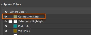
There is another switch in the View Configuration panel:
- View Configuration (panel) » Layers & Colors (tab) » System Colors (section) » turn eyeball (visibility icon) on/off for Connection lines
You can control connection lines on an individual net basis from the PCB panel:
- Select Nets view from the drop-down, then select <All Nets>. In the Nets section, double-click on a net to open the Edit Net dialog where you can verify the status of the "Hide Connections" checkbox.
- To change color, select the ones from the list below for which you want to change the color, then right-click on the selected Net(s) and choose Change Net Color, select the color you want, and click OK
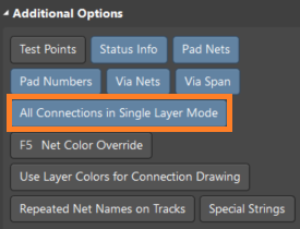
To affect Single Layer Mode (Shift+S), check this:
- View Configuration (panel) » View Options (tab) » Additional Options (section) » button for "All Connections in Single Layer Mode" on/off
If you observe connection lines not terminating to objects as expected, try:
- Design » Netlist » Clean All Nets
If you've tried everything above, and your connections lines still are not visible there is one other thing to check. Open your PCB Panel and verify that the pulldown option at the top of this panel is *not* set to From-to editor. If the PCB Panel is in this mode, it can only display connection lines for the from-to you are viewing or editing.
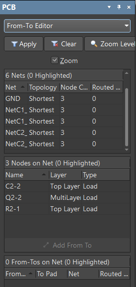
Set this pulldown to any other option, such as Nets and your connection lines should again be visible. Here's documentation with more information on the From-To editor:
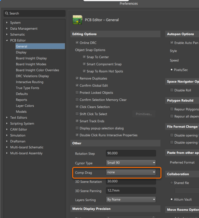
During the move component command, the behavior may vary between the menu Edit » Move » Component and mouse operation of clicking and dragging the footprint. To have the connection lines move with the component when using Edit » Move » Component, as they do when just clicking and dragging the component in the PCB editor, "Comp Drag" must be set to "None". See Preferences » PCB Editor » General » Other (section) » Comp Drag set to "None". Either way, they will show on the component when you are done.
If tracks have been placed, then for the:
None setting: Connection lines will be shown while dragging but the tracks will not move.
Connected Tracks setting: Tracks will move with the component.
-Hidden (No connection lines)
-Pad to Pad connect
-Break (Route to Route)
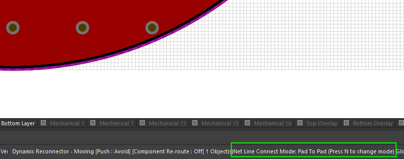
While dragging the component, cycle through the connections by pressing N. You can view the current mode in the HUD:
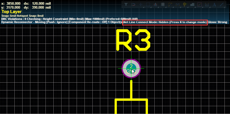
Or in the Status Bar at the bottom:
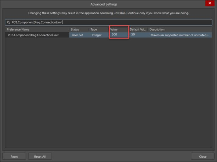
If the component has a large number of connections (i.e. more than 50 connection by default), check Preferences (gear icon in the top right) » System » General » Advanced button » Search for PCB.ComponentDrag.ConnectionLimit » Increase the value to 500. Increasing the number to 500 means components with 500 connections or less will show. If the component has more than 500 connections the number should be increased accordingly.