Working in harmony with component placement, routing is a key factor in the success of your PCB design. Altium Designer includes a number of intuitive interactive routing features to help you efficiently and accurately route your board, from a simple double-sided board, all the way through to a high density, high speed, rigid-flex, multi-layer board.
Altium Designer has a number of interactive routing capabilities, including:
-
The interactive routing tool. Interactive routing is fast and efficient, with walkaround, hug and push, and push modes that let you get the job done quickly and efficiently.
-
There is full support for differential pair routing, as well as single-sided and differential pair length tuning.
-
You also might like to explore ActiveRoute, an automated interactive routing technology that delivers efficient multi-net routing algorithms, applied to the specific nets or connections that you select. ActiveRoute also allows you to interactively define a route path or Guide, which then defines the river along which the new routes will flow.
-
The topological autorouter produces routes like that of a skilled board designer. Being a topological router, it is not constrained to an orthogonal grid, instead being guided by preferred direction settings and connection paths.
-
Nowadays, routing is no longer a simple, join the dots process. Fast device switching speeds mean that many boards have high-speed signals, requiring impedance profiles to be defined, and controlled impedance routing. The PCB editor's routing width design rule can be width-driven or it can be impedance-driven, where the routing width changes as the routing moves from one layer to another.
Is it Ready to Route?
There is a saying that PCB design is 90% placement and 10% routing. While you could argue about the percentages, it is generally accepted that good component placement is the most important aspect of good board design – determining the flow of the connections between the components. Like the routing, component placement is fluid and can be updated throughout the design process, as needed.
Still not sure if you are ready to jump into routing? use the following as a quick checklist...
Configure the Layers
A printed circuit board is fabricated as a set of discrete layers: copper layers, mask layers, component overlays, solder resist layers, along with a variety of other special purpose layers, all become part of the final fabricated PCB. Configure the layers your board will need before you start routing.
Configure the Layers
|
| Configure the copper layers |
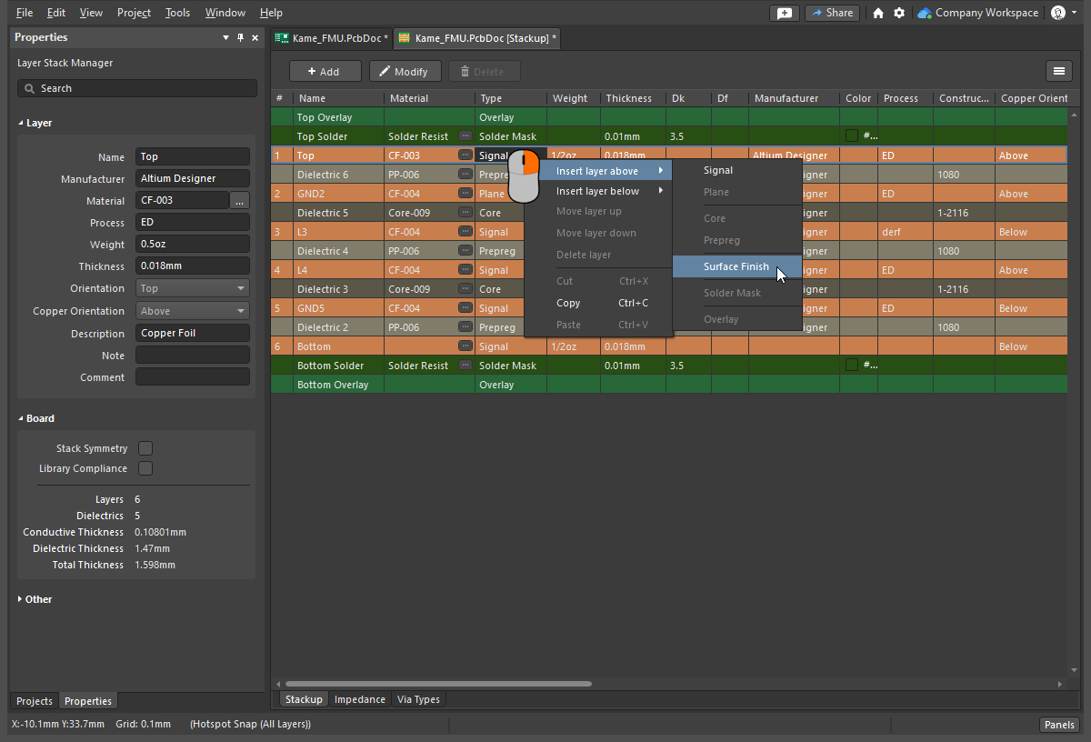
Routing layers, also referred to as signal layers, are set up in the Layer Stack Manager, as shown above. Use the main menu commands to select a pre-defined layer stack, then right-click to add layers and set their location in the layer stack.
Learn more about configuring the layer stack.
|
| Other fabrication layers |
Power planes, soldermasks, component overlays – all of the other layers that are part of fabricating the printed circuit board, are also set up in the Layer Stack Manager. |
| Add Mechanical layers |
Mechanical layers can be used in pairs, for side-of-board related tasks such as component courtyards, or individually, for general-purpose tasks such as the board outline. Mechanical layers are added in the View Configuration panel (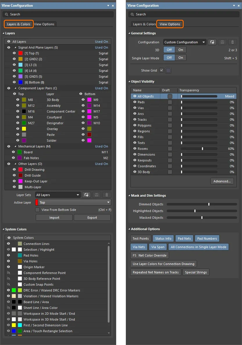 ). ).
Learn more about mechanical layers.
|
| Controlling the display of layers |
The visibility of all layers is configured in the View Configuration panel (), press L at any time to open the panel. As well as toggling layers on and off, you can also control the transparency, the dim level of faded objects, and the display of design detail such as the net names.
Learn more about configuring the display of layers in the View Configuration panel.
|
Set up the Design Constraints
The PCB editor is a constraints-driven design environment – the width of each net that you route, the size of the via that gets placed when you change routing layers, and their clearance from other objects on the board – are all controlled by the applicable design constraints. The constraints are a fundamental element of your design, and a well configured set of constraints will contribute to how quickly and effectively you can route the board.
 The Constraint Manager is a document-based, spreadsheet-like user interface that allows you to view, create, and manage the design constraints used for your PCB designs.
Are the Design Constraints Ready
|
| Am I using Design Rules or the Constraint Manager? |
The original interface to the PCB editor's rules engine is a dialog, the PCB Rules and Constraints Editor (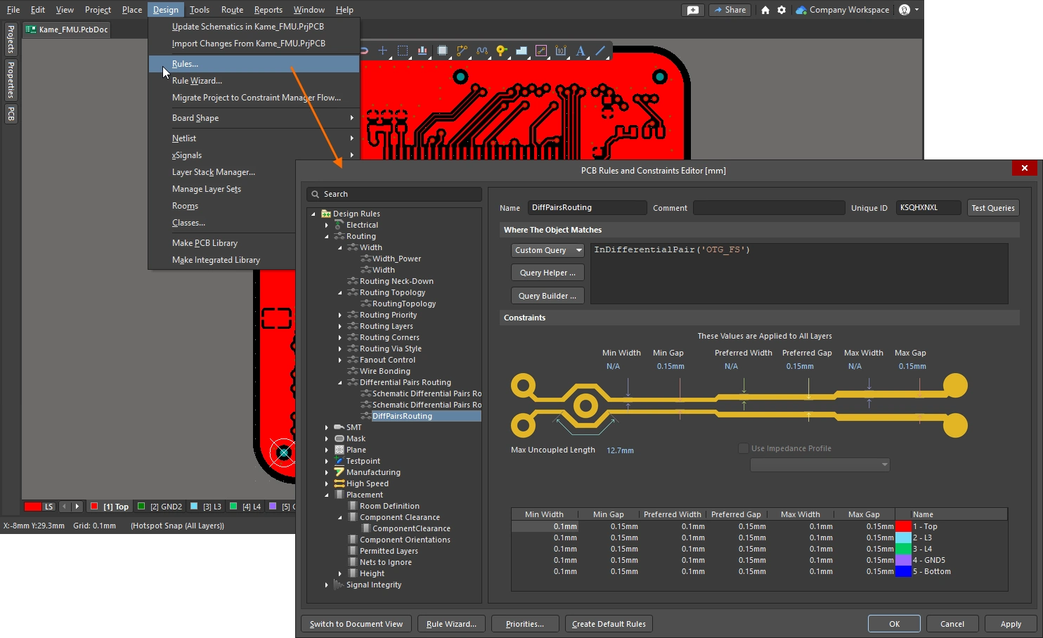 ). While this is an excellent interface for configuring the design requirements, it does not incorporate support for rule-related features such as the configuration and management of design classes. Nor does it support the definition of design constraints early in the development cycle, during schematic capture. ). While this is an excellent interface for configuring the design requirements, it does not incorporate support for rule-related features such as the configuration and management of design classes. Nor does it support the definition of design constraints early in the development cycle, during schematic capture.
The introduction of the Constraint Manager (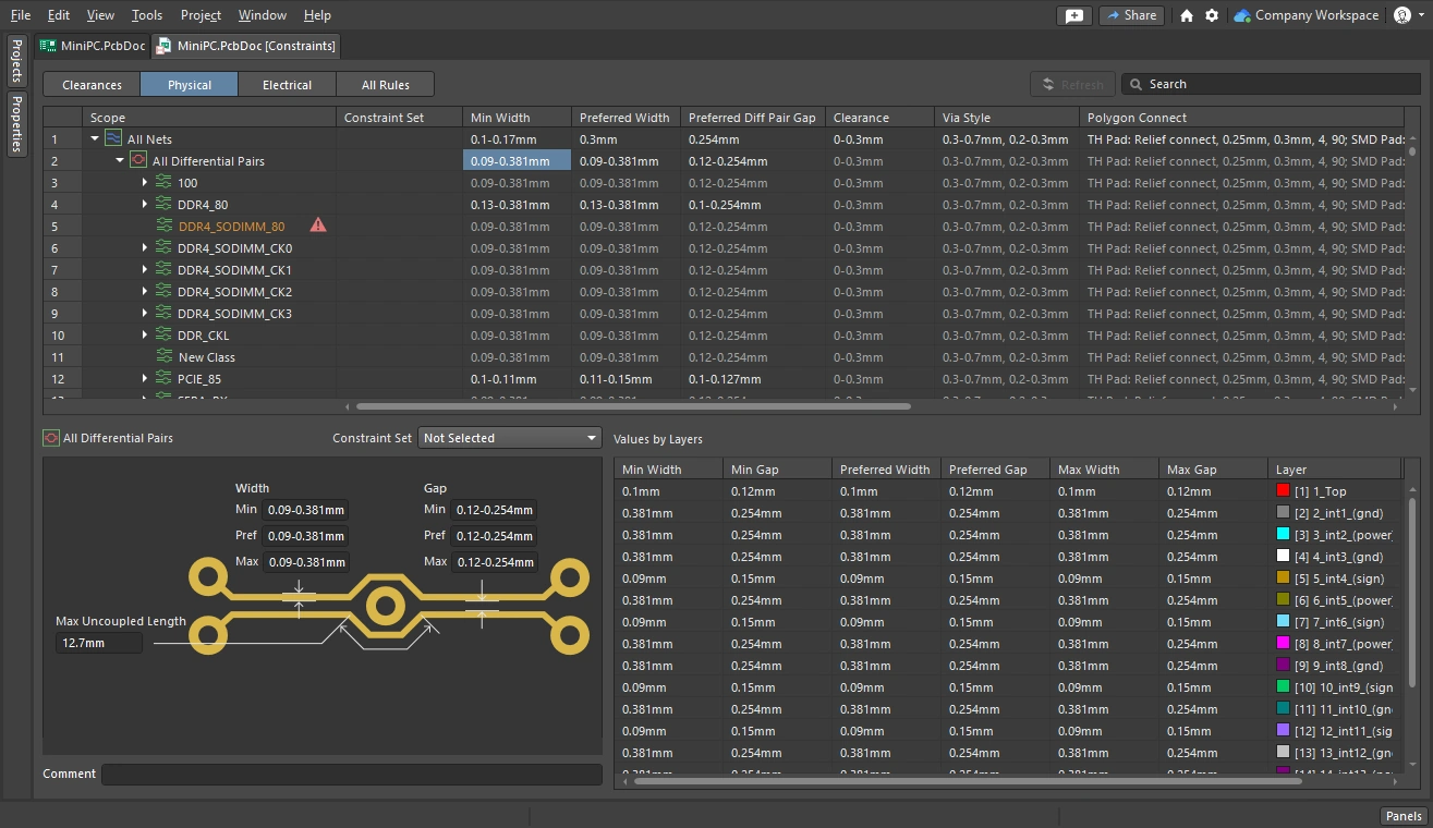 ) brings a simpler and more structured approach to defining requirements such as classes, along with the other physical and electrical requirements of the design. Constraints become project-level settings that can be edited at any time from either the schematic editor or the PCB editor, but must still be synchronized through the ECO system. ) brings a simpler and more structured approach to defining requirements such as classes, along with the other physical and electrical requirements of the design. Constraints become project-level settings that can be edited at any time from either the schematic editor or the PCB editor, but must still be synchronized through the ECO system.
To check which design constraints approach is used in your current PCB project, see if the Design » Constraint Manager command is available in the main menus of the Schematic editor or PCB editor when a schematic or PCB document is open. If the command is there, then the Constraint Manager is used for this project. Otherwise, if you see the Design » Rules command in the PCB editor, then the PCB Rule and Constraints Editor dialog is used for this project. You choose which approach is used when the project is first created. Learn more about the Constraint Manager.
|
| What is a design rule, or design constraint |
Rather than requiring you to define the attributes of every routing object that you place, the PCB editor uses a constraints system (also called the rules engine), to define the properties of the objects placed during interactive routing. For example, when you place a track on the GND net the PCB editor asks the rules engine what constraints apply to, and between, this object and its neighbors - the rules engine returns the requirements, for example this net must be 0.3 mm wide, and must be kept 0.2 mm away from any copper in other nets.
There are two key aspects to a design rule/constraint - what settings it must have (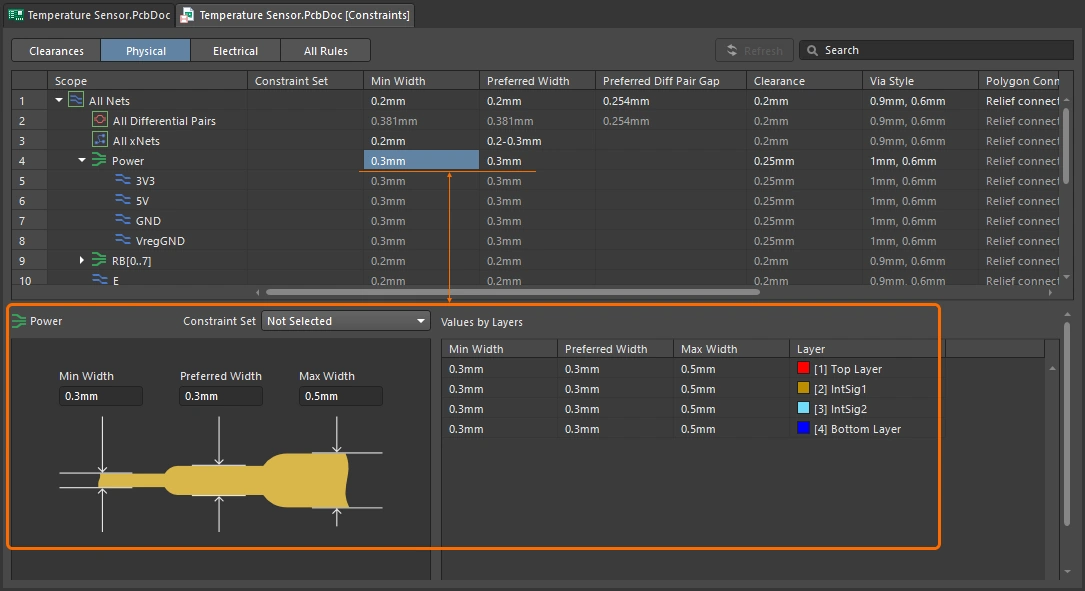 ), and what objects it applies to (the scope) ( ), and what objects it applies to (the scope) (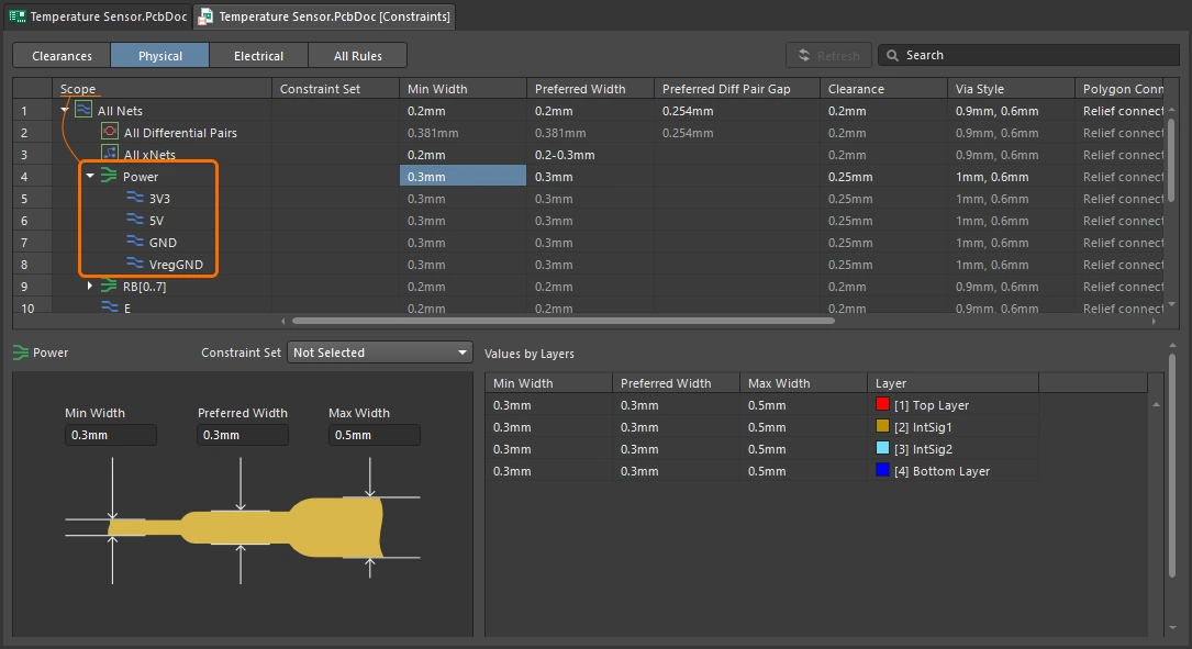 ). ).
|
| The constraint (settings) |
This is the settings you want applied to the object – it could be the width of the route, the size of the via, or the clearance between copper objects (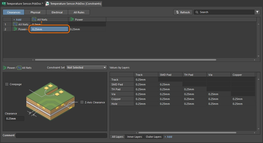 ). ). |
| The scope |
The scope defines the set of objects that this design constraint applies to (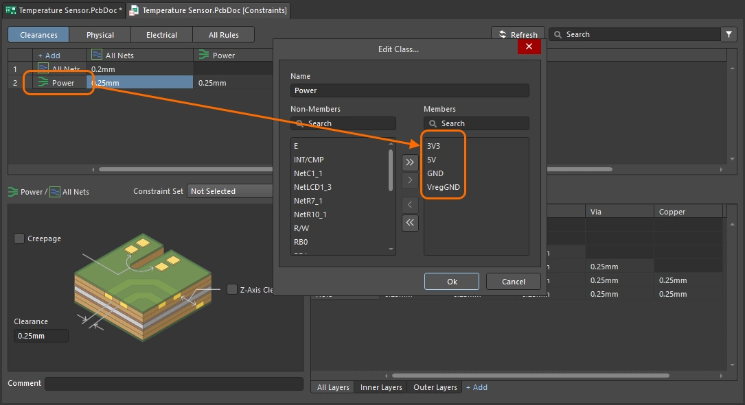 ). It could be all objects on the board, or in this component class, or that differential pair. Rules have a priority, so the constraint that defines the routing width of all nets is overridden by a higher-priority constraint that targets the power nets. ). It could be all objects on the board, or in this component class, or that differential pair. Rules have a priority, so the constraint that defines the routing width of all nets is overridden by a higher-priority constraint that targets the power nets. |
| The width constraint |
The Width constraint defines the minimum, preferred and maximum widths of the track segments that make up the routing. The settings can be defined as physical widths, or require the net(s) to be routed using a specified impedance profile. A handy feature is the ability to change the routing width between the minimum and maximum settings as you route, or have the route automatically narrow to fit through a tight location. You can read more about these features in the Interactive Routing page.
Learn more about the routing width constraint.
|
| The clearance constraint |
Working with the width constraint is the clearance constraint, it defines how close the net you are routing is allowed to get to other objects on the board. Again, you can define multiple clearance constraints, to keep higher voltage nets or differential pair nets away from other routing, or to keep polygon pours a specific distance from routing, and so on.
Learn more about the clearance constraint.
|
| The routing via style |
The third core constraint to configure before you start is the routing via style. This constraint defines the via that is automatically placed as you switch layers during routing. Like you can with the routing width, as you route you can change the via size between the minimum and maximum settings, or change the via style (the layers it spans), more on these shortcuts in the Interactive Routing page.
Learn more about the routing via constraint.
|
You have configured the clearance, routing width and routing via style design constraints – you are now ready to route! When you click to start routing, how does the router know what track width to use, and what via size to use when you switch layers? You can find a summary of how you control these properties, along with a demonstration video on the Interactive Routing page.
Finding the Nets
A good approach to routing is to work from the schematic, where you can easily locate important components and critical nets. You can cross-select and cross-probe directly from the schematic components and nets, highlighting the equivalent items on the PCB. Learn more about cross-selection and cross-probing between the schematic and the PCB editor.
You can also control the display of the connection lines by masking or hiding the nets you are not interested in. Another approach is to set the color of important nets to help you manage the routing process, there is a summary of these features below. Learn more about Managing the Display of the Connection Lines.
An unrouted board can appear intimidating – a mass of connection lines crisscrossing the board. For obvious reasons, this mass of connection lines is often referred to as the ratsnest. If you're interested in a deep-dive into the ratsnest and the connectivity it represents, check out the Understanding the Connectivity page.
Adding Color to the Nets
|
| Applying color to nets |
In the PCB editor, all connection lines have a default color applied, and then once they are routed every net displays in the color of the layer that they are routed on (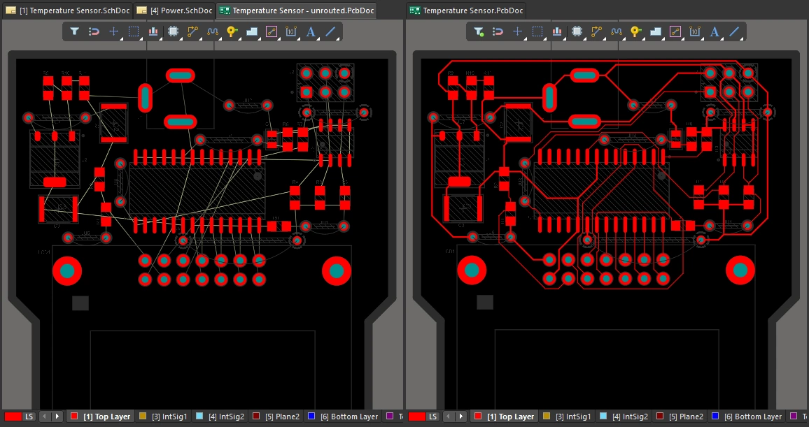 ). To make it easier to interpret the design you can change the color of the connection lines, and configure the PCB editor to use that color on the routing, using a feature called net color override ( ). To make it easier to interpret the design you can change the color of the connection lines, and configure the PCB editor to use that color on the routing, using a feature called net color override (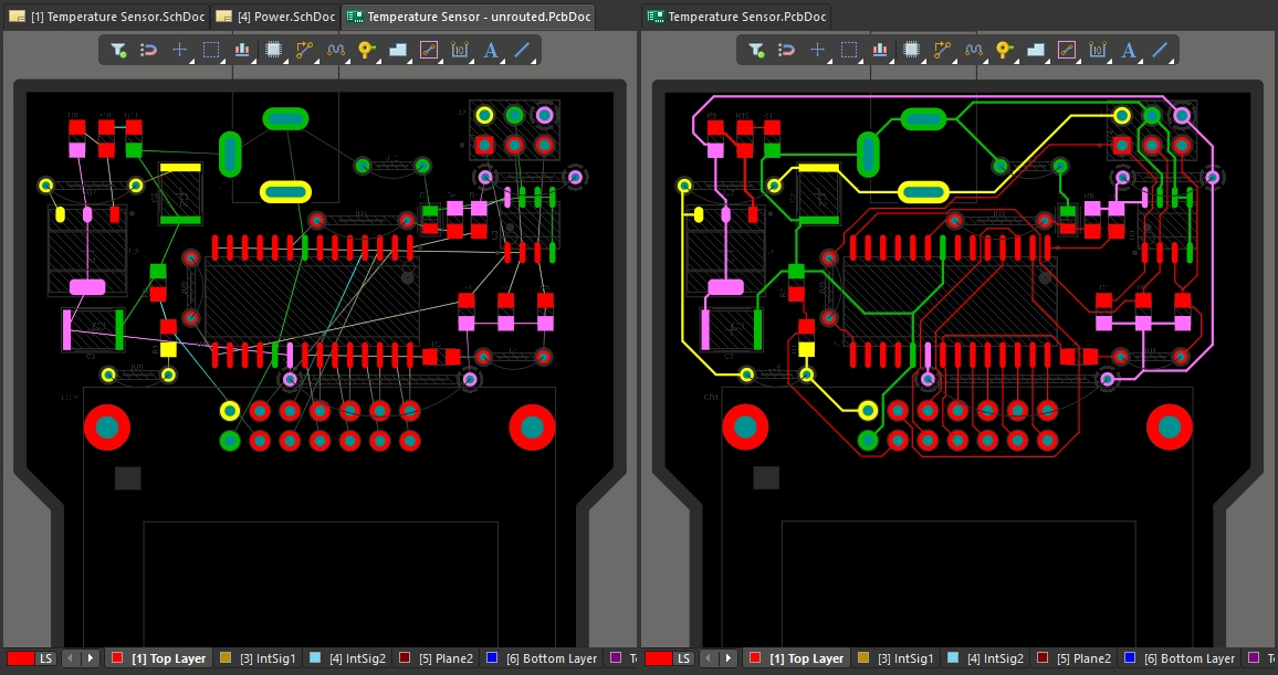 ). ).
|
| Apply the color in the schematic |
If required, you can apply color to nets in the schematic, using the View » Net Colors submenu (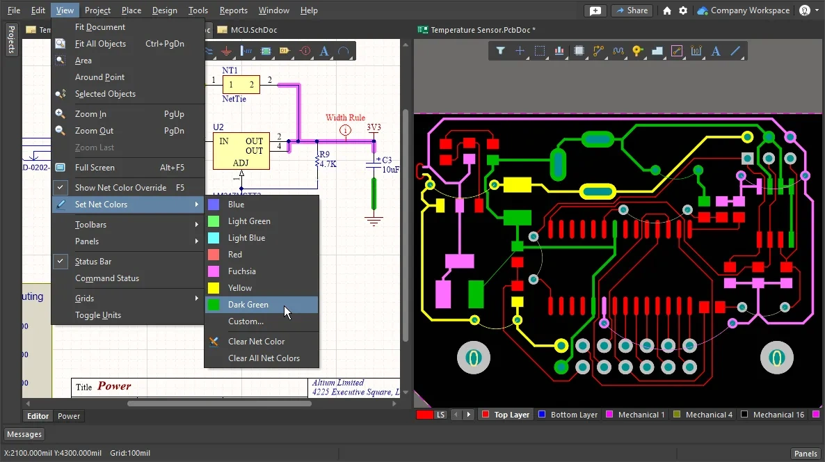 ). The colors are transferred to those nets in the PCB when the design is synchronized. ). The colors are transferred to those nets in the PCB when the design is synchronized. |
| Apply color in the PCB editor |
It is not a requirement that net colors are applied on the schematic, if you prefer the net colors can be defined directly in the PCB editor. The easiest way to do this is in the PCB panel, where you can apply changes to a single net, a class of nets, or a set of nets that you have interactively selected. Use the standard Windows selection techniques to select multiple net names in the Nets mode of the PCB panel, then right-click and select the Change Net Color command from the right-click context menu (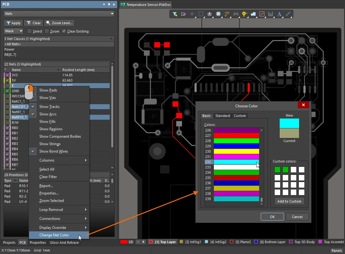 ). ). |
| Apply the color to the routing |
In the PCB editor, the net color override feature can be controlled at the individual net level, allowing you to switch it on for just the nets you are interested in right now (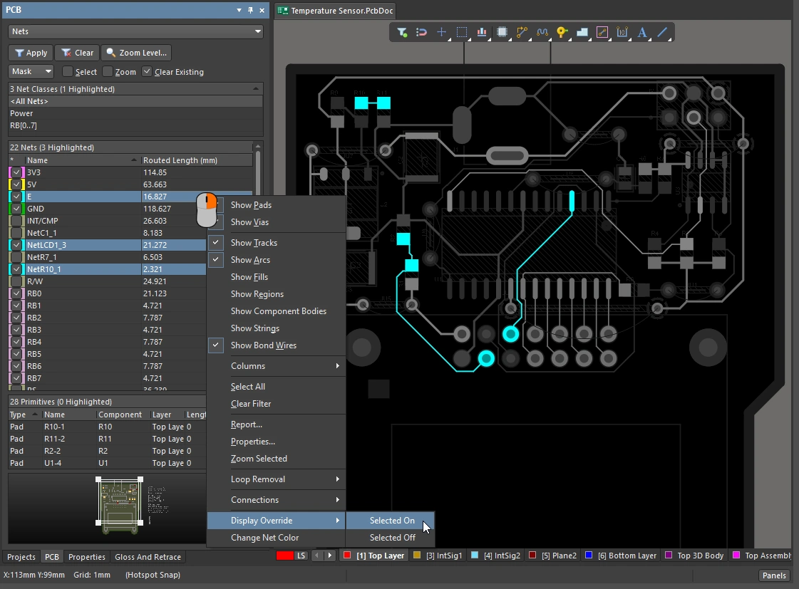 ). ). |
| Toggle the Net Color Override feature on and off |
Net color override can also be toggled on (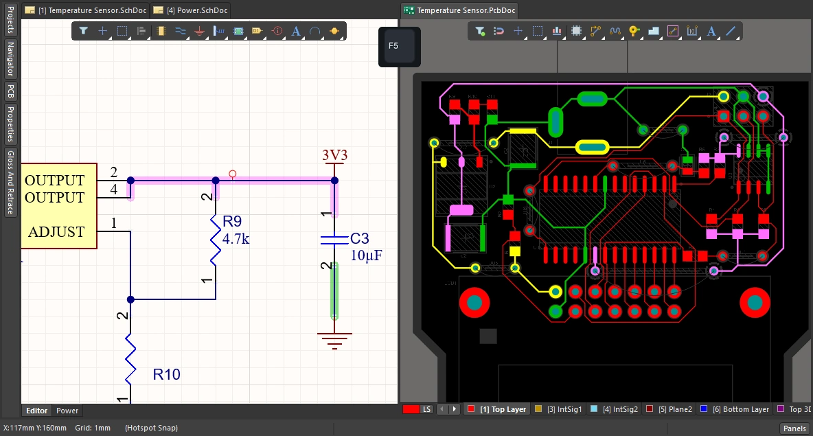 ) and off ( ) and off (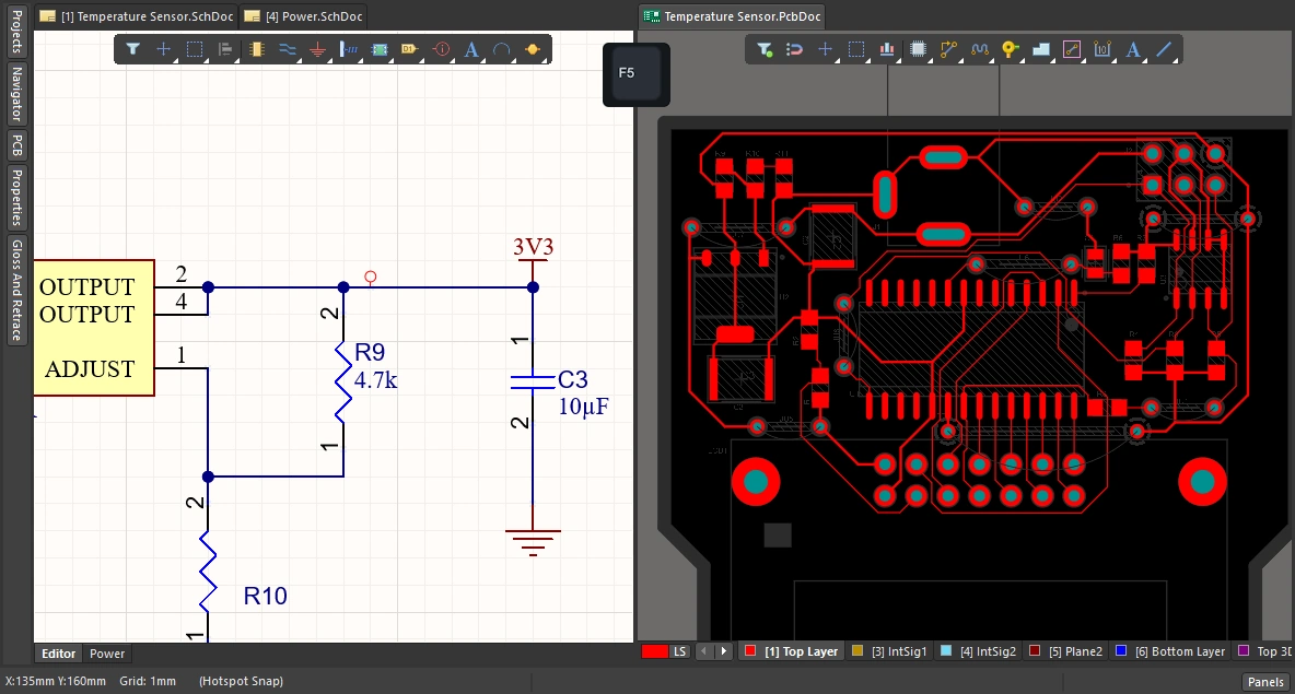 ) in both the schematic editor and the PCB editor, by pressing the ) in both the schematic editor and the PCB editor, by pressing the F5 shortcut. |
Learn more about using color to highlight nets.
