PDN Analyzer (by CST)
The PDN Analyzer powered by CST® (Computer Simulation Technology) integrates directly with Altium Designer to allow PI-DC simulation and analysis of the current PCB project. Since the PDN Analyzer functions within Altium Designer there are no manual data import/export requirements, data conversions or separate applications to be run – simply start the PDN Analyzer from the Schematic or PCB editor, set the desired test parameters and run the simulation. The results are primarily delivered through 2D/3D modeling of the circuit board copper layout, allowing a quick assessment of the results and the opportunity to perform exploratory 'what if' testing of the PCB layout design.
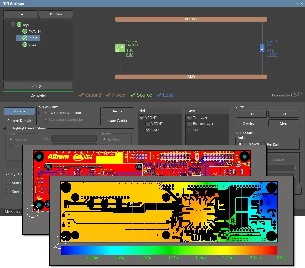
The PDN Analyzer interface shown with the Altium Designer Spirit Level example PCB, and the results of a PI-DC Voltage Drop simulation of its Top layer GND net return for the VCCINT supply.
Accessing the PDN Analyzer Functionality
To access the PDN Analyzer functionality in Altium Designer, the PDN Analyzer software extension must be installed. This extension can be installed or removed manually.
For more information about managing extensions, refer to the Extending Your Installation page (Altium Designer Develop, Altium Designer Agile, Altium Designer).
In order to access the functionality, you also need to be validly subscribed to the PDN Analyzer.
Power Integrity Essentials
In essence, the PI-DC (or 'IR drop') problem is fairly straightforward: the resistance embodied in the board's power supply shapes (traces, polygons, planes, etc.,) consumes power and voltage, robbing those from the various loads. As you would expect, the IR issues will increase in complexity with the number of loads on the supply through interaction in the power and ground copper paths.
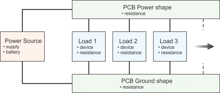
Figure 1: A basic block diagram of the power and ground shapes, and the applied loads.
Figure 1 (above) shows a simple block diagram of a circuit's power source and its power and ground shapes (traces and planes) that deliver power to the various loads (memory, microcontrollers, etc.). Note that all the loads are tied to the same power and ground shapes, and depend on those shapes to provide their operating voltage(s). In general, we tend to assume that those power and ground shapes have 0Ω resistance, which isn’t necessarily true, and that assumption can cause problems. Because relatively large currents are often involved, even small resistances in the power and ground shapes can cause significant power consumption (loss) and voltage drops.
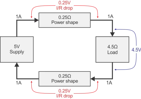
Figure 2 demonstrates an example of the problems that can arise if the resistance of the power and ground shapes are not properly considered. Even though each shape has a relatively small resistance of only 0.25Ω, they have caused the voltage at the load to drop from 5V to 4.5V. The designer has to be aware of this drop and ensure it can be accommodated, or change the design to lessen it, to ensure that that the final design will not fail in the field.
The problem, however, seems easy to solve – simply make the power and ground shapes short or large enough to represent an insignificant resistance, using the following relationship: R = ρ * L/A, where:
-
Ris the total resistance of a shape (trace or plane) -
ρis the resistivity of the material used for the shape (typically copper,ρ ≈ 1.7µΩ-cm) -
Lis the length of the shape -
Ais the cross-section area of the shape (widthxthickness)
Put simply, if you make your power and ground shapes short, thick and wide, you will minimize their resistance.
The difficulty with that, however, is that overly large shapes consume valuable routing space and may limit the amount of space for other voltage shapes. A design which has the properly sized power and ground shapes will be more compact and use fewer layers than one which arbitrarily uses overly large planes or traces. The intent of PI-DC analysis is to inform a designer that the board design's power and ground shapes are adequate, but not overly large.
Another consideration for IR drop is the fact that the amount of power consumed is I2R – so a small increase in current through a resistance causes a large increase in power consumption. This can manifest itself as thermal problems where the design heats up significantly because the power and/or ground shapes are not large enough to accommodate the current passing through them. By ensuring very small IR drop through power and ground shapes, power consumption in those shapes is minimized.
At the extreme, if a shape is resistive enough (very narrow and long) and has sufficient current flowing through it, that shape essentially becomes a 'fuse', thereby melting the copper shape and causing the design to fail – and possibly presenting a dangerous situation. The IPC-2152 standard for PCB current carrying capacity addresses this issue, but with pessimistic assumptions (no nearby thermally conductive copper to help draw heat away, for instance) and designers often apply that specification using the most conservative assumptions, such as only allowing a minimum temperature increase. While PI-DC cannot replace the IPC-2152 standard as a guideline for thermal considerations, it can give valuable insight into how a design can safely be optimized by studying the voltage drops and current densities of the power delivery system. A design that is optimized for the lowest current density and voltage drop between the sources and all loads will also generate less heat and have less chance of thermal issues.
Another aspect PI-DC analysis addresses is the number of vias used for power delivery. The problem is quite similar to that of sizing the copper shapes properly: if there are not enough vias, voltage is lost and power is wasted through IR drop, but if too many vias are used, valuable routing real estate is wasted. In particular, if too many vias are used for a particular voltage path, those vias pass through shapes on other layers and reduce their copper cross-section, thereby causing problems for those other voltages. In the same way as correctly dimensioning shapes, analyzing the voltage at the load points allows proper via sizing and/or numbering.
Finally, there is a significant advantage in simulating the final design exactly as it appears physically, to ensure it is optimized. PI-DC simulation provides a final check that connectors and regulators are sized appropriately, in case loads have been dropped or added during the design process, for example.
In the absence of reliable data on the voltage drop through a PCB's various power shapes, ground shapes and vias, a designer is forced to be conservative by using excessive plane shapes, trace sizes and vias, which consume valuable design real estate and increase layers and the design form factor. The Altium PDN Analyzer provides accurate information about a design’s DC power distribution suitability in an easy-to-use and straightforward manner to enable designers to make the most efficient power distribution designs possible.
Not only are the results suitable for final design verification, but they can also be used in the planning stages of a design to architect power delivery as efficiently as possible in advance. PI-DC is an invaluable tool in achieving the most efficient and robust power delivery network possible, the PDN Analyzer makes running that simulation and analysis process straightforward, intuitive and efficient.
Among these and other advantages that the PDN Analyzer brings to your PCB designs, it also delivers the following benefits:
- Product reliability: Helps to ensure the correct performance of individual supplies within the design, in terms of standing voltage levels, voltage stability, and trace heating/damage.
- Improved PCB layout: Provides information that can be applied in creating the most effective use of board space, and allows the easy identification and correction of problematic high current density areas.
- Knowledge: No longer rely on a rule of thumb approach or approximate calculations when considering the layout of DC current paths.
PDN Analyzer Simulation
In its most very basic form, a board layout that will be subject to PI-DC analysis might be composed of a Voltage Regulator source and its load, with interconnecting copper areas of various shapes and track widths.

A base circuit example of a power source and load.
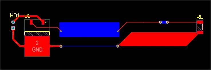
The base circuit's PCB layout, with a range of copper shapes and traces connected by layers and vias.
The PDN Analyzer panel interface (Tools » PDN Analyzer) visually emulates a Power Source to Load circuit net that incorporates tangible Power and Ground paths – much as shown in the above circuit and also the conceptual block diagram (Fig. 1). The application automatically extracts all physical and electrical information (netlist, devices and layer shapes, etc) from the currently active PCB design, which provides data for the PI-DC simulation engine.
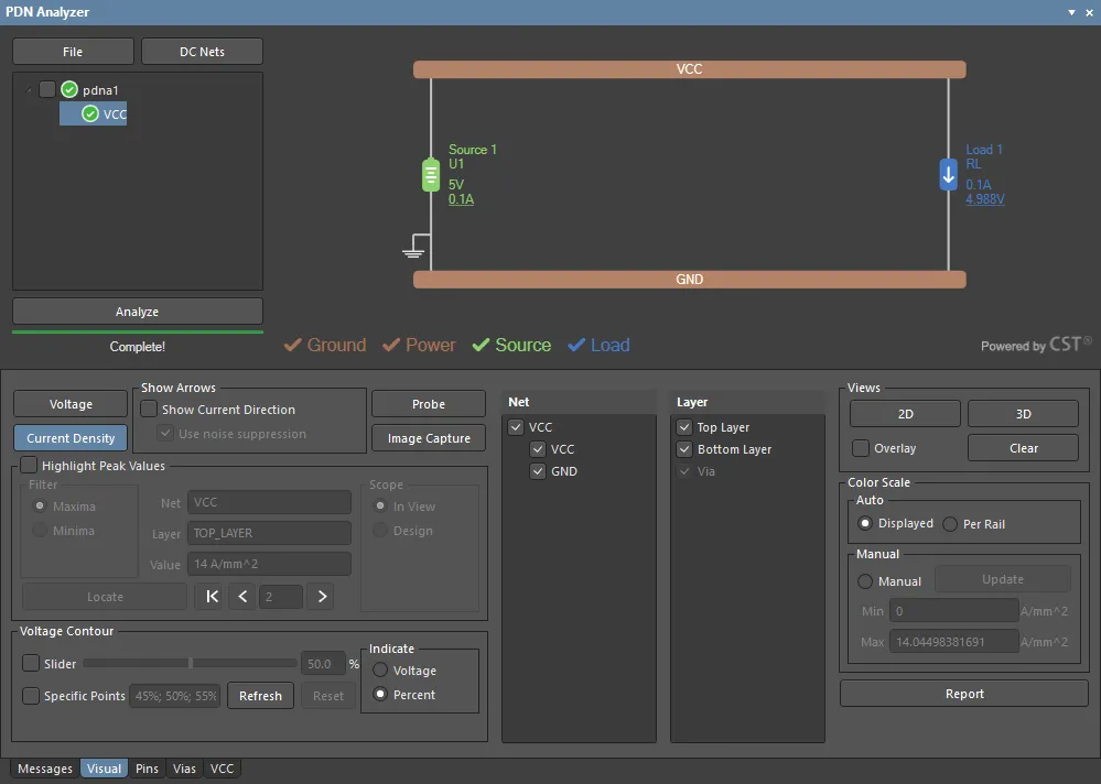
The PDN Analyzer panel interface showing a PI simulation setup for the basic circuit and board layout.
Here, the voltage source is the output of U1 (5V between pins 3 and 2), and the load is a specified current through RL (0.1A). Once the initial parameters have been entered via the interface (source/load voltages and currents, etc) and the simulation has been run, the resulting analysis data is graphically modeled in the PCB editor as a rendered 2D or 3D image.
 The Voltage Drop simulation results for the board's PWR and GND nets copper (U1 to RL, and RL to U1).
The PDN Analyzer PI simulation can be set to show Voltage (IR Drop, above image) or Current Density (below image) results for all applicable board layers.

The Current Density map for both the PWR and GND nets (U1 to RL).
► See the PDN Analyzer example guide for a complete description of using the PDN Analyzer and interpreting its results.

