
Additional Views
Along with the board assembly view and the board fabrication view, Draftsman suggests several additional automated design views to complete your PCB drawing.
Board Section View
A Draftsman board section view provides a profile slice, or sectional, drawing taken from a nominated 'cut' point through a placed board assembly view. The section view generator takes the available 3D data from the current PCB to create a standalone section drawing aligned to the nominated cut point.

Two placed board section views applied to a board assembly view
The steps to create a board section view are:
-
Select the board section view placement command (Place » Additional Views » Board Section View).
-
Position the cursor on a board assembly view, where a vertical cut line will follow the cursor movement. Use the
Spacebarto toggle between vertical and horizontal cut lines. -
Click to set the position of the cut line.
-
Move the cursor on either side of the line to set the view direction (as indicated by the cut line arrows) and click to confirm.
-
Drag and place the new board section view in the desired location.
The position, size, and target point of a placed board section view may be graphically modified when it has been selected in the design space. The view allows for different modes of graphic editing:
-
Click, Hold&Dragthe board section view graphic to change its location. -
Click, Hold&Dragthe board section view's scaling handle (node), located at the top right of its outline, to modify the view's rendered size. -
Click, Hold&Dragthe board section view's cutting line (away from its nodes) to change the position of the cut through the board. -
Click, Hold&Dragone of the board section view's cutting line nodes to change the extents of the cut through the board. -
When dragging the cutting line or its node, use the
Spacebarto change the Positioning Mode (Horizontal or Vertical).
Demonstration of board section view placement and graphical editing
Drawing representation, view direction, and labeling of a placed board section view are configurable in the Properties panel when the view is selected in the design space (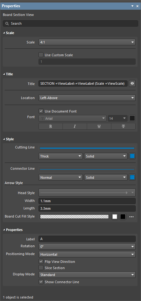 ).
).
Scale |
|
| Scale, Use Custom Scale |
Use these options to configure the view's scale. For more information, refer to the Working with Views page. |
Title |
|
| Title, Location, Font |
Use these options to configure the view's title. For more information, refer to the Working with Views page. |
Style |
|
| Cutting Line | Use the drop-downs to select the line thickness and pattern used to render the view's arrowed indicator lines. Available options are defined in the Line Styles region of the Properties panel when no object is selected in the design space. For more information, refer to the Setting Up a Draftsman Document page. Use the associated color button to specify the color of the line. |
| Connector Line | Use the drop-downs to select the line thickness and pattern used to render the view's cutting line, which lies between the arrowed section indicators (and passes through the board assembly view). Available options are defined in the Line Styles region of the Properties panel when no object is selected in the design space. For more information, refer to the Setting Up a Draftsman Document page. Use the associated color button to specify the color of the line. |
| Arrow Style | Use the provided options to configure the section indicator.
|
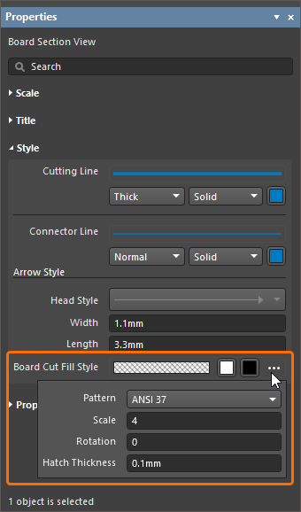
| Board Cut Fill Style | Use these options to configure the display of the graphic fill pattern and color of the sectioned (cut) board. The pattern swatch shows the preview of the pattern according to the configured settings. Use the associated color buttons to specify colors for the fill and hatch pattern. Select the associated
|
Properties |
|
| Label | The text string/character used for the view label name displayed as the section cut label. |
| Rotation | The angle of rotation, relative to the source board assembly view at which the board section view is rendered. Use the drop-down menu to choose from the sequence of 90° presets. |
| Positioning Mode | The X/Y orientation of the section cut, either Horizontal or Vertical. |
| Flip View Direction | When enabled, the section view orientation (the direction from which it is 'viewed') is inverted. The cut line direction arrows will change accordingly. |
| Slice Section | When enabled, the visibility of objects behind the cut line is disabled. It removes the background objects from the view, creating a literal cut view through the board ( ). ). |
| Display Mode | The display style of the cut indicator arrows, so they are positioned either after (Standard) or before (Alternative) the cut line ( ). ). |
| Show Connector Line | When enabled, the visibility of the cut line is enabled. |
 )
)Board Detail View
The Draftsman board detail view feature allows a defined area of a drawing to be brought out to a floating, magnified view of its detail. Board detail views can be added to a board assembly view, board fabrication view, board section view, component view, drill drawing view, board isometric view, and board region view. A board detail view can be created with either a circle or rectangular shape.
 applied to a board assembly view and a board fabrication view")
Two placed board detail views (at the bottom) applied to a board assembly view and a board fabrication view
The steps to create a board detail view are:
-
Select a board detail view placement command (Place » Additional Views » Board Detail View » Circle area detail view or Place » Additional Views » Board Detail View » Rectangle area detail view, depending on which shape of the view is required).
-
Click at a point on the drawing (on a supported view) to specify the center of the target board detail view area.
-
Move the mouse then click to specify the radius (for a circle shape view) / corner (for a rectangular shape view) of the view area (the board detail view source). The view will appear floating on the cursor.
-
Click again to set the position of the board detail view expansion.
Both the board detail view and its source area/size may be graphically modified. To enable its graphic editing mode, click on any part of the graphic representation, including the board detail view expansion, the perimeter of the source area, the label, or the connection/leader line.
-
Click, Hold&Dragthe board detail view itself (the magnified view of the source area) to change its location. -
Hover the cursor over the label or connection/leader line (the cursor will change to a 'move' crosshair –
 ), then
 Click, Hold&Dragto move the view's source area position. -
Hover the cursor over the source area outline (the cursor will change to a 'resize' crosshair –
 ), then
 Click, Hold&Dragto change the view's source area size. -
If the board detail view object uses a label leader (Display Mode set to With Leader in the Properties panel), it will show an editing handle that may be dragged to reposition the leader and its label.
Demonstration of board detail view placement and graphical editing
The magnification factor (scale), labeling, and line attributes of a placed board detail view are configurable in the Properties panel when the view is selected in the design space (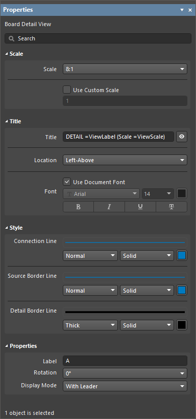 ).
).
Scale |
|
| Scale, Use Custom Scale |
Use these options to configure the view's scale. For more information, refer to the Working with Views page. |
Title |
|
| Title, Location, Font |
Use these options to configure the view's title. For more information, refer to the Working with Views page. |
Style |
|
| Connection Line | Use the drop-downs to select the line thickness and pattern used to render the leader label line (when the Display Line option is set to With Leader) or the line that connects the source outline and the view itself (when the Display Line option is set to Connected). Available options are defined in the Line Styles region of the Properties panel when no object is selected in the design space. For more information, refer to the Setting Up a Draftsman Document page. Use the associated color button to specify the color of the line. |
| Source Border Line | Use the drop-downs to select the line thickness and pattern used to render the view's source area outline. Available options are defined in the Line Styles region of the Properties panel when no object is selected in the design space. For more information, refer to the Setting Up a Draftsman Document page. Use the associated color button to specify the color of the lines. |
| Detail Border Line | Use the drop-downs to select the line thickness and pattern used to render the view's magnified area outline. Available options are defined in the Line Styles region of the Properties panel when no object is selected in the design space. For more information, refer to the Setting Up a Draftsman Document page. Use the associated color button to specify the color of the line. |
Properties |
|
| Label | The text string/character used for the view label name. It is displayed as the view label when the Display Line option is set to With Leader or No Leader. |
| Rotation | The angle at which the magnified area is shown, where 0° relates to the area's inherent view angle in the source (target) drawing view. Choose from a sequence of 90° view options in the drop-down menu. |
| Display Mode | The style of connection line for the view source. Use the drop-down to select the Connected, With Leader, or No Leader style (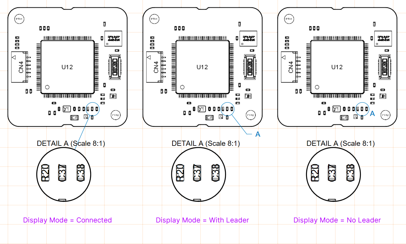 ). ). |
Component View
A Draftsman component view (Place » Additional Views » Component View) is an assembly view-style drawing object of a single component from the current board design. When set as a profile view, the rendered component view includes the related profile section of the supporting PCB.

Two placed component views that show a component from the top and front sides
A placed component view will initially show the first component registered in the BOM data. This can be changed to the desired component from the Component drop-down in the Properties region of the Properties panel, which also offers the property settings that define the component view's graphic style and view angle (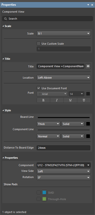 ).
).
Scale |
|
| Scale, Use Custom Scale |
Use these options to configure the view's scale. For more information, refer to the Working with Views page. |
Title |
|
| Title, Location, Font |
Use these options to configure the view's title. For more information, refer to the Working with Views page. |
Style |
|
| Board Line | Use the drop-downs to select the line thickness and pattern used to render the board line when the View Side is set to a value other than Top. Available options are defined in the Line Styles region of the Properties panel when no object is selected in the design space. For more information, refer to the Setting Up a Draftsman Document page. Use the associated color button to specify the color of the line. |
| Component Line | Use the drop-downs to select the line thickness and pattern used to render the component geometry in the view. Available options are defined in the Line Styles region of the Properties panel when no object is selected in the design space. For more information, refer to the Setting Up a Draftsman Document page. Use the associated color button to specify the color of the lines. |
| Distance To Board Edge | When the View Side is set to a value other than Top, specifies the distance from the component view to the edge of the board. |
Properties |
|
| Component | The board design component that will be rendered in the view. Use the drop-down menu to select from the list of all available component designators. |
| View Side | The direction of view used to render the component drawing. Use the drop-down menu to select from a range of preset view directions. |
| Rotation | The angle of rotation used to render the view, as applied by the drop-down menu. |
| Show Pads | Options in this region are available only when the View Side for the selected component view is set to Top. Enabled SMD and/or Through-Hole option to render respective pad shapes in the view. Select the associated color button to specify the pad display color. |
 ).
).Drill Drawing View
A Draftsman drill drawing view (Place » Additional Views » Drill Drawing View) is an automated graphic composite of the active PCB project's board outline and drill holes. The view is rendered with definable symbols that correspond to hole types and also includes any specified drill layer pairs.

A placed drill drawing view can show holes for all or specific drill pairs and rendered with defined hole group symbols.
A placed drill drawing view will initially show drill pairs for all layers. This can be changed after placement as required, through the Properties panel, which also offers the property settings that define the drill drawing view's side and assigned drill symbol graphics for the various drill holes (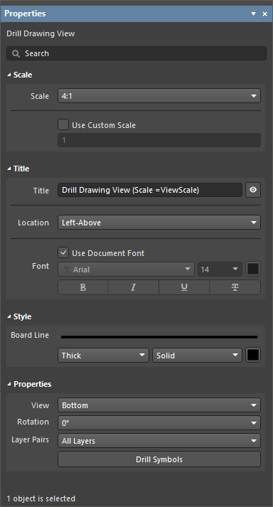 ).
).
Scale |
|
| Scale, Use Custom Scale |
Use these options to configure the view's scale. For more information, refer to the Working with Views page. |
Title |
|
| Title, Location, Font |
Use these options to configure the view's title. For more information, refer to the Working with Views page. |
Style |
|
| Board Line | Use the drop-downs to select the line thickness and pattern used to render the view's border/outline. Available options are defined in the Line Styles region of the Properties panel when no object is selected in the design space. For more information, refer to the Setting Up a Draftsman Document page. Use the associated color button to specify the color of the line. |
Properties |
|
| View | The direction of view used to render the view. Use the drop-down menu to specify the Top or Bottom view direction. |
| Rotation | The angle of rotation used to render the view, as applied by the drop-down menu. |
| Layer Pairs | Select which PCB drill layer pair holes will be displayed in the drawing view. Use the drop-down menu to choose from the layer pairs that are available in the source board design as can be viewed and edited in the PCB editor's Layer Stack Manager. All board designs will have a Top Layer to Bottom Layer pair, while other pairs will represent via holes passing between or to other layers, such as internal/plane layers. For more information, refer to the Blind, Buried & Micro Via Definition page. |
| |
Click the button to open the Drill Symbol Configurations dialog, which provides a tabular view of all drill hole data, with hole styles grouped on a selectable parameter (column data) basis and assigned standard symbols. The dialog allows the setting of the style and size for each hole symbol. |
Board Isometric View
A Draftsman board isometric view (Place » Additional Views » Board Isometric View) is an automated projection graphic composite of the active PCB project's board assembly.

Two placed board isometric views; a front face view on the left and a top face view on the right
The settings for a placed board isometric view, including its face side and design variant, are available in the Properties panel when the view is selected in the design space (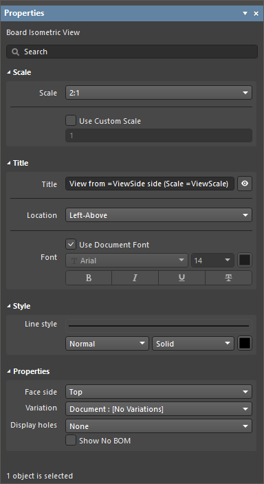 ).
).
Scale |
|
| Scale, Use Custom Scale |
Use these options to configure the view's scale. For more information, refer to the Working with Views page. |
Title |
|
| Title, Location, Font |
Use these options to configure the view's title. For more information, refer to the Working with Views page. |
Style |
|
| Line Style | Use the drop-downs to select the line thickness and pattern used to render the view's board outline and component geometry. Available options are defined in the Line Styles region of the Properties panel when no object is selected in the design space. For more information, refer to the Setting Up a Draftsman Document page. Use the associated color button to specify the color of the line. |
Properties |
|
| Face side | The direction of the isometric projection used to render the view. Use the drop-down menu to select from a range of preset view directions. |
| Variation | The design variant, for which the view shows its data. Components set as not fitted for the selected variant are not rendered in the view. |
| Display holes | Use the drop-down to select the desired holes display option: None, All, or Pads only. |
| Show No BOM | Use this option to toggle the display of no BOM components (whose Type is set to Standard (No BOM) in the PCB editor) in the view. |
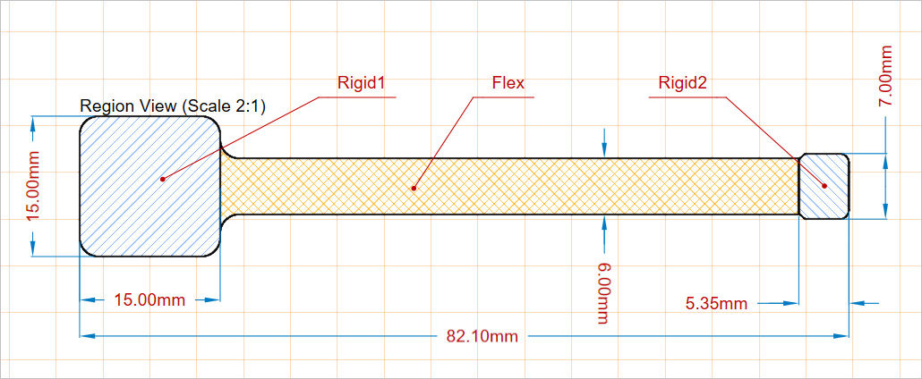
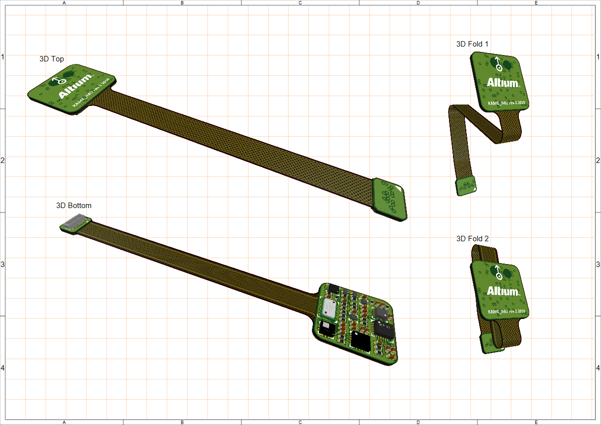
Board Region View
The board region view (Place » Additional Views » Board Region View) allows a Draftsman document to include an accurate representation of multiple layer stack regions in a board design, such as those applied in rigid-flex PCB designs. Layer stack naming and data applied in the view are drawn from the PCB design, as represented in the PCB editor’s Board Planning Mode view and Layer Stack Manager.

A placed board region view
The settings for a placed board region view are available in the Properties panel when the view is selected in the design space (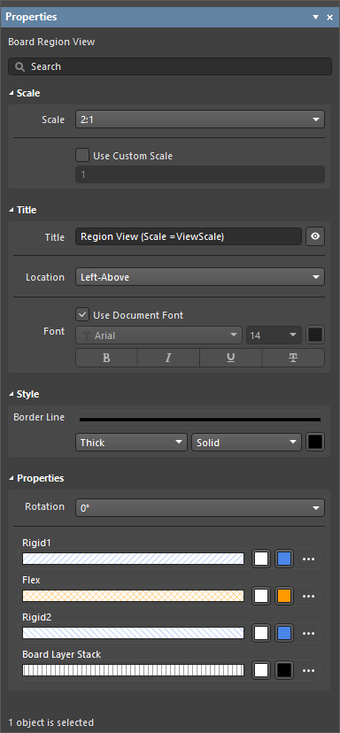 ).
).
Scale |
|
| Scale, Use Custom Scale |
Use these options to configure the view's scale. For more information, refer to the Working with Views page. |
Title |
|
| Title, Location, Font |
Use these options to configure the view's title. For more information, refer to the Working with Views page. |
Style |
|
| Border Style | Use the drop-downs to select the line thickness and pattern used to render the view's board outline. Available options are defined in the Line Styles region of the Properties panel when no object is selected in the design space. For more information, refer to the Setting Up a Draftsman Document page. Use the associated color button to specify the color of the line. |
Properties |
|
| Rotation | The angle of rotation used to render the view, as applied by the drop-down menu. |
| Region graphic properties | For each of the board's layer stack regions, an entry that allows configuring its associated graphic properties is included. The pattern swatch shows the preview of the pattern according to the configured settings. Use the associated color buttons to specify colors for the fill and hatch pattern. Select the associated
|
 )
)
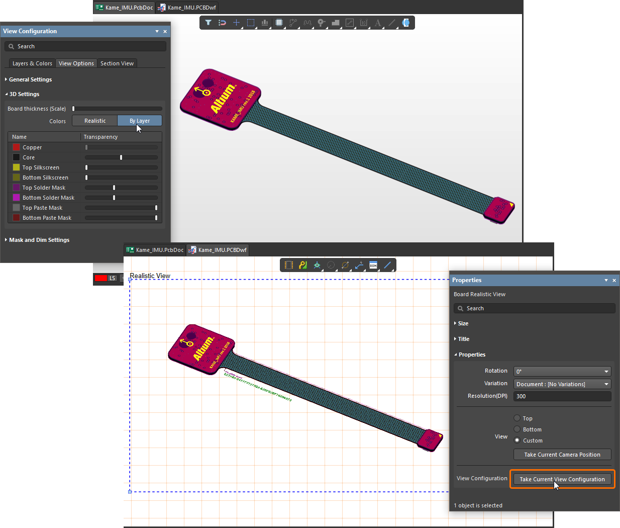
Board Realistic View
A Draftsman board realistic view (Place » Additional Views » Board Realistic View) provides a high level of purely visual information of the assembly and fabrication data in a drawing document. Placed as a separate and configurable view object, the board realistic view provides a scalable 3D rendering of the current board design. The 3D view is generated by the software’s 3D rendering engine – as applied in the PCB editor – and may be set to adopt the PCB editor’s current view angle and configuration.

A placed board realistic view. The view angle has been taken from the PCB editor.
The settings for a placed board realistic view are available in the Properties panel when the view is selected in the design space (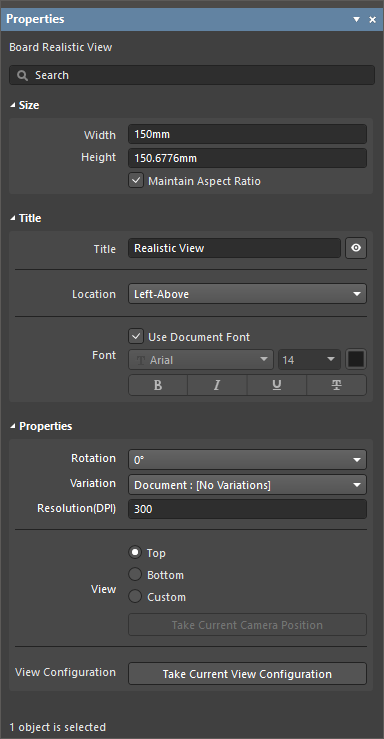 ).
).
Size |
|
| Width | The width of the view. |
| Height | The height of the view. |
| Maintain Aspect Ratio | When this option is enabled, the image dimensions will remain in proportion when the object is scaled by entering a new Width or Height or by dragging the object's selection nodes in the design space. |
Title |
|
| Title, Location, Font |
Use these options to configure the view's title. For more information, refer to the Working with Views page. |
Properties |
|
| Rotation | The angle of rotation used to render the view, as applied by the drop-down menu. |
| Variation | The design variant, for which the view shows its data. Components set as not fitted for the selected variant are not rendered in the view. |
| Resolution(DPI) | The quality of the view in terms of resolution. The minimum setting is 75 DPI. |
| View | Select Top or Botton to render the view from the corresponding side of the source board design or select Custom to enable the 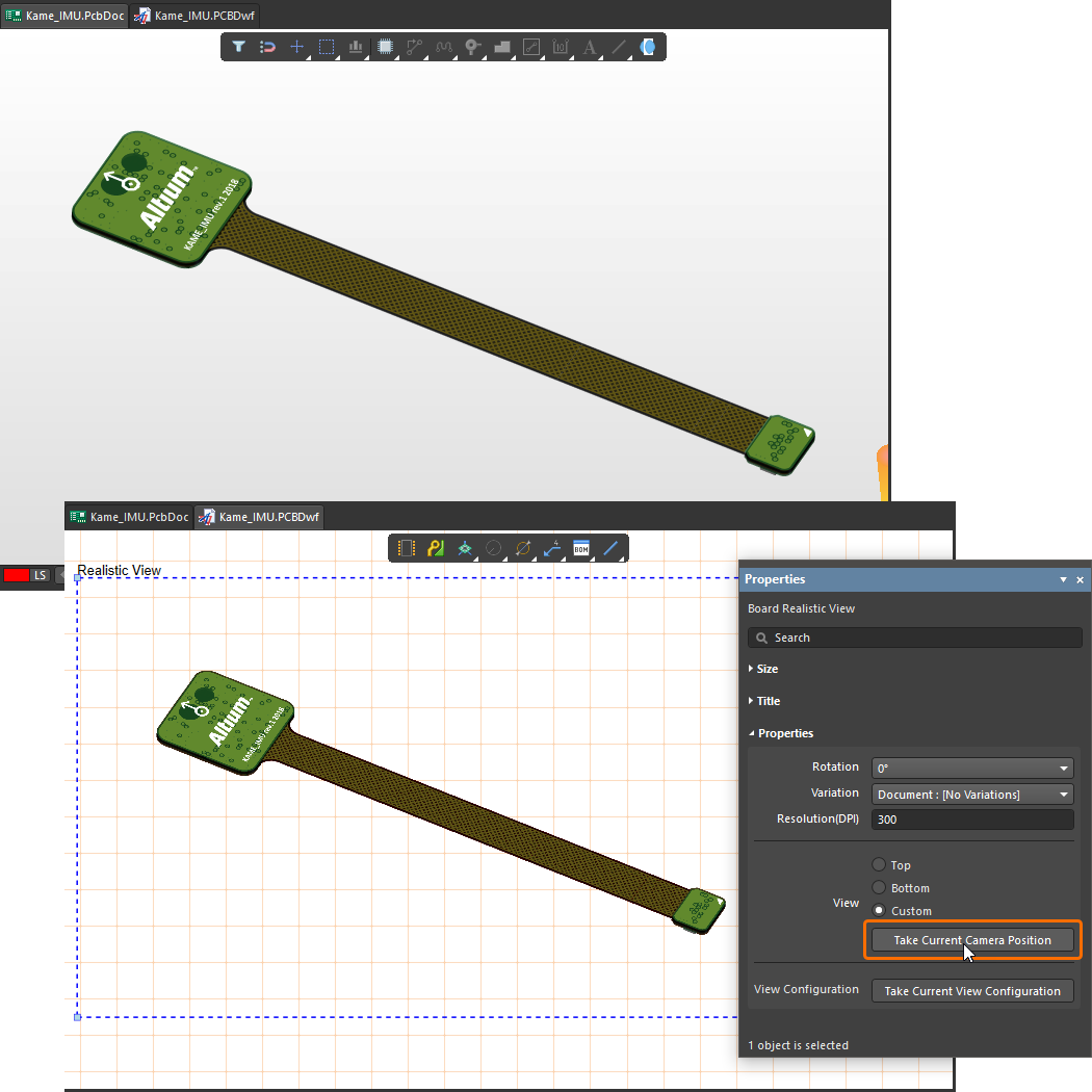 ). ). |
| View Configuration | Click the |
 ).
).
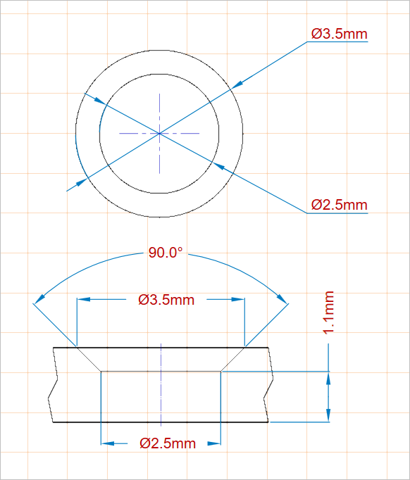
Counter Hole View
A Draftsman counter hole view (Place » Additional Views » Counter Hole View) provides a representation of a board's pad hole with counter hole features (counterbore and/or countersink). When set as a profile view, the rendered counter hole view includes the corresponding profile section of the PCB.

Two placed counter hole views that show a pad hole from the top and left sides
A placed counter hole view will initially show the hole of one of the PCB pads with a counter hole feature applied. This can be changed to the required pad from the Properties panel, which also offers the property settings that define the view's graphic style and view side (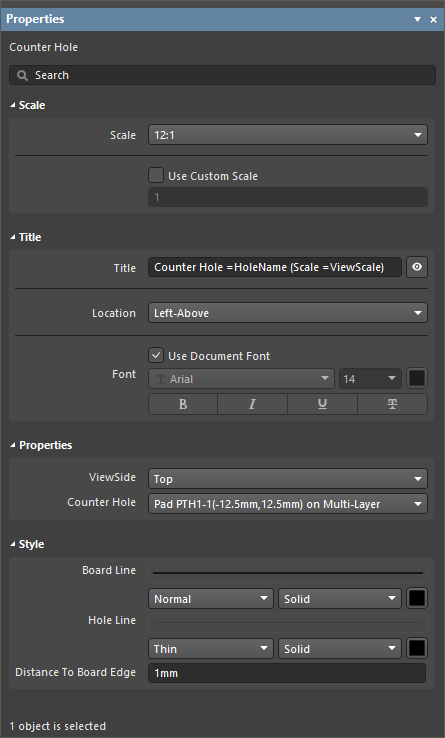 ).
).
Scale |
|
| Scale, Use Custom Scale |
Use these options to configure the view's scale. For more information, refer to the Working with Views page. |
Title |
|
| Title, Location, Font |
Use these options to configure the view's title. For more information, refer to the Working with Views page. |
Properties |
|
| ViewSide | The direction of view used to render the hole drawing. Use the drop-down menu to select from a range of preset view directions. |
| Counter Hole | The board design pad with a counter hole feature applied which hole will be rendered in the view. Use the drop-down menu to select from the list of all available counter holes. |
Style |
|
| Border Line | Use the drop-downs to select the line thickness and pattern used to render the view's board line (applies when the ViewSide is set to Left). Available options are defined in the Line Styles region of the Properties panel when no object is selected in the design space. For more information, refer to the Setting Up a Draftsman Document page. Use the associated color button to specify the color of the line. |
| Hole Line | Use the drop-downs to select the line thickness and pattern used to render the view's hole geometry. Available options are defined in the Line Styles region of the Properties panel when no object is selected in the design space. For more information, refer to the Setting Up a Draftsman Document page. Use the associated color button to specify the color of the line. |
| Distance To Board Edge | When the ViewSide is set to Left, specifies the distance from the hole view to the edge of the board. |
Via Type View
A Draftsman via type view (Place » Additional Views » Via Type View) represents a via type according to the IPC-4761 standard, Design Guide for Protection of Printed Board Via Structures.
")
A placed via type view that illustrates a Type 3A via (sealing with a non-conductive material on one side, which partially enters the via)
The settings for a placed via type view, including the shown via type and the view's graphic style, are available in the Properties panel when the view is selected in the design space ( ).
).
Scale |
|
| Scale, Use Custom Scale |
Use these options to configure the view's scale. For more information, refer to the Working with Views page. |
Title |
|
| Title, Location, Font |
Use these options to configure the view's title. For more information, refer to the Working with Views page. |
Properties |
|
| Via Type | The via type according to the IPC-4761 standard used to render the via drawing. Use the drop-down menu to select from a range of preset via types. |
| Side | Use the drop-down to select from what side covering should be applied. For via types 1A, 2A, 3A, 4A, and 6A, choose from either Top or Bottom. For via types 1B, 2B, 3B, 4B, 5, 6B, and 7, the option is effectively disabled with Both as the only option and is the default for those via types. |
| Layer Stack | The PCB design layer stack, as defined in the PCB editor's Layer Stack Manager, according to which the view will be rendered. Use the drop-down menu to select from the list of all available layer stacks. |
Style |
|
| Line Style | Use the drop-downs to select the line thickness and pattern used to render the view's outline lines. Available options are defined in the Line Styles region of the Properties panel when no object is selected in the design space. For more information, refer to the Setting Up a Draftsman Document page. Use the associated color button to specify the color of the line. |
| Hole Fill Color | Use the associated color button to specify the color used to render the view's hole fill. |
| Plug Color | Use the associated color button to specify the color used to render the view's plug. |
| Cover Color | Use the associated color button to specify the color used to render the view's cover. |

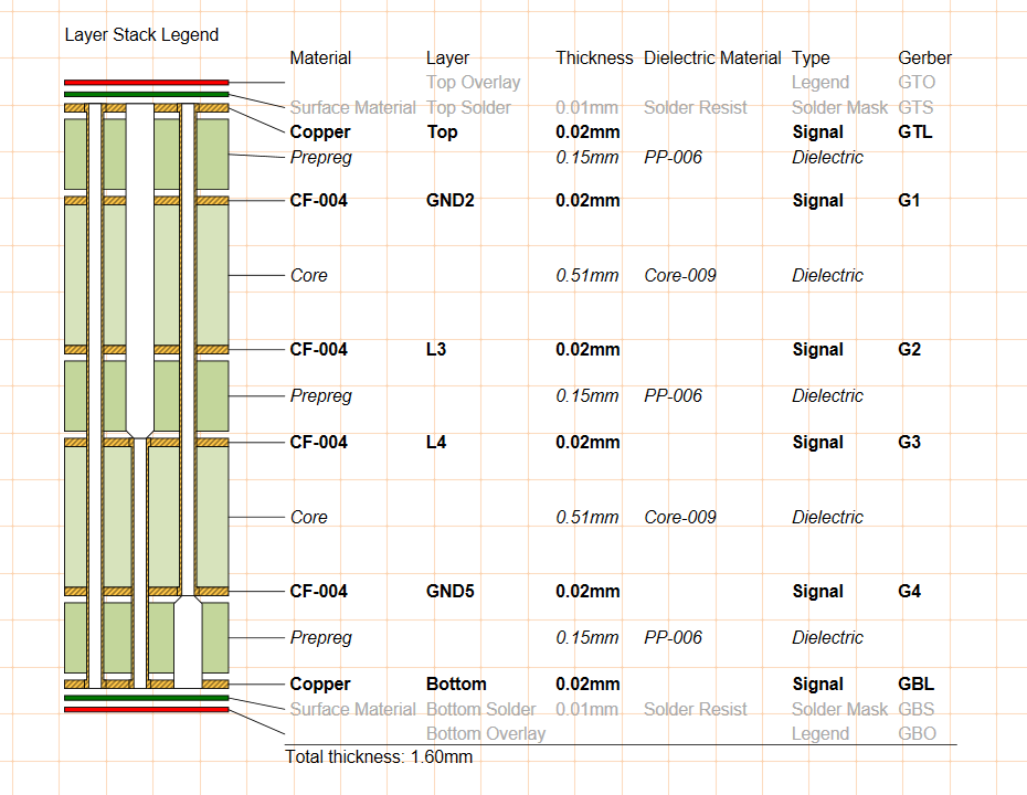
Layer Stack Legend
A Draftsman layer stack legend view (Place » Layer Stack Legend) provides a representation of the board's internal structure as an enlarged sectional view. It includes detailed descriptions and information for each layer in the stack, including the Gerber files associated with each layer.

A placed layer stack legend derives data from the layer stack for the source PCB and can be displayed with relative layer thickness and via types.
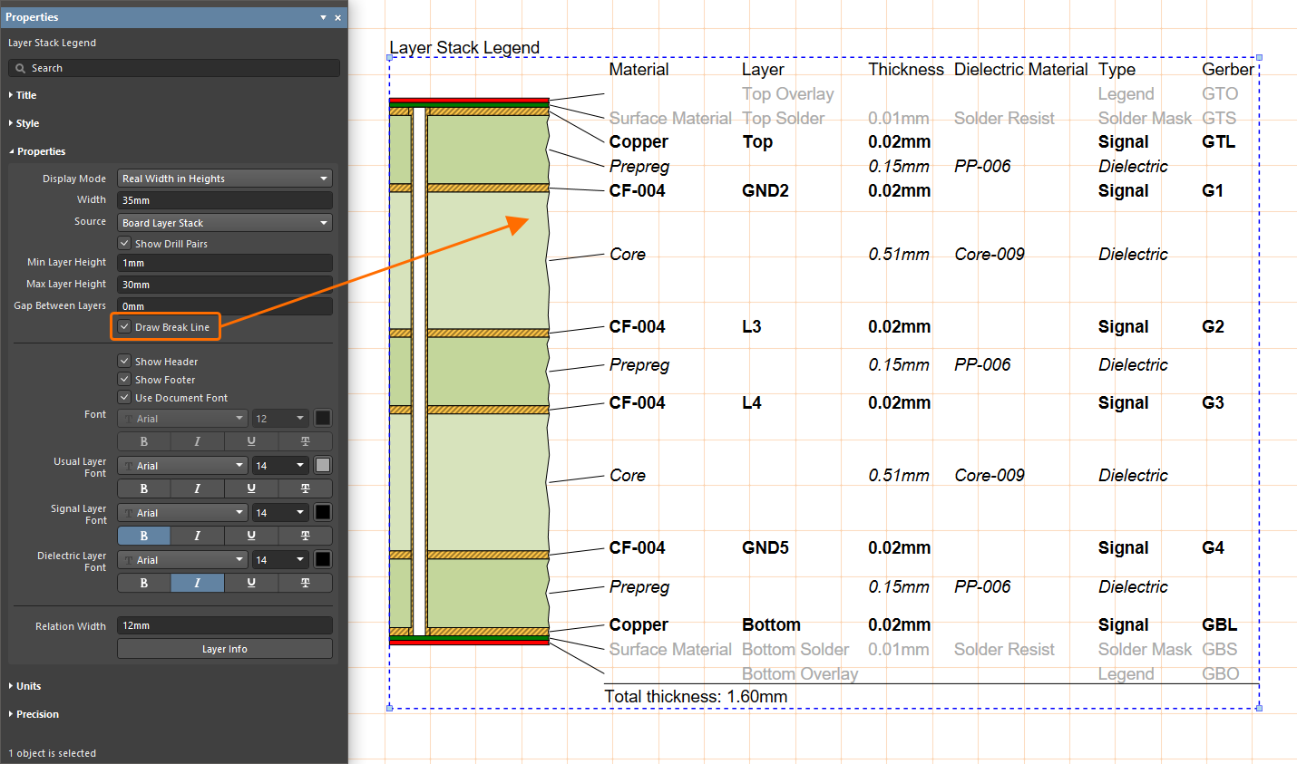
By default, the information for each layer is derived from the corresponding attributes in the board layer stack, as defined in the PCB editor's Layer Stack Manager. However, the layer description attributes may be edited and expanded in Draftsman through the Properties panel when the view is selected in the design space (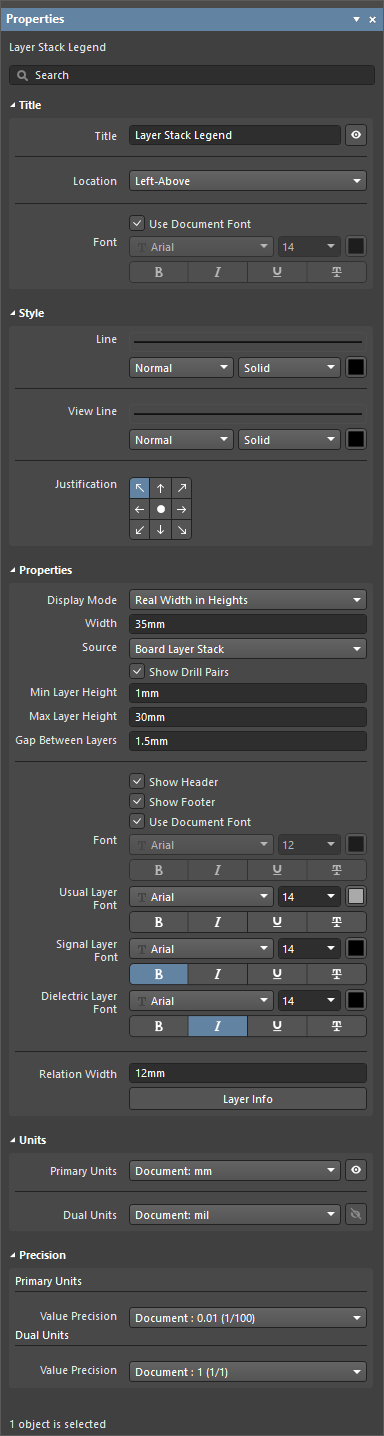 ).
).
Title |
|
| Title, Location, Font |
Use these options to configure the view's title. For more information, refer to the Working with Views page. |
Style |
|
| Line | Use the drop-downs to select the line thickness and pattern used to render the view's line between each layer representation and its corresponding specification table row. Available options are defined in the Line Styles region of the Properties panel when no object is selected in the design space. For more information, refer to the Setting Up a Draftsman Document page. Use the associated color button to specify the color of the line. |
| View Line | Use the drop-downs to select the line thickness and pattern used to render the view's layer representation outlines. Available options are defined in the Line Styles region of the Properties panel when no object is selected in the design space. For more information, refer to the Setting Up a Draftsman Document page. Use the associated color button to specify the color of the line. |
| Justification | Select the point relative to which the position of the view is changed if its size is updated. |
Properties |
|
| Display Mode | Determines the rendered height of each layer representation in the view's graphic within the constraints of the Min Layer Height and Max Layer Height settings. Use the drop-down to choose the layer heights option:
|
| Width | Sets the rendered width of the view's graphic. The minimum width is determined by the number of via types included. |
| Source | The PCB design layer stack, as defined in the PCB editor's Layer Stack Manager, used as the data source for the view. |
| Show Drill Pairs | Enables a graphic representation of the drill layer pairs (via types), as defined in the PCB editor's by the PCB project's Layer Stack Manager (learn more about Blind, Buried & Micro Via Definition). |
| Min Layer Height | The minimum rendered height of any layer. This setting will only influence the graphic when the Display Mode option is set to Real Width in Heights. |
| Max Layer Height | The maximum rendered height of any layer. This setting will only influence the graphic when the Display Mode option is set to Real Width in Heights. |
| Gap Between Layers | Sets the amount of free space desired between layer graphics. |
| Show Header | Enable/disable the column header captions in the view's table. |
| Show Footer | Enable/disable the total board thickness readout at the bottom of the view's table. |
| Font | Sets the header and footer font used in the view's table.
|
| Usual Layer Font | Sets the font used for the table information that relates to the board's outer/surface layers, such as the paste, silkscreen, and solder layers. Use the provided options to choose the desired font type, size, color, and text attributes. |
| Signal Layer Font | Sets the font used for the table information that relates to the board's copper signal-carrying layers, such as the top/bottom and internal/plane layers. Use the provided options to choose the desired font type, size, color, and text attributes. |
| Dielectric Font | Sets the font used for the table information that relates to the board's dielectric core layers. Use the provided options to choose the desired font type, size, color, and text attributes. |
| Relation Width | Sets the distance between the layers graphic and the table, and by association the length of the layer to table row indicator lines. |
| |
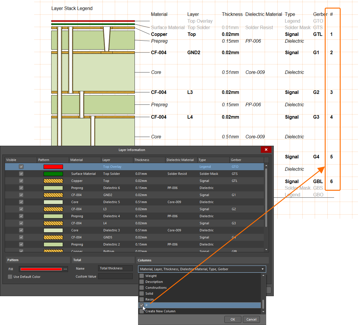
Click the button to open the Layer Information dialog – see below. |
Units |
|
| Primary Units | Select the primary measurement unit type that will be shown in the view's table. Use the associated |
| Dual Units | Select the secondary (dual) measurement unit type that will be shown in the view's table. Use the associated |
Precision |
|
| Primary Units | Use the Value Precision drop-down menu to set the precision accuracy definition (up to five digits to the right of the decimal point, with the last digit rounded) for the primary layer dimension table entries. |
| Dual Units | Use the Value Precision drop-down menu to set the precision accuracy definition (up to five digits to the right of the decimal point, with the last digit rounded) for the dual layer dimension table entries, if enabled. |
 ).
). ).
).The Layer Information dialog accessed by clicking the ![]() button in the Properties panel when the layer stack legend is selected in the design space allows the editing of the layer stack legend's table data and graphics color/visibility.
button in the Properties panel when the layer stack legend is selected in the design space allows the editing of the layer stack legend's table data and graphics color/visibility.
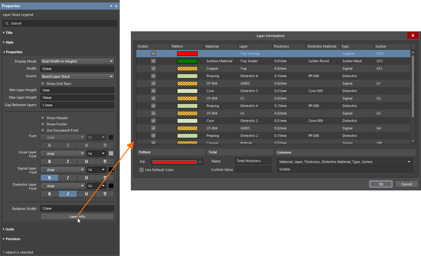
| Grid | Displays information for each layer in the design, the defaults being Material, Layer, Thickness, Dielectric Material, Type, and Gerber. |
| Pattern |
|
| Total |
|
| Columns | Use the drop-down to enable or disable the checkbox next to entries to show/hide corresponding columns in the table. |
 ).
). ).
).