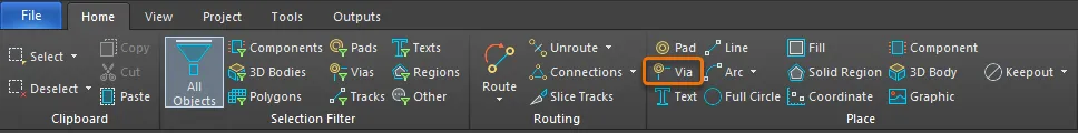
비아는 PCB 편집기와 PCB 라이브러리 편집기에서 다음과 같은 방식으로 배치할 수 있습니다.
- PCB 편집기에서는 메인 메뉴에서 Home | Place | Via를 선택합니다.
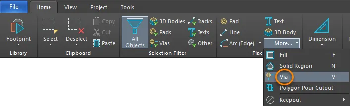
- PCB 라이브러리 편집기에서는:
- 메인 메뉴에서 Home | Place | More » Via 를 선택합니다.
- 디자인 공간에서 마우스 오른쪽 버튼을 클릭한 다음 Place » Via.
를 선택합니다. 명령을 실행하면 커서가 십자선으로 바뀌고 비아 배치 모드로 들어갑니다:
- 커서를 위치시키고 클릭하거나 Enter를 눌러 비아를 배치합니다.
- 추가 비아를 계속 배치하거나, 마우스 오른쪽 버튼을 클릭하거나 Esc를 눌러 배치 모드를 종료합니다.
비아는 이미 넷에 연결된 객체 위에 배치되면 해당 넷 이름을 채택합니다. 일반적으로 비아는 수동으로 배치하지 않으며, 대화형 라우팅 과정의 일부로 자동 배치됩니다.
라우팅 중 비아 자동 배치
넷을 대화형으로 라우팅하는 동안 숫자 키패드의 * 키를 눌러 사용 가능한 신호 레이어를 순환할 수 있습니다. 또는 Ctrl+Shift+Roll Mouse Wheel 조합을 사용해 신호 레이어를 이동할 수 있습니다. 이렇게 하면 소프트웨어가 적용 가능한 Routing Via Style 설계 규칙에 따라 비아를 자동으로 배치합니다. 서로 다른 넷에 서로 다른 비아 크기를 할당할 수 있도록 여러 개의 Via Style 설계 규칙을 정의할 수 있다는 점에 유의하십시오.
기본 설정 vs 설계 규칙
비아를 빈 공간에 배치하는 경우, 소프트웨어가 배치 중 라우팅 스타일 설계 규칙을 적용할 수 없습니다. 이 상황에서는 기본 비아가 배치됩니다.
그래픽 편집
비아는 위치를 제외하고는 그래픽 방식으로 속성을 수정할 수 없습니다. 비아를 이동하면서 연결된 트랙도 함께 이동하려면, 비아를 클릭한 채로 유지한 다음 이동하십시오. 이동하는 동안 연결된 라우팅은 비아에 계속 붙어 있습니다.
라우팅 또는 부품 공간을 더 확보하기 위해 라우팅과 함께 비아를 이동하는 경우, 라우팅을 이동하는 것보다 재라우팅이 더 효율적일 수 있습니다. 소프트웨어에는 Automatically Remove Loops라는 기능이 있으며, PCB Editor - Interactive Routing System Preferences dialog의 페이지에서 활성화할 수 있습니다. 이 기능을 활성화하면 (기존 라우팅의 중간에서 시작해 중간에서 끝나는 방식으로) 새 경로를 따라 라우팅하고, 대화형 라우팅 모드를 종료하기 위해 마우스 오른쪽 버튼을 클릭하는 즉시 기존 라우팅(루프)이 제거되며, 중복 비아도 함께 제거됩니다.
객체 선택을 해제(또는 선택 해제)하려면 Esc 키를 사용합니다.
비-그래픽 편집
이 편집 방법은 Inspector 패널 모드를 사용하여 Via 객체의 속성을 수정합니다.
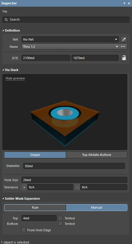
배치 중에는 Inspector 패널의 Via 모드를 Tab 키를 눌러 접근할 수 있습니다. 비아를 배치하면 모든 옵션이 표시됩니다.
배치 후에는 Inspector 패널의 Via 모드를 다음 방법 중 하나로 접근할 수 있습니다:
- Inspector 패널이 이미 열려 있다면, 비아 객체를 선택하고 마우스 오른쪽 버튼을 클릭한 다음 컨텍스트 메뉴에서 Properties 를 선택합니다.
- 비아를 선택한 상태에서 메인 리본에서 View | Schematic | Inspector 를 선택합니다.

 AI로 번역됨