Summary
The SCHLIB List panel allows you to display design objects associated with one or more schematic components in tabular format, enabling you to quickly inspect and/or modify object attributes. When used in conjunction with the SCHLIB Filter panel panel, it enables you to display just those objects falling under the scope of the active filter, allowing you to target and edit multiple design objects with greater accuracy and efficiency.
Panel Access
The panel can be accessed from the schematic library editor in the following ways:
- Click Panels at the bottom-right of the workspace then select SCHLIB List from the pop-up menu.
- Click View » Panels » SCHLIB List.
- Use the Shift+F12 shortcut keys.
Panels can be configured to be floating in the editor space or docked to sides of the screen. If the SCHLIB List panel is currently in a group of panels, use the SCHLIB List tab located at the bottom of the panels to bring it to the front.
Content and Use
The panel is divided into two main regions:
- Filtering controls to define which objects are displayed in the panel (display scope).
- A tabular, spreadsheet-like region listing all objects falling under the defined display scope.
Defining Panel Display Scope
Controls at the top of the panel allow you to filter which objects are displayed in the panel and also control the current mode of the panel - allowing you to enable/disable the panel's direct editing functionality.

Click on the leftmost underlined control to select from the following options:
- View - in this mode, you will be able only to use the panel for viewing object attributes. You will not be able to edit any of the attribute fields in the tabular region of the panel.
- Edit - in this mode, you will be able to view and edit the attributes of design objects, directly in the tabular region of the panel.
Click on the next underlined control to select from the following options:
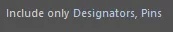
- non-masked objects - this is the default option and causes the panel to display only design objects that are not masked-out in the workspace (i.e. those objects that fall under the scope and specific query expression of the currently applied filter). This option is most effective when filtering is applied to the workspace and the associated masking highlight option is enabled.
- selected objects - display only design objects that are currently selected.
- all objects - to display all design objects.
Click on the next underlined control to choose from the following options:
- current component - only display target objects from the active library component in the design editor window.
- all components - display target objects from all components contained in the active schematic library document.
The right-most underlined control allows you to determine the type of objects that can be displayed. Click on the control to reveal a selection pop-up.

Use the pop-up to choose which object types you want to include in the currently displayed list - either all objects or specific objects. To choose one or more specific object types, enable the Display only option then enable the checkbox next to the required object(s) in the list beneath. The list will contain only those object types currently displayed in the main spreadsheet region of the panel.
When enabling specific object types for display, the control will reflect the choice by listing the enabled types separated by commas.
Working with Filtered Objects
The main region of the panel displays all design objects passing the defined display scope for the panel in tabular format.
Object data is initially unsorted. Data may be sorted by any attribute by clicking on the header for that attribute's column. Clicking once will sort in ascending order; click again to sort in descending order.
Displaying Workspace Selection
As you select objects in the design workspace, the corresponding entries for those objects will appear selected in the list. A selected object is distinguished in the list by the use of a blue background for all of its cells.

Displaying Filtering Results
When a filter has been applied based on a query expression in the SCHLIB Filter panel, only those objects under the scope of the filter will be shown provided that:
- The Mask out option is enabled in the Filter area of the SCHLIB Filter panel.
- The Display option for the SCHLIB List panel is set to non-masked objects.
If the
Select option has been enabled also in the
Filter area of the
SCHLIB Filter panel, all filtered objects will appear selected in the list.
Using the Panel to Select Objects in the Workspace

As you select entries for design objects in the list, those objects will become selected in the design workspace. The list supports single or multiple selections, the latter using standard Ctrl + Click, Shift + Click and click and drag features.
Double-click on an entry to open the associated Properties panel for that object in which you can make changes as required.
Editing Object Attributes
Editing is possible only if the panel is in Edit mode. When the panel is configured in View mode, you only will be allowed to view object properties.
You can edit attributes of an object by editing the relevant entry in the panel. Click on a cell to focus it and then either right-click and choose Edit or click again to edit the attribute value directly. Depending on the attribute, you will either need to type a value, toggle a checkbox or select an option from a drop-down. The change will take effect once you press Enter or click outside of the field you are editing. This is one of the advantages of using the panel to edit object properties - the panel will remain open, allowing you to change attribute after attribute as needed without having to reopen the Properties panel each time.
Another advantage of using the panel for editing is that you can edit multiple objects from one place. Selected objects can be of the same or differing type. Those attributes that are common to all objects in the selection will be displayed in the panel. Select the required cells across all required objects for the shared attribute you want to modify. Then either right-click then choose the Edit command or press the F2 key (or the Spacebar). You will be able to edit the value for the chosen attribute with respect to the focused object in the selection. Click outside the attribute's cell or press Enter to effect the change, which will subsequently be applied to all remaining objects in the selection.
By using filtering, you can apply a query (an expression for the filter) to target a specific group of objects in one or more components in the active library and then use the SCHLIB List panel to edit the attributes for these multiple objects.
Editing Attributes with Smart Grid Paste Tools
There are two Smart Grid commands available as right-click options from the SCHLIB List panel. These commands allow you to import and create or update tabular data from any Windows-compliant tabular/spreadsheet data such as an Excel workbook or a table in a PDF document in the SCHLIB List panel.
The Smart Grid Paste command alters the value of existing objects from pasted tabular data and Smart Grid Insert creates new objects from the tabular data. The SCHLIB List panel must be in the Edit mode in order to have copy and paste commands enabled.
Using Smart Grid Paste Command
There are two main ways to update attributes of design objects using the Smart Grid Paste command: updating attributes one at a time with no header data and updating attributes as a group with header data.
You need to determine whether the tabular data has the Header Row or No Header Row. These options are located at the top right of the Smart Grid Paste dialog. If the tabular data has the header row, then you can map and update multiple attributes otherwise, you will need to do different attributes one by one.
For example, to change attributes as a group using the Smart Grid Paste tool, copy the data using the Copy With Header command from the right-click menu from the SCHLIB List panel then paste the tabular data including the header row into an Excel workbook. The updated tabular data from this workbook can then be pasted back into the same SCHLIB List panel using the Smart Grid Paste command. Make sure the selected entries in the SCHLIB List panel correspond to the pasted tabular data; however, you can always select the entries first before doing a paste.
Make sure the Header Row option on the top right of the dialog is enabled. The Smart Grid Paste dialog is then updated with the top half of the dialog representing the copied table data while the bottom half shows the proposed SCHLIB List panel content. Then, click the Automatically Determine Paste button to map the attributes from the Clipboard Table View region to the SCHLIB List View region.
All proposed data object mappings set by the Automatically Determine Paste button can be previewed before committing the new attributes to your schematic library document. Attributes that are being targeted by the paste action are marked with a blue flag and those whose values are changing are marked in a bold font.
You can also use the Paste Column to Attribute and Undo Paste to Attribute buttons to update attributes selectively. To restore all the attributes to their original values, click on the Reset All button in the Smart Grid Paste dialog.

Likewise, if you copy the tabular data without the row header and update the tabular data in an external spreadsheet then perform a smart paste into the SCHLIB List panel, you can only do a singular update of each attribute. That is, you use the Paste Column to Attribute and Undo Paste to Attribute buttons to update each targeted attribute and to undo this same attribute each time. The proposed changes are not committed to the schematic document until the OK button is pressed.
Using the Smart Grid Insert Command
With the Smart Grid Insert command, you can create new objects using the Smart Grid Insert dialog from the SCHLIB List panel. You must specify the object type in your tabular data before you can successfully insert new objects into the SCHLIB List panel and its associated schematic document.

The easiest way to do this is to copy the existing object data from the SCHLIB List panel using the Copy with Header command, make additions/changes in a spreadsheet then insert the updated data into the SCHLIB List panel. Once the new data objects are mapped from the Clipboard View region to the proposed List View region in the Smart Grid Insert dialog, they are flagged with green indicators. Click OK to close this dialog and create new objects on the schematic library document.
Accelerating Schematic Symbol Creation with Smart Grid Insert Tool
The Smart Grid Insert tool lets you map current clipboard data to Altium NEXUS object properties. These tools greatly simplify the component creation process and in a few steps you can create the pins of a component directly from external data like a spreadsheet, a PDF, or an ASCII file.
While you could copy straight from the source pin data into Altium NEXUS, it is worth doing a small amount of preparatory work to achieve an optimal result. A spreadsheet is the right place to do that. Typically you will only need to perform a few steps, including:
- Adding a header row to make the column-to-column mapping easier. Don’t worry about getting the column names exactly the same, Altium NEXUS does a good job of automatically inferring the correct mapping.
- Adding an Object Kind column, so that Altium NEXUS knows that it is has to create pin-type objects.
- Adding a Type column, to specify each pin’s electrical type.
- Including X and Y pin locations. Spreadsheets have excellent tools for filling cells with values, for example if you right-click and drag to select a set of cells in Microsoft Excel, you can specify the numeric series you want, making it easy to space the pins out in the schematic library.
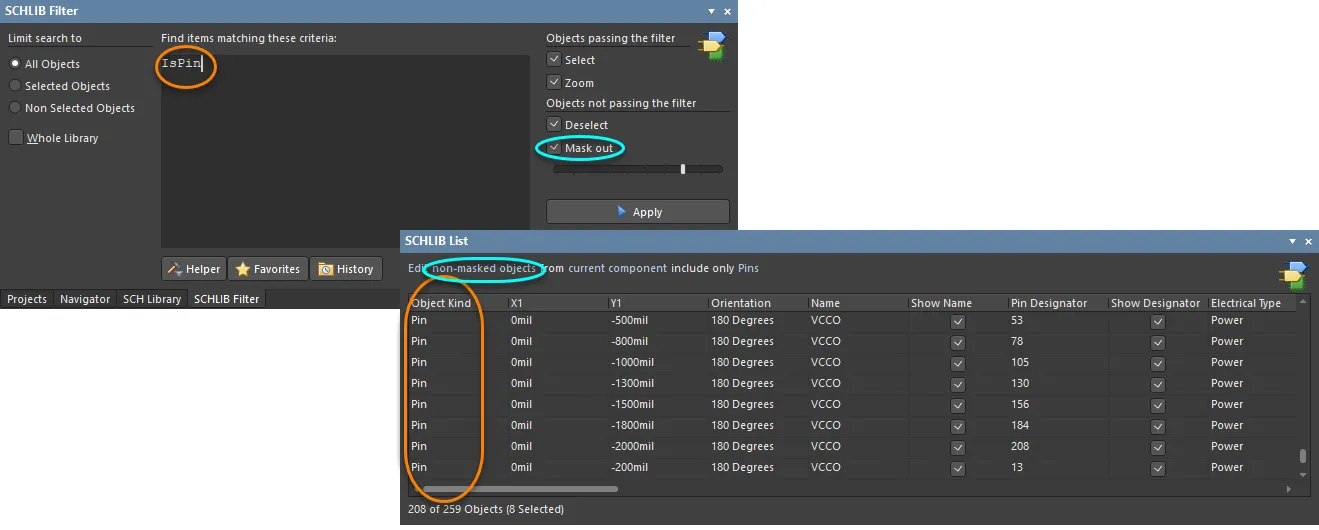
High-pin count and regularly sectioned components, such as FPGAs, lend themselves to implementation as multipart components in Altium NEXUS. The easiest way to do that is to create all the pins in the first part of the Altium NEXUS component, and then cut and paste the blocks of pins to the other parts.
To get the pins into neat, part-ready groups, try leaving a couple of empty rows between the pins for each part in the spreadsheet. Not only does it make it easy to see where you might need to restart coordinate values, you can also automatically add X, Y values to a large selection and then remove the redundant X, Y values in the empty rows. This will result in no pins in those deleted locations, neatly spacing the part-ready groups.

Use the tools in the spreadsheet to add suitable X and Y coordinates for the pins.
Select and copy the required cells in your spreadsheet. Don’t worry if there are columns in the selection that you don’t need, the Smart Grid tools can ignore these.
In Altium NEXUS, right-click in the SCHLIB List panel and select Smart Grid Insert from the menu to open the Smart Grid Insert dialog. If your source data includes a header row Altium NEXUS will attempt to automatically identify the object kind, then build a list of created objects. A point to keep in mind, before you map columns the list of created objects will have the properties of the current Altium NEXUS default pin object. So for example, if you wanted all the pins placed at 180 degrees with a length of 20, then set the default values in Altium NEXUS before starting the smart grid process. That way you don’t need to worry about adding those settings into the spreadsheet, or editing them in Altium NEXUS after the creation process. Not sure how to set the defaults? Just select Place » Pin from the menus, then before you place a pin press Tab to edit the default values, then place and delete that one pin.
Another big advantage of including a header row is that you get to use the Automatically Determine Paste button. This is a great feature – it will search and compare fields in the created object against source data column titles, and make intelligent choices about how they should be mapped. Don’t worry if the automatic feature gets one wrong, you can use the Undo Paste button to undo a mapped column. To manually map, select a column in the source data and its corresponding column in the created objects, then click the Paste Column button.
As soon as you click OK, the set of created objects will appear in the design space. Add a suitable body to each part, then cut and paste to create the individual parts, and your symbol is ready.

The Smart Grid Inserted pins, and the parts with the component bodies added.
Editing Attributes with Numeric Values
For a numerical-based attribute of an object, the simplest modification to that attribute's value is made by typing a new value to replace the existing one. The plus and minus operators can be used to specify the value's sign. A value entered without a specified sign is assumed to be positive. Therefore, entering 20 is the same as entering +20.
You can enter specific units of measurement for a value entered. The software will convert the value into the current units defined for the document. If no units are specified, the default units set for the document will be used.
Modification Using an Expression
More advanced modification can be achieved by using an arithmetic expression. Select the entry for the attribute you want to modify and type the expression that will be used to modify its value. You can enter any arithmetic expression using any built-in arithmetic operators and functions found in Pascal.
If you want to use the current value for the attribute as part of the expression, you will need to make reference to this original value either by using the full name of the attribute or by using the exclamation character (the supported substitute for the name of the attribute currently being modified). If you want, you may use any other attribute field name in an expression. When using attribute names, if any names contain spaces, they must be replaced by the underscore character.
To illustrate an example of using a simple expression, consider a component pin, the Length attribute of which is currently 30. If you wanted to extend this length to 45, you could enter the expression:
Length + 15
or, in shortened form:
! + 15
Note that the spaces are optional. When you press Enter, the value will be updated to 45.
If instead you want to shorten the pin to a length of 20, you could use the subtraction operator, as illustrated by the following expressions:
Length - 10

! - 10
To illustrate use of a function, the previous expression could be re-written as:
! - sqrt(100)
the result would be the same - a length of 20.
By using the attribute's name (or substitution character (!)) the previous expressions add to or subtract from the current value for the attribute. Without such entries in the expression, you would be setting the attribute's value to the evaluated result of the expression. For example, if the attribute name or substitution character had been left out of the previous expressions, the resulting pin length would have been 15 and -10.
Again, you can enter specific units of measurement for a value entered into an expression. The software will convert the value into the current units defined for the document. If no units are specified, the default units set for the document will be used.
By selecting multiple objects in the panel, you can change numerical attributes simultaneously using an expression. For example, you may want to adjust the length of a series of component pins or shift components vertically or horizontally by a specific distance.
Batch Replacement of String-based Attributes
There are times when you may want to modify a string-based attribute that is common to multiple selected objects in the workspace. For example, you may want to rename the display names of selected pin objects from D1, D2, D3, etc., to Data1, Data2, Data3, etc. To perform this type of batch replacement, the use of string substitution syntax is supported in the panel.
A string substitution entry is enclosed in braces and has the form:
{oldstring=newstring}
An entry of this form causes all occurrences of oldstring found in the attribute's value to be replaced with newstring. In the case of the pin display names, you would select the associated Name attribute cell for each pin, right-click then choose Edit (or press F2), then press Enter {D=Data} in the active value field.
If you want to replace multiple, differing string portions in the same target string, type multiple substitution entries each enclosed in its own set of curly braces. For example, consider the following display names associated with output pins of a component:
INTA

INTB

INTC

INTD
If the intended format for new display names is to be EXT_INT_x - where x represents 1, 2, 3, 4, then you could select the Name attribute for the four pins in the panel, switch to Edit mode then enter the following into the active value field:
{INT=EXT_INT}{A=_1}{B=_2}{C=_3}{D=_4}
The software takes this entry and effectively performs a batch substitution - substituting for the first expression, then the second, and so on.
Smart Editing of String-based Attributes

The SCHLIB List panel offers further support for string modification through its Smart Edit feature. Select the cell entries pertaining to the attribute that you want to modify for all required objects, right-click then choose Smart Edit from the menu. The Smart Edit dialog will open.
The Smart Edit dialog offers two methods for performing string modification accessed from the Batch Replace and Formula tabs.
Batch Replace Tab
The Batch Replace tab provides straightforward substitution, along the lines of the string substitution discussed previously (without having to enter the curly braces). Click inside the From field then enter the portion of the current string that you want to replace. Click inside the To field then enter the string to be used as the replacement. The familiar string substitution syntax is displayed at the bottom of the tab.
For example, consider pins of a component that have the prefix D as part of their display Name and you need to change them to have a prefix of DATA instead. In this case, select the Name attribute for each of the pins in the panel then access the dialog. On the Batch Replace tab, enter D in the From field and DATA in the To field (the replacement string is therefore {D=DATA}). After clicking OK, the display Name will be modified accordingly.
As with basic string substitution, the Batch Replace tab provides for replacement of multiple, differing string portions in the same target string. Enter the various substitutions as distinct From-To entries. Consider the previous INTx example (see Batch Replacement of String-based Attributes), where strings of the form INTx (x = A, B, C, D) need to be changed to EXT_INT_x (x = 1, 2, 3, 4). In this case, you would enter four distinct substitution entries on the Batch Replace tab.
Formula Tab
The Formula tab provides for more advanced modification, allowing you to apply a specific expression to the selected string objects. The expression can include any built-in arithmetic operators and functions that apply to strings (found in Pascal). If you want to use the current value for the attribute as part of the expression, you will need to make reference to this original value, either by using the full name of the attribute or by using the exclamation character (the supported substitute for the name of the attribute currently being modified). When using attribute names, if any names contain spaces, these must be replaced by the underscore character. For example, use of the Pin Designator field within a formula should be entered as Pin_Designator.
Consider, for example, three pins specified for a schematic component with designators 1, 2, and 3. You might want to extend the designators of these pins by including some indication of their role. First, select the cell entries for the Pin Designator attributes of these pins. Then, using the addition operator, you could write an expression to add to the existing string value of the Pin Designator attribute. This would take the existing (original) string value and concatenate it with a specified new string as illustrated below:
'ADDR_' + Pin_Designator
or, in shortened form:
'ADDR_' + !
Note that the spaces are optional. After clicking OK, the designators of the pins will be updated to ADDR_1, ADDR_2, and ADDR_3.
To illustrate the use of string-based functions, consider the Copy function that can be used to take a portion of an original string and replace it within an expression to create a new string. For example, pin display names of the format DATA_I_x[7..0] now need to be changed to the format EXT_DAT_I_x[31..0]. In this case, you could select the cell entries for each pin's Name attribute, access the Smart Edit dialog and write the following expression on the Formula tab:
'EXT_' + Copy(Name,1,3) + 'I' + Copy(Name,7,3) + '31..0]'
or, in shortened form:
'EXT_' + Copy(!,1,3) + 'I' + Copy(!,7,3) + '31..0]'
Right-click Menu
The right-click menu for the main list area of the panel provides the following commands:
- Switch to View/Edit Mode - click to toggle between View and Edit mode.
- Edit - allows you to edit single or multiple selected objects with respect to a particular attribute in the list. When editing a single object, the command becomes available when an attribute cell entry for a design object is editable. After launching the command, you will be able to edit the value in the selected cell directly. Click outside the cell or press Enter to effect the change. When simultaneously editing multiple objects, the command will become available only if the chosen attribute is editable for all objects in the selection. After launching the command, you will be able to edit the value in the focused cell directly. Click outside the cell or press Enter to effect the change across all cells in the selection.
- Smart Edit - click to open the Smart Edit dialog in which you can specify the criteria used to perform batch replacement of string-based attributes.
- Copy - click to copy the selected cells in the list to the Windows clipboard for use in other applications.
- Copy with Header - copy tabular data including the header row.
- Paste - click to paste the current content of the Windows clipboard into the list. Combined with the Copy command, this enables you to copy cell content out to another spreadsheet application, make modifications then paste the modified data back into the SCHLIB List panel.
- Smart Grid Paste - click to open the Smart Grid Paste dialog to change the value of existing objects from pasted tabular data. The SCHLIB List panel must be in Edit mode to access this command.
- Smart Grid Insert - click to open the Smart Grid Insert dialog to create new objects from the tabular data. TheSCHLIB List panel must be in Edit mode to access this command.
- Show Children - used to add object entries to the list with respect to the primitives that constitute group objects (e.g., Parts).
- Zoom Selected - zooms and centers (where possible) the selected objects in the design editor window.
- Report - use to generate a report containing all objects displayed in the list. After launching the command, the Report Preview dialog opens in which you can view, print and export the report in various file formats. The report will contain only data that is visible in the panel.
- Report Selected - use to generate a report containing only those objects that are currently selected in the list. After launching the command, the Report Preview dialog will open in which you can view, print and export the report in various file formats. The report will contain only data that is visible in the panel.
- Select All - use to select all objects in the list. The corresponding design objects will become selected in the main design workspace.
- Select Column(s) - use to select all cells in the column associated with the currently selected cell. All corresponding objects will become selected in the design workspace. This command is particularly useful when editing a particular attribute of multiple objects.
- Select Row(s) - use to select all cells in the row associated with the currently selected cell. All corresponding objects will become selected in the design workspace. This command is particularly useful when editing a particular attribute of multiple objects.
- Choose Columns - use to access the Columns Setup dialog in which you can determine the available attribute columns that are displayed in the panel and the order in which the columns appear. By default, the Display Mode for each attribute will be set to Automatic. In this mode, an attribute column will be automatically displayed if it is common to all design objects currently displayed in the panel. Click on the mode for pop-up options that allow you to force the display of the attribute or to hide it completely.

List Shortcuts
The following table summarizes key shortcuts that are available when using the main list region of the panel.
|
Arrow Keys
|
Shift focus to next cell in direction of arrow key
|
|
Left-Click & Drag
|
Multi-select in direction of mouse movement
|
|
Ctrl + Click
|
Multi-select (non-sequential)
|
|
Shift + Click
|
Multi-select (sequential)
|
|
Spacebar or F2
|
Edit selected cell
|
|
Enter
|
Finish editing current cell and enter edit mode for cell beneath
|
|
Ctrl + C (or Ctrl + Insert)
|
Copy
|
|
Ctrl + V (or Shift + Insert)
|
Paste
|
|
Page Up
|
Jump selection to top of visible list area
|
|
Page Down
|
Jump selection to bottom of visible list area
|
|
Mouse-wheel
|
Pan up or down
|
Tips
- Press Shift + F12 to toggle the visibility of the panel in the workspace.
- When any filtering currently applied to the workspace is cleared, the option to display non-masked objects in the panel will produce the same result as choosing the option to display all objects.
