The schematic symbol typically includes a shape that can reflect the function of the component and one or more pins. How a component is represented, i.e. the look of the symbol and arrangement of component pins, is up to the designer. This should be done to comply with the requirements of your organization and the design standards you choose to adopt. One component symbol can represent the entire physical component, or the component can be defined by multiple sub-parts where each sub-part represents some logical entity within the physical component (e.g., each AND gate in a quad AND gate component, or the coil and contact sets in a relay). This type of component is also called a multi-part component.
Creating a New Schematic Symbol
Schematic symbols can be created directly in your connected Workspace:
-
Select File » New » Library from the main menus, then in the New Library dialog that opens, select Create Library Content » Symbol from the Workspace region of the dialog.

Create a new Workspace Symbol using the New Library dialog
-
In the Create New Item dialog that opens, enter the required information, make sure that the Open for editing after creation option is enabled and click OK. The Workspace Symbol will be created, and the temporary schematic symbol editor will open, presenting a .SchLib document as the active document. This document will be named according to the Item-Revision, in the format: <Item><Revision>.SchLib (e.g., SYM-001-0001-1.SchLib). Use the document to define the symbol as described below.

Example of editing the initial revision of a Workspace Symbol – the temporary schematic symbol editor provides the document with which to define your schematic symbol.
-
When the symbol is defined as required, save it to the Workspace using the Save to Server control to the right of the symbol's entry within the Projects panel. The Edit Revision dialog will appear, in which you can change Name, Description, and add release notes as required. The document and editor will close after saving.
A saved Workspace Symbol can be used when defining a component using the Component Editor in its Single Component Editing mode or Batch Component Editing mode.
Workspace Symbols can be browsed using the Components panel. Enable visibility of models by clicking the  button at the top of the panel and selecting Models, then select the Symbols category.
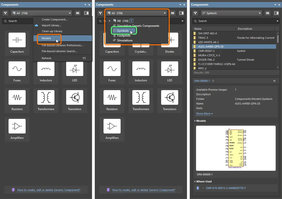
To edit a Workspace Symbol, right-click its entry in the Components panel and select the Edit command. Once again, the temporary editor will open, with the symbol opened for editing. Make changes as required, then save the document into the next revision of the Workspace Symbol.
When saving an edited symbol to your Workspace, you can preserve the symbol's current lifecycle state. Control is provided courtesy of the Preserve lifecycle state (not recommended) option available in the Create Revision dialog when re-saving ( ). When the option is enabled, the new symbol revision will automatically be set to the lifecycle state of the previous revision. This ability is available for those with assigned Allow to skip lifecycle state change for new revisions operational permission (learn more about Setting Global Operation Permissions for a Workspace).
Updating Related Component
When you make a change to a Workspace domain model – be it a symbol, footprint model, or simulation model – the moment you save that change into a new revision of the model, any Workspace Components that use that model will become effectively out of date, still using the previous revision. In most cases, you will no doubt want to re-save those Workspace Components, with the respective model links updated to use the latest revisions available. To streamline this process, a Workspace, in conjunction with Altium Designer, facilitates the ability to update related components – at the point of re-saving a Workspace model – after having made any modifications to that model through the direct editing feature.
The option to perform this update to the parent components can be found in the Create Revision dialog that appears when saving the modified Workspace Symbol back to the target Workspace. This option – Update items related to <ModelItemRevision> – is enabled by default.
<ModelItemRevision> is the current revision of the model, that is, the revision currently being used by any related Workspace Components. Once the Workspace model itself is saved, this would naturally be the previous (earlier) revision, and no longer the latest.

Accessing the option to update related Workspace Components that are referencing the Workspace Symbol being re-saved.
If you want to keep all related components using the current revision of the Workspace Symbol, disable this option. Only the Workspace model itself will then be saved.
Once you click OK in the Create Revision dialog, the modified symbol is saved back to the Workspace, and its associated temporary editor is closed. All Workspace Components referencing that Workspace Symbol will be re-saved to use its new revision automatically (the next revision of each component is automatically created and the save performed).
-
From a designer's perspective, a Workspace Component gathers together all information needed to represent that component across all design domains, within a single entity. It could therefore be thought of as a container in this respect – a 'bucket' into which all domain models and parametric information are stored. In terms of its representation in the various domains, a Workspace Component doesn't contain the Workspace domain models themselves, but rather links to these models. These links are specified when defining the component.
-
Schematic symbols can also be created in the Workspace as part of importing existing, older generation (SchLib, PcbLib, IntLib, DbLib, SVNDbLib) libraries of components. The interface to this process – the Library Importer – presents an intuitive flow that takes initial selected libraries, and imports them to your Workspace. Learn more about the Library Importer.
-
A new Workspace Symbol can also be created when defining a Workspace Component in the Component Editor in its Single Component Editing mode.
-
A symbol can also be created as part of a file-based schematic symbol library.
Defining a Schematic Symbol
Schematic symbols are created by placing drawing objects to represent the component body and pins that represent the physical pins on the actual component. Schematic symbols are created in Altium Designer's schematic symbol editor.
Notes about symbol creation:
-
Objects placed in the library editor are stacked in the order they are placed. Use the Edit » Move commands to change the display order if the pins become hidden behind the component body.
-
Only one end of a pin is electrical. This end is referred to as the hotspot. Make sure the hotspot (the end by which you hold the pin) is away from the component body. Refer to the Pin object for more information.
-
In the schematic library editor, the properties of the currently active symbol, such as the default designator and the description, are edited in the Properties panel in Symbol mode. The panel displays in this mode when nothing is selected. If you double-click on a primitive placed as part of the component symbol, the Properties panel will display the properties of that primitive rather than the parent component.
-
The option used to display the designator and comment on the symbol editor sheet (Show Comment/Designator) is enabled/disabled for the current library in the Library Options mode of the Properties panel. Select the Tools » Document Options command to display the Properties panel in this mode.
-
The fonts can be configured individually for each object as they are placed, or you can set your preferred fonts for new objects by editing each of the appropriate objects on the Schematic - Defaults page of the Preferences dialog.
-
Use the Schematic Symbol Generation Tool to quickly build high-pin count components. The tool also supports importing pin details from a spreadsheet via the right-click menu.
-
Multiple pins can be imported from a spreadsheet into the current symbol via the Smart Grid commands on the right-click menu in the SCHLIB List panel – learn more.
When creating a Workspace Symbol, note that only the symbol graphics need to be defined – the representation of the higher-level component within the schematic editing domain. It is not a 'schematic component' as defined for use in older file-based component management methodologies, where other models and parameters are defined as part of that schematic component. A component needs only the graphical depiction of the symbol. It will include links to other domain models and parameters as part of its own definition.
Before you start creating component symbols, it is worth spending some time configuring your preferred defaults. The defaults for all schematic design objects (both library and sheet) are configured on the Schematic - Defaults page of the Preferences dialog. When the Preferences dialog page is open, press F1 for more information about an option.
Preparing the Design Space
Always draw the component symbol close to the sheet origin (the center of the sheet). If necessary, relocate the origin of the sheet to the center of the design window by selecting Edit » Jump » Origin (shortcut J, O). Check the Status bar at the bottom left of the screen to confirm that you have the cursor at the origin. Components supplied by Altium are created around this point, marked with a crosshair through the center of the sheet. You should always create your components close to this origin.
When you place a component on the schematic, the component is 'held' by the sheet origin of the library symbol. A common approach used when creating the symbol is to place the hotspot of pin 1 of the component at the sheet origin, resulting in it being held by that pin during placement from the library onto the schematic sheet. While this is not mandatory (you are free to place the symbol pins and body objects anywhere on the sheet), if you place the symbol objects away from the origin, then the component will be the same distance away from the cursor when you place it from the library onto a schematic sheet.
The default units for schematic and schematic library grids are imperial. Since all Altium components are designed on this imperial grid, it is important to appreciate the impact of deciding to switch to a metric sheet grid as it becomes difficult to correctly wire to components created on different grids. Note that imperial grids can be used with metric sheet sizes, such as A3, so it is not necessary to change to a metric grid when working with metric-sized sheets. The units for the current sheet are defined on the General tab in the General region of the Properties panel in Library Options mode (use the Tools » Document Options command from the main menus to access this mode of the Properties panel).

Use the General region of the Properties panel in Library Options mode to set the units for the current sheet.
Units for new sheets (schematic and library) are defined on the
Schematic – General page of the
Preferences dialog.
If desired, enable the Show Comment/Designator option in the Properties panel to display the Comment/Designator strings for the current component in your library document.
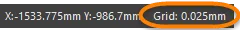
Objects are placed on the current snap grid. The current grid is displayed at the bottom of the design space on the left-hand end of the Status bar.
The Snap Grid and Visible Grid can also be set in the Properties panel in Library Options mode. Rather than opening the Properties panel whenever you need to change the grid, you can press G to cycle the snap grid through the available settings. Available settings can be edited on the Schematic – Grids page of the Preferences dialog.
Typically, objects and pins are placed on a grid of 100 mil or 50 mil, with strings being the only object needing to be placed on a grid of 10 mil. To assist during the positioning of text strings, press Ctrl as you move a string to temporarily switch the grid to the finest setting (the default is 10 mil).
Properties Panel
When the active document is a Schematic Library document (*.SchLib), choose the Tools » Document Options command from the main menus – the Properties panel presents the Library Options. The following collapsible sections contain information about the options and controls available:
Selection Filter
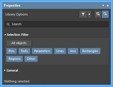
The options in this section of the panel determine which schematic library objects may be selected in the design space.
-
All Objects button – select remove object filtering so that all types of objects may be selected.
-
Object buttons – toggle each object button to enable/disable the ability to select that object type.
General
When a design object is selected, the panel will present options specific to that object type. The following table lists the object types available for placement within the library design space. Click a link to access the properties page for that object.
Creating the Schematic Symbol Body
After setting up the design space options as required, the next step is to capture the graphical representation of the component, i.e. to create the symbol graphics that will represent that component when placed on a schematic sheet. It is important to decide upon a standard for the graphical schematic symbols by which to adhere. This will provide a formal template when designing the symbol graphics and result in a guaranteed level of consistency. Altium's design methodology follows standard IEEE 315, which not only covers the most common circuit elements but also clearly defines how semiconductor elements can be combined to symbolize any number of silicon device types.
The body of the symbol is created by placing graphical design objects in the schematic library editor design space by using the Place menu, the Utilities bar, or the Active Bar. Double-click the placed schematic symbol to open the Properties panel to further define each shape.
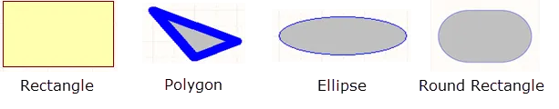
Altium Designer includes a variety of closed symbol shapes including rectangle, polygon, ellipse, and round rectangle as shown below.
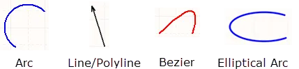
Line-type shapes include arc, line/polyline, bezier, and elliptical arc. Lines/polylines can include arrowheads and tails. Double-click to open the Properties panel to define the heads and tails.
Adding Pins to the Symbol
It is the component pins that give the component its electrical properties and define connection points on the component for directing signals in and out. A pin is placed to represent each pin on the actual physical component.
A pin can be added to the component that is currently visible in the schematic library document design space using one of the following methods. In each case, the pin appears floating on the cursor held by the electrical end. Rotate and/or flip the pin as required and click to effect placement.
-
Use the Place » Pin command (or shortcut P, P).
-
Click the  button on the Active Bar.
-
Click the button on the design object drop-down of the Utilities toolbar.
-
Using the Component Pin Editor dialog – when no object is selected in the design space, the Properties panel can be used to edit the properties of the symbol, including editing, adding, or deleting pins. The panel also gives access to the Component Pin Editor dialog; to open it, click the  button on the Pins tab of the Properties panel. The dialog provides a single, convenient location for you to modify certain properties of any pin associated with the symbol. In addition to providing a means of editing pin properties, the dialog also allows you to add new pins or delete existing ones.
 Access the Component Pin Editor dialog with which to manage all of the pins for your created symbol.
Options and Controls of the Component Pin Editor Dialog
Pin Grid
This area presents all pins for the component. For each pin, the following information is displayed:
-
Designator – the numerical identifier of the pin. Each pin of a part must have a unique designator.
-
Name – the display name for the pin. Note that the name is optional, this field can be left blank if required. Alternatively, enter a string into the Name text field, then use the Name checkbox to display or hide the name.
-
Desc – the description of the pin.
-
Footprint Model Mapping – the pad of the indicated linked footprint model to which this pin of the schematic component is mapped. A separate column is presented for each linked footprint model.
The mapping of component pins to model pins can be updated in the Model Map dialog.
-
Type – the electrical type of the pin. This type is used when compiling a project or analyzing a schematic document to detect electrical connection errors (using the Electrical Rules Check feature). Available types are Input, I/O, Output, Open Collector, Passive, HiZ, Open Emitter, and Power.
-
Owner – the parent part to which the pin is associated. For a single-part component, this entry will always be 1; it is only meaningful for a multi-part component. A multi-part component also includes a non-graphical part, Part Zero. Part Zero is used for pins that are to be included in all parts of the multi-part component, for example, power pins.
-
For a multi-part component, the power net connections should ideally be assigned through the use of Part Zero. A pin is included in Part Zero by placing it, then setting the Part Number property to
0. Pins placed in Part Zero will appear on all parts.
-
The pins placed in Part Zero can also be hidden if required. While this practice is not recommended, for each pin that is required to connect to a power net in this way, enter the net name in the Hidden Net Name field in either the SCHLIB List panel or the SCH List panel and then disable the Show option in the Component Pin Editor dialog (or enable the Hide option in the SCHLIB List panel or the SCH List panel).
-
Show – reflects whether the pin is visible on the sheet (enabled) or hidden (disabled). While this practice is not recommended, the power pins of multi-part components can be hidden when their display would otherwise cause unnecessary clutter on the schematic sheet.
Hidden pins for a component can be revealed on the sheet in the schematic editor or schematic library editor by enabling the Show All Pins option in the Pins region of the Properties panel. In the schematic library editor, the Show Hidden Pins option must also be enabled in the Edit main menu.
-
Number – used to determine whether the designator for the pin is displayed (enabled) or hidden (disabled) when the parent part is placed on a schematic sheet.
-
Name – used to determine whether the display name for the pin is displayed (enabled) or hidden (disabled) when the parent part is placed on a schematic sheet.
To negate (include a bar over the top of) a pin name, use one of the following methods:
-
Include a backslash character after each character in the pin name (e.g.
H\O\L\D\).
-
Enable the Single '\' Negation option on the Schematic – Graphical Editing page of the Preferences dialog, then include one backslash character at the start of the pin name (e.g.
\HOLD).
-
Pin/Pkg Length – this is the pin-package length.
-
Propagation Delay – displays the propagation delay, which is the amount of time it takes for the head of the signal to travel from the sender to the receiver.
-
Add – click this button to add a new pin to the component. The new pin will be assigned the next available designator (which can be pin 0), and will have the following default properties:
-
Name –
1
-
Desc – blank
-
Mapping – all
0
-
Type –
Passive
-
Owner – the number of the active/selected part.
-
Show/Number/Name – all enabled.
Upon clicking OK in the dialog, any newly added pins will be initially placed at the bottom-right of the component (or part thereof). Reposition as required.
-
Remove – click this button to remove the currently selected pin from the component. A confirmation dialog will open; click Yes to proceed with the removal. If removing a pin from a placed component instance on a schematic, you may need to rewire any existing wiring that was connected to that pin.
The following tips relate to working with the Pin Grid:
-
With the exception of fields displaying mapping information for any models linked to the parent part, all fields are editable. Click once on a field to select it then type the value or select the option as required. Click away from the field or press Enter to make the change.
-
For a multi-part component, the pins for the active/selected part will be presented with a normal white background, with the pins of all other parts presented with a grey background.
-
Pins can be sorted by various fields using the column header in each case. Click once to sort in ascending order, click again to sort in descending order. Shift+Click to sort by additional fields. Ctrl+Click to remove sorting.
Right-Click Menu
The grid right-click menu offers the following commands:
-
Jump – use to jump to the currently selected pin within the design space (zoomed and centered (where possible)).
-
Add – use to add a new pin to the component (or part thereof).
-
Remove – use to remove the currently selected pin from the component. A confirmation dialog will open; click Yes to proceed with the removal.
-
Edit – this command is non-functional.
-
Report – use to open the Report Preview dialog.
Properties Region
General Tab
-
Font Settings
-
Designator
-
Custom Settings – enable to access the Font Settings below to customize the font.
-
Font Settings – use the controls to configure the font, font size, color, and special settings such as bold and underlining.
-
Custom Position – enable to access the controls below to customize the position.
-
Margin (X/Y) – enter the desired margins.
-
Orientation – use the drop-down to select the orientation.
-
To – use the drop-down to select the desired object of the designator.
-
Name
-
Custom Settings – enable to access the Font Settings below to customize the font.
-
Font Settings – use the controls to configure the font, font size, color, and special settings such as bold and underlining.
-
Custom Position – enable to access the controls below to customize the position.
-
Margin (X/Y) – enter the desired margins.
-
Orientation – use the drop-down to select the orientation.
-
To – use the drop-down to select the desired object of the name.
Parameters Tab
-
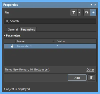
Parameters – this region lists all of the parameters currently defined for the pin. Use the
 or
or  icon to show/hide the value of the associated parameter in the design space. Use the
  or
or  icon to lock/unlock the associated parameter.
-
Name – the name of the parameter. For a rule-type parameter, this entry will be locked as
Rule.
-
Value – the value of the parameter. For a rule-type parameter, the entry will reflect the rule type along with a listing of its defined constraints.
-
Font – click to open a menu to select the desired font, font size, color, and attributes to bold, italicize, etc., if desired.
-
Other – click to open a drop-down to change additional options:
-
Show Parameter Name – enable to show the parameter name.
-
Allow Synchronization with Database – enable to synchronize with the database.
-
X/Y – enter the X and Y coordinates.
-
Rotation – use the drop-down to select the rotation.
-
Autoposition – check to enable auto-positioning.
-
Add – click to add a parameter. Use
 to delete the currently selected parameter.
For a
multi-part component, the relevant pins for the selected part will be highlighted in the
Component Pin Editor dialog. All pins of other parts are grayed out.
The Component Pin Editor dialog can also be accessed in the Schematic Editor, for a placed component (or part thereof).
Configuring Pin Properties
Press Tab to open the Component mode of the Properties panel to edit the pin properties before placement. Numerical values will auto-increment on subsequent pin placements. Auto-increment behavior is configured in the Auto-Increment During Placement settings on the Schematic – General page of the Preferences dialog. Use negative values to auto-decrement.

Use the Schematic - General page of the Preferences dialog to define auto-increment behavior. During placement or whenever a pin is moved, the pin is held by the electrical end (also called the hot end of the pin). The pin must be positioned so that the electrical end is away from the component body. Press the spacebar to rotate a pin while it is being moved.
Pins also can be placed to represent electro-mechanical points on the component, such as the tab on a voltage regulator.
A pin has a number of properties including a Name and a Designator. It is the pin Designator that is used to match the symbol pin to the PCB footprint pad. The default distance that the pin's Designator and Name appear from the end of the pin is a system-wide setting for the Schematic and Schematic Library editor. Configure the Pin Margin on the Schematic – General page of the Preferences dialog.
Individual settings for the Name can be configured in the Component Pin Editor dialog.
A pin has an Electrical Type that is used by Altium's electrical rules check system to verify that pin-to-pin connections are valid. Set this option in the Component Pin Editor dialog to suit the electrical type of that component pin. The default Pin Length should suit the chosen snap grid (typically 100 mil or 50 mil). The default length is 30; typical lengths are 20 or 30.
Symbols can be added in the Component Pin Editor dialog to different positions of the Pin to represent electrical information from the pin.
Pin

The schematic Pin represents the physical component pin in the schematic design space.
Summary
A pin is an electrical design primitive. Pins give a component (part) its electrical properties and define the connection points on the part for the incoming and outgoing signals.
Availability
Pins can only be placed in the schematic library editor using one of the following methods:
-
Click Place » Pin from the main menus.
-
Click
 on the drop-down of the Utilities toolbar (
 ).
).
-
Right-click then choose Place » Pin from the context menu.
Placement
After launching the command, the cursor will change to a cross-hair and you will enter pin placement mode. Placement is made by performing the following sequence of actions:
-
Click or press Enter to anchor the pin. Note that the floating pin is held by the electrical end, which must be positioned away from the component body. Only one end of the pin is electrical; it is always this end that the pin is held.
-
Continue placing additional pins or right-click or press Esc to exit placement mode.
Additional actions that can be performed during placement – while the pin is still floating on the cursor, and before the electrical end of the pin is anchored – are:
-
Press the Tab key to pause the placement and access the Pin mode of the Properties panel from where its properties can be changed on the fly. Click the design space pause button overlay (
 ) to resume placement.
-
Press the Alt key to constrain the direction of movement to the horizontal or vertical axis depending on the initial direction of movement.
-
Press the Spacebar to rotate the pin counterclockwise or Shift+Spacebar for clockwise rotation. Rotation is in increments of 90°.
-
Press the X or Y keys to mirror the pin along the X-axis or Y-axis.
Create the Library component near the origin (center) of the Library Editor sheet, which is marked by dark cross-hair lines. Typically a pin or the corner of the component body is placed at the sheet origin.
The pin number (Designator) must be defined since that is what is used to establish the connectivity. The Electrical Type is also important as this is used in the Schematic Editor for the Electrical Rules Check (ERC).
Notes on Pin Numbering
For many components, there will be a series of pins that have numerical names and numbers. The Auto-Increment During Placement feature on the Schematic – General page of the Preferences dialog can be used to speed the placement of these pins. Auto-increment is invoked automatically if the pin properties are edited before placement (press Tab while the pin is floating on the cursor). The feature works for both the Designator and the Name; the pin Designator uses the Primary auto-increment field and the pin Name uses the Secondary auto-increment field. It supports ascending alpha and numeric values and descending numeric values.

Configure the Auto-Increment During Placement settings on the Schematic – General page of the Preferences dialog.

Note the increasing alpha pin name and decreasing numeric pin number.
Graphical Editing
To move a pin, click and hold. The cursor will jump to the electrical hotspot end of the pin; move it to the new location, placing it with the electrical end away from the component body.
While dragging, the pin can be rotated (Spacebar/Shift+Spacebar) or mirrored (X or Y keys to mirror along the X-axis or Y-axis).
Non-Graphical Editing
Editing via the Pin Dialog or Properties Panel
Properties page: Pin Properties
The properties of a Pin can be edited in the Pin dialog and the Properties panel, which allows editing of all item(s) currently selected in the design space.
Pin Display Name and Designator – Position and Font
The location of the pin name and designator is defined globally in the Pin Settings region on the Schematic – General page of the Preferences dialog. This is an environment setting, meaning it applies to the PC where the setting is defined. The settings define a relative distance (margin) the text is away from the non-electrical end of the pin.
 in the Preferences dialog.")
Set the distance of the pin text (Pin Settings) in the Preferences dialog.
The default system font for a schematic library document is Times New Roman, 10pt, Regular. This is fixed and cannot be changed. When a library component is placed on a schematic sheet, this same default font is applied but is not fixed and can be changed as required. Keep in mind that the system font used for a schematic sheet applies to other objects as well, including power ports, ports, and the X, Y region markers in the schematic sheet border.
For pins, the system-level settings of position, margin and font can be overridden. Controls for customization of the pin's Designator and Name can be found in the Properties panel in the Font Settings region.

The Font Settings of the pin Designator and Name can be modified for individual pins if required.
Use the Custom Position option to change the default settings for the position to an overriding, customized position. For the Margin (X/Y), enter a new value directly in the associated field for X and Y. For the Orientation, use the drop-down to choose the angle and the To reference.
Use the Custom Settings option to change from using the default system font to using an overriding, customized font.
Pin Symbol Line Width
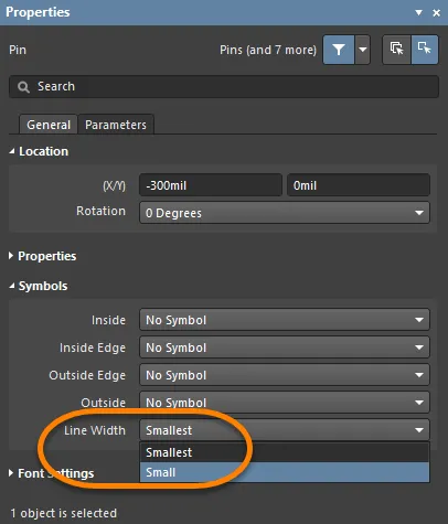
When representing a component in the schematic editing domain, each pin defined as part of that device's schematic symbol can have one or more symbols displayed. These are symbols displayed on the Inside, Inside Edge, Outside, or Outside Edge in relation to the main component symbol outline, as required. Examples might include a Clock symbol on the Inside Edge or a Dot symbol on the Outside Edge. Such symbols greatly improve the readability of the design through visual indication of the purpose of the signal traversing a particular pin.
Use the Line Width setting in the Symbols region of the Properties panel to specify the width of the line used to draw these symbols. Choose from either Small or Smallest.
Older designs sometimes included components with hidden power pins, which were connected to the appropriate power net. While this practice is not recommended, hidden pins can be connected by entering the net name in the Hidden Net Name field in the SCHLIB List or SCH List panels.
Pin Properties

General Tab
Location
-
(X/Y)
-
X (first field) – the current X (horizontal) coordinate of the reference point of the object, relative to the current design space origin. Edit to change the X position of the object. The value can be entered in either metric or imperial; include the units when entering a value whose units are not the current default.
-
Y (second field) – The current Y (vertical) coordinate of the reference point of the object, relative to the current origin. Edit to change the Y position of the object. The value can be entered in either metric or imperial; include the units when entering a value whose units are not the current default.
-
Rotation – use the drop-down to select the rotation.
Properties
-
Designator – the numerical identifier of the pin. Each pin in a part must have a unique designator. Use
 or
or  to determine whether the Designator for the pin is displayed or hidden (respectively) when the parent part is placed on a schematic sheet.
-
Name – use to specify an optional display name for the pin. By default, a newly placed pin will be named using the designator value. Supplying a display name is particularly useful for IC-type components where a meaningful name enables you to see quickly how the pin is being used. Use or to determine whether the Name for the pin is displayed or hidden when the parent part is placed on a schematic sheet.
To negate (include a bar over the top of) a pin name, use one of the following methods:
-
Include a backslash character after each character in the pin name (e.g.
H\O\L\D\).
-
Enable the Single '\' Negation option on the Schematic – Graphical Editing page of the Preferences dialog, then include one backslash character at the start of the pin name (e.g.
\HOLD).
-
Function – use this field to specify a number of names (functions) for the multi-functional pin being edited. Enter an alternative name of the pin, then press Enter or click the  button at the right of the field. Added alternative names will be shown as labels below the field. Click '
x' in the label of a function to remove it.
-
There are no limitations for the field, and numbers and/or special characters (&, *, %, etc.,) can be used.
-
All Font Settings for the custom name are the same as the original pin name.
-
After placing the component on a schematic sheet, the function that will be shown as the pin name can be selected on the Pins tabs of the Properties panel in the Component mode.
-
Electrical Type – use the drop-down to set the electrical type of the pin. This is used when compiling a project or analyzing a schematic document to detect electrical connection errors (using the Electrical Rules Check feature).
-
Description – enter a meaningful description of the pin, if desired.
-
Pin Package Length – enter the pin-package length. The unit will automatically be entered after you press Enter.
-
Propagation Delay – this field lists the propagation delay, which is the amount of time it takes for the head of the signal to travel from the sender to the receiver.
-
Part Number – this field is available when the pin is being added to a multi-part component. Use the up/down arrows to specify the part to which the pin is to be associated. A multi-part component also includes a non-graphical part, Part Zero. Part Zero is used for pins that are to be included in all parts of the multi-part component, for example, power pins.
-
Pin Length – use to specify the length of the pin in accordance with the currently defined units of measurement. Click the color box to edit the color of the pin.
Symbols
These symbols are purely graphical. The true electrical property of the pin is determined by the entry set for the pin's Electrical Type.
-
Inside – use to optionally add a symbol to the pin on the inside of the component graphic.
-
Inside Edge – use to optionally add a symbol to the pin on the inside edge of the component graphic.
-
Outside Edge – use to optionally add a symbol to the pin on the outside edge of the component graphic.
-
Outside – use to optionally add a symbol to the pin on the outside of the component graphic.
-
Line Width – use this field to determine the width of the line used to draw the symbols. This provides support for meeting GOST standards, which stipulates that these symbols should be of the same width as the line used to draw the component's symbol.
The Line Width setting will also apply to the automatic symbol used in relation to the pin's defined Electrical Type.
Font Settings
-
Designator
-
Custom Settings – enable to access the Font Settings below to customize the font.
-
Font Settings – use the controls to configure the font, font size, color, and special settings such as bold and underlining.
-
Custom Position – enable to access the controls below to customize the position.
-
Margin (X/Y) – enter the desired margins.
-
Orientation – use the drop-down to select the orientation.
-
To – use the drop-down to select the desired object of the designator.
-
Name
-
Custom Settings – enable to access the Font Settings below to customize the font.
-
Font Settings – use the controls to configure the font, font size, color, and special settings such as bold and underlining.
-
Custom Position – enable to access the controls below to customize the position.
-
Margin (X/Y) – enter the desired margins.
-
Orientation – use the drop-down to select the orientation.
-
To – use the drop-down to select the desired object of the name.
Parameters Tab
Parameters
Use this region to manage parameters attached to the currently selected pin object.
-
Grid – this region lists all of the parameters currently defined for the pin. Use the or
 icon to show/hide the value of the associated parameter in the design space. Use the
  or icon to lock/unlock the associated parameter.
-
Name – the name of the parameter. For a rule-type parameter, this entry will be locked as
Rule.
-
Value – the value of the parameter. For a rule-type parameter, the entry will reflect the rule type along with a listing of its defined constraints.
-
Font – click to open a menu to select the desired font, font size, color, and attributes to bold, italicize, etc., if desired.
-
Other – click to open a drop-down to change additional options:
-
Show Parameter Name – enable to show the parameter name within the Schematic Library editor.
-
Allow Synchronization with Database – enable to synchronize with the database. This option is used to control if the comment can be updated. By default, these options are enabled to always allow synchronization with the source library/database. You may disable this option to prevent that comment from being included in an update process.
-
X/Y – enter the X and Y coordinates desired.
-
Rotation – use the drop-down to select the rotation.
-
Autoposition – check to enable auto-positioning, meaning that the text will remain in the chosen position as the component is moved and rotated.
-
Add – click to add a parameter. Use to delete the currently selected parameter.
Older designs sometimes included components with hidden power pins, which were connected to the appropriate power net. While this practice is not recommended, hidden pins can be connected by entering the net name in the Hidden Net Name field in the SCHLIB List or SCH List panels.
Pasting Array
In addition to the standard cut, copy and paste commands, you can also use the Edit » Paste Array command from the main menus when creating a component symbol to place the current clipboard contents onto the current document, as a vertical or horizontal object array. This can be particularly useful when the component symbol being created should include multiple pins.
After launching the command, the Setup Paste Array dialog will appear.

The Setup Paste Array dialog
Options and Controls of the Setup Paste Array Dialog
Placement Variables
-
Item Count - use this field to specify the total number of duplicate items to be pasted into the workspace.
-
Primary Increment - use this field to specify the amount to increment by. To increment a numerical value, simply enter the increment step as an integer value. To increment alphabetically, enter the letter in the alphabet that represents the number of letters you want to skip. For example, if the initial text was 1A, set the field to A, (first letter of the alphabet), to increment by 1. If you set the field to C (third letter of the alphabet), then the text will become 1A, 1D (three letters after A), 1G, etc. When the pasted object is a pin, this field affects the Pin Designator.
-
Secondary Increment - this field applies only when pasting an array of pin objects, and affects the Pin Display Name. Use it to specify the amount to increment by as per the Primary Increment field.
For numerical values, increments can be ascending or descending. In the Primary Increment and/or Secondary Increment fields, enter a positive integer for ascending, or negative integer for descending.
-
Remove Leading Zeroes - enable this option to remove leading zeroes from pasted array text. For standard text strings, this concerns leading zeroes for the numeric portion of a string only, and will not remove zeroes that prefix an alpha character. For example, the text string C000020 would be pasted (with Primary Increment 1) as C21, and the text string 000C000020 would be pasted as 000C21. When pasting pin objects, this concerns the Pin Designator only and not the Pin Display Name.
Spacing
-
Horizontal - enter a value in this field to determine the horizontal displacement of each array item. A positive value will place the array to the right of the cursor position. A negative value will place the array to the left.
-
Vertical - enter a value in this field to determine the vertical displacement of each array item. A positive value will place the array upward from the cursor position. A negative value will place the array downward.
Set up the various options as required and click OK.
Enter positive or negative values for spacing, to determine whether the array will be pasted to the right or left respectively for horizontal placement, or upwards or downwards respectively for vertical placement.
You will be prompted to select a start location on the document, where the array will be inserted. Simply position the cursor at the desired location and click or press Enter. The array will be pasted at the chosen start location.
Adding IEEE Symbols
For representing logic functions or devices, IEEE symbols can be used in a schematic symbol. These symbols enable users to understand the logic characteristics of these functions or devices without requiring specific knowledge of their internal characteristics.
The IEEE Symbols available for placement are shown in the image below.
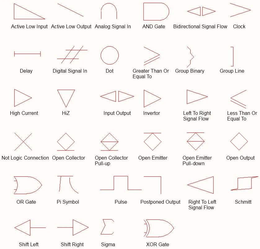
IEEE Symbols
")
A placed IEEE Symbol (Sigma)
Summary
IEEE symbols are non-electrical drawing primitives. They are used for representing logic functions or devices. These symbols enable users to understand the logic characteristics of these functions or devices without requiring specific knowledge of their internal characteristics.
Availability
IEEE Symbol objects are available for placement only in the Schematic Library Editor. A total of 34 symbols are available for placement in the following ways:
-
Choose Place » IEEE Symbols from the main menus.
-
Right-click then choose Place » IEEE Symbols from the context menu.
-
Click the
 button on the Utilities toolbar.
-
Select the Place IEEE Symbol in the Active Bar (the
Open Collector symbol will be placed).
Placement
After launching a command, the cursor will change to a cross-hair and you will enter IEEE symbol placement mode. The chosen IEEE symbol will appear floating on the cursor.
-
Position the object then click or press Enter to effect placement.
-
Continue placing further symbols or right-click or press Esc to exit placement mode.
Additional actions that can be performed during placement are:
-
Press the Tab key to pause the placement and access the IEEE Symbol mode of the Properties panel in which its properties can be changed on the fly. Click the design space pause button overlay () to resume placement.
-
Press the Spacebar to rotate the object counterclockwise or Shift+Spacebar for clockwise rotation. Rotation is in increments of 90°.
-
Press the X or Y keys to mirror the symbol along the X-axis or Y-axis.
-
Press the + or - keys (on the numeric keypad) to enlarge or shrink the symbol.
Graphical Editing
This method of editing allows you to select a placed IEEE symbol object directly in the design space and change its location or orientation graphically. IEEE symbols are fixed with respect to their shape and can be resized only through use of the relevant keyboard shortcuts. As such, editing handles are not available when the IEEE symbol object is selected.
")
A selected IEEE Symbol (Sigma)
Click anywhere inside the dashed box and drag to reposition the symbol as required. While dragging, the symbol can be rotated (Spacebar/Shift+Spacebar), mirrored (X or Y keys to mirror along the X-axis or Y-axis), or resized (+/- keys on the numeric keypad).
IEEE Symbols Properties
Location
-
(X/Y) - the current X (horizontal) and Y (vertical) coordinate of the reference point of the object, relative to the current design space origin. Edit to change the X and Y position of the object. The values can be entered in either metric or imperial; include the units when entering a value whose units are not the current default.
-
Rotation - use the drop-down to select the rotation.
Properties
-
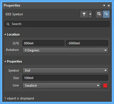
Symbol - defines the graphical IEEE symbol. Select a symbol from the drop-down list.
-
Size - the current size of the IEEE symbol. The default size is 10 DXP Default Units (100mil). Increase or decrease this value to make the symbol bigger or smaller. Entering a negative value results in the symbol appearing as if rotated by 180 degrees.
-
Line - the width of the line used to draw the outline of the symbol.
Defining Symbol Properties
Symbol properties, such as the designator and description of the symbol, are edited in the Symbol mode of the Properties panel.
-
Designator - enter the required designator prefix followed by a ?. It is recommended that the prefix consist of letters only.
-
Name and Description - these strings are helpful when symbol searches are performed.
-
Type defines what type of component this symbol represents. Non-standard components, such as a company logo (Graphical) or a heatsink (Mechanical) can be created as schematic symbols and placed into a project.
The Component Type
In a design environment, you may also need to create design entities that are not necessarily components that will be mounted on the finished PCB. For example, there might be an external module that connects to the board that you would like to draw as a component and include on the schematic for design clarity but you do not want this to be included in the BOM for this board. Or there might be mechanical hardware, such as a heat sink and mounting screw that must be included in the BOM, but you do not want to include on the schematic.
These situations are managed by setting the component's Type. For the example just described, the component type could be set to Graphical. Another special class of components is a test point – this component is required on both the schematic and the PCB. It should be checked during design synchronization but is not required in the BOM. In this case, the component Type is set to Standard (No BOM).

For a non-standard type of component, set the Type accordingly.
As well as being used to determine if a component should be included in the BOM, the Type field is also used to determine how that component is managed during component synchronization. All of the Standard, Net Tie and Jumper Types are fully synchronized, meaning the component is passed from the schematic to the PCB and the net connectivity is checked. For the Mechanical and Graphical Type, the component is not passed from schematic to PCB. If a component with one of these types has been placed manually in the PCB and the matching Type option has been chosen, then component-level synchronization is performed but no net-level connectivity checks are performed.
Refer to the Component mode of the Properties panel for detailed information about the various Type options.
Breaking the Component into Multiple Parts
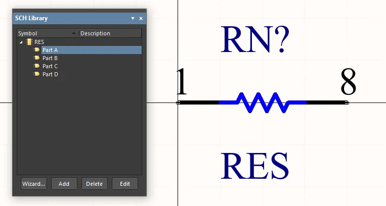
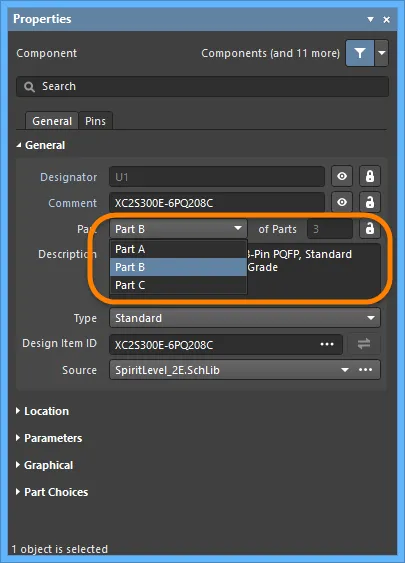
In some instances, it is more appropriate to divide the component into a number of symbols, each of which is referred to as a Part. Examples include resistor networks that contain eight individual resistors and each can be used independently of the others, the coil and contact sets in a relay, or each pin in a connector, for example, if you prefer to place connector pins throughout the sheet, rather than routing the wiring to a single connector symbol. Another example would be a 74F08SJX quadruple 2-input AND gate - in this device, there are four independent 2-input AND gates. While the component could be drawn as a single symbol showing all four gates, it would be more useful if it is drawn as four separate gates, where each gate can be placed independently of the others anywhere on the schematic.
These components are referred to as multi-part components. Each part is drawn individually in the schematic library editor, and pins are added accordingly. The image below shows the same resistor network drawn as a single part and then as four separate parts.

The same resistor network is shown as a single part on the left and as four separate parts on the right.
Notes on working with multi-part components:
-
In the schematic symbol editor, use the Tools » New Part command from the main menus to add another part to the current component. Alternatively, click the
 button on the Active Bar or right-click in the design space and choose Tools » New Part from the context menu. A new part is added to the component and a blank sheet for that part is opened and made active in the design window. Use this sheet to add the primitives that will constitute the part's graphical representation.
-
Use the SCH Library panel to move between parts in a multi-part component, as shown below.
You can also use the Tools » Next Part and Tools » Previous Part commands from the design space's right-click menu to show the next or the previous part.
-
To remove the active part from the open multi-part component in the current document, choose Tools » Remove Part from the main menus or right-click and choose Tools » Remove Part from the context menu. You can also remove parts from a multi-part component directly from the SCH Library panel.
Parts of components that have been removed cannot be restored by using the Undo command.
-
If the component parts differ slightly, you can copy and paste the content between parts and update, for example, only the pin information in new parts.
-
The schematic symbol editor allows an unlimited number of parts per component and each part may support different graphical representations, through the use of the component-level Alternate Display Mode feature. Also, a multi-part component can be represented as either a single symbol (all parts) or multiple symbols (for each part) using only a single component through defined Normal and Alternate Modes – learn more.
-
The designator of a multi-part component includes a suffix to identify each part. The suffix can be alpha or numeric and are set in the Alpha Numeric Suffix region on the Schematic - General page of the Preferences dialog. Note that this option is a software installation environment setting. It does not get stored in the library or the schematic file, and therefore, does not travel with the design files.
-
Multi-part components are considered homogeneous, that is, all parts are equivalent during design annotation and can potentially be swapped during the annotation process. For example, a relay coil might be swapped with a set of relay contacts, depending on their relative locations on the schematic sheet. To lock a specific part in a placed component, enable the  in the Properties panel as shown below.
-
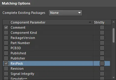
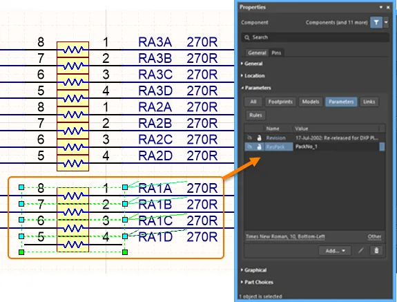
During schematic annotation, the parts in a multi-part component are packed together to complete a component in accordance with the Matching Options configured in the Annotate dialog (as shown below). The enabled checkboxes on the left determine which component properties must match for parts to be eligible to be packed together. If you need to control the packing of specific parts so they are together in the same physical component, for example, a pair of op-amps in a filter design, and do not want to assign and lock them manually, add an additional parameter to that component and enter a value that defines which parts are to be packed together. The top image below shows the Annotate dialog matching options. The enabled parameters are used for multi-part component matching, the ResPack parameter has been added in the Properties panel (bottom image) to control the packaging of resistors into packages (when the parts have the same parameter value, they can be packaged together into the same physical component). Note the Strictly option. If this option is enabled, the parts must include this parameter to be packed together. Be careful of this option if you have different types of multi-part components that you are controlling the packaging of - all of them must include that parameter if Strictly is enabled.
-
PCB part swapping can only be performed on a component whose parts are defined as a multi-part component. Learn more in the Pin Pair and Part Swapping document.
-
To define the power pins, you can create an additional part for the component and place the VCC and GND pins on that part. Remember to enable the
 option in the Properties panel to ensure that it cannot be swapped with any of the gates during re-annotation.
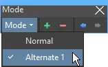
Display Modes – Multiple Presentations of the Same Component
The software supports different display representations of the same component. These representations can contain different graphical representations of the component, such as a DeMorgan or an IEEE representation. Or, for example, some of your customers might prefer to have their resistors drawn as a rectangle, while others prefer a wavy line.
Each of these representations is referred to as a display Mode. If an alternate view of a part has been added, it is displayed for editing in the schematic symbol editor by selecting the alternate mode from the Tools » Mode sub-menu in the main menus and the Mode drop-down in the Mode toolbar. The current graphical representation for the active component is denoted by an enabled 'tick' icon beside its entry in the main menus or the Mode drop-down list on the Mode toolbar. Note, however, that only the first 20 Alternate graphical modes are listed on the menu and toolbar.
In addition to selecting the normal or an alternate mode from the main menus or from the toolbar's drop-down, you can also use the Tools » Mode » Previous and Tools » Mode » Next commands from the main menus (the  and
and  buttons on the Mode toolbar) to show the previous/next mode for the active component.

A resistor created with two display modes. The library editor includes a Mode toolbar that can be used to add/remove and step through the modes.
To add an alternate view mode, with the component part displayed in the design window of the schematic symbol editor, select Tools » Mode » Add or click on the  button on the Mode toolbar. A blank sheet for
 Alternate N displays (N is the next available number in the range 1-255). Typically, you would copy the part you created in the Normal mode and paste it into the new Alternate mode. Use Edit » Copy and Edit » Paste to copy and paste the Normal mode to the Alternate mode. This gives you the correct set of pins and you can modify the graphical elements and position the pins as required.
To rename the current alternate mode, choose the Tools » Mode » Rename command from the main menus or click Rename on the Mode toolbar. After launching the command, the Rename Alternate Representation dialog will appear. Enter the new name for the selected symbol and click OK. This alternate mode will then be represented with the defined name in the main menus and in the Mode toolbar.
To remove the current graphical representation (mode) for the active component, choose the Tools » Mode » Remove command from the main menus or click the  button on the Mode toolbar. You can remove any of the graphical representations (Normal and Alternate) that exist for a component. If the component has one or more Alternate representations and you remove the Normal representation, the first Alternate (Alternate 1) will become the Normal representation. All other Alternates will be renumbered accordingly. If the component has no Alternate representations and you remove the Normal representation, the confirmation dialog will ask for confirmation to remove the component from the library - clicking Yes will effectively delete the component from the library.
The required mode is chosen when the component is placed from the library onto the schematic sheet using the Mode selector in the Graphical region of the Properties panel. The default placement mode is the mode that was displayed in the library editor when the library was last saved.
Each mode must include the same set of pins. If they do not, a warning will be generated when the project is verified. This is required because you can only define one set of pin-to-pad mappings for each footprint associated with that component. Pins do not need to be in the same location in each mode.
Use of Multi-part Components with Alternate Modes
Altium Designer supports presenting a multi-part component as either a single symbol (all sub-parts) or multiple symbols (one for each individual sub-part) using only a single component through defined Normal and Alternate Modes. For example, a dual op-amp component can be represented by two symbols in one display mode and by a single symbol in another display mode, as shown in the image below. In this case, the second part will have no primitives in the single symbol display mode.
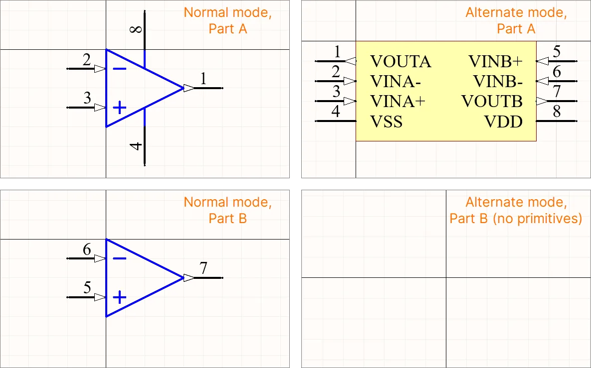
In the schematic symbol editor, parts with no primitives should be listed below all parts that have primitives in the list of symbol parts that can be seen in the SCH Library panel.
Generating a Component Report
The Component Report lists information about the active symbol.
-
Select Reports » Component (shortcut R, C).
-
A report titled <LibraryName>.cmp opens as the active document. The file includes the component name and the number of parts contained in the component. For each part, the pin details are given for each of the graphical representations (Normal and any Alternates).
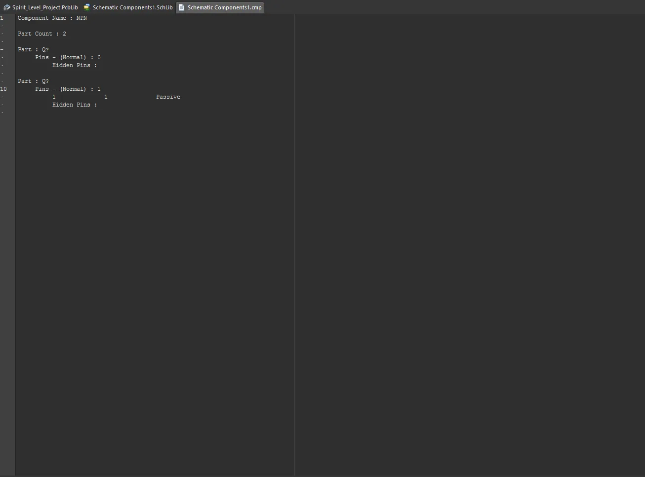
-
Close the report to return to the schematic editor design space.
Support for Jumper Components
Jumpers, also referred to as wire links, allow you to replace routing with a Jumper component, which is often an essential ingredient to successfully designing a single-sided board. Altium Designer supports use of jumper components through a special component type of Jumper.
While you can start by placing the Jumper footprints directly onto the PCB, a suggested workflow starts at the schematic. To learn more, refer to the Working with Jumper Components page.
Using the Schematic Symbol Generation Tool
The task of creating a component library symbol and its pin data has become an increasingly involved undertaking as components have advanced in complexity. With current large-scale BGA devices requiring the placement and configuration of hundreds of pins, for example, substantial time and effort are often required to create viable component symbols.
To ease the workload associated with creating component symbols, Altium Designer provides an advanced Schematic Symbol Generation Tool, based on a symbol wizard interface and pin editor dialog. This features automatic symbol graphic generation, grid pin tables and smart data paste capabilities.
To access the Schematic Symbol Generation Tool capabilities in Altium Designer, the Schematic symbol generation tool software extension must be installed. This extension is installed with Altium Designer by default. It can be installed or removed manually.
For more information about managing extensions, refer to the Extending Your Installation page (Altium Designer Develop, Altium Designer Agile, Altium Designer).
Creating a Symbol
The Schematic Symbol Generation Tool becomes available from the Schematic Library editor by choosing the Tools » Symbol Wizard command from the main menus. It can also be accessed when creating a Workspace component using the Component Editor in its Single Component Editing mode by clicking the drop-down icon on the button below the symbol model and selecting Wizard from the menu.
To create a new component symbol using the tool, first, add a new component to the active library document. The new symbol can then be developed through the tool's interface - the Symbol Wizard dialog - which opens when the command is launched. Use the dialog to interactively define the component symbol as required, including number of pins, layout of those pins, and pin data.
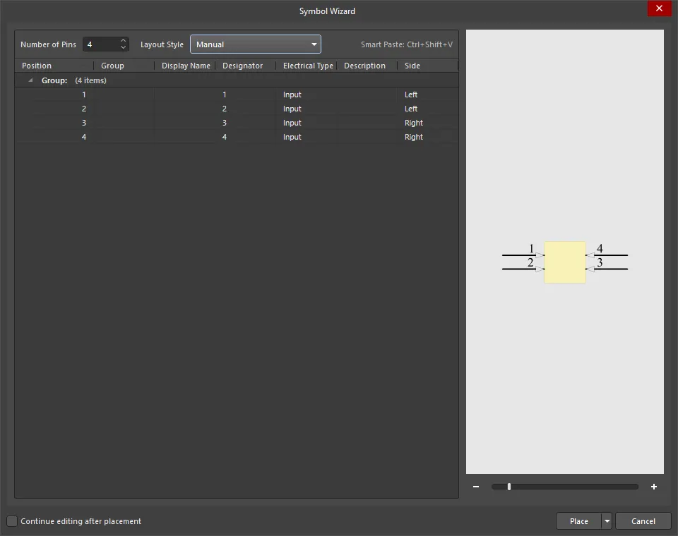
-
Number of Pins - manually type or use the up and down arrows to increase or decrease the desired number of pins.
-
Layout Style - choose from a set of predefined patterns for where the pin positioning is automatically assigned. Use the drop-down to select the preferred arrangement. The Preview image to the right and the data in the Side column will be updated accordingly. Selections include:
-
Dual in-line
-
Quad side
-
Connector zig-zag
-
Connector
-
Single in-line
-
Manual
The Manual configuration denotes that pin positions are not automatically assigned. The layout style will revert to this setting when the pin positioning of a standard style (Quad side, Connector zig-zag, and Single in-line) has been edited.
Grid
Click on a column heading to order the grid data by that column. Click again to toggle the order between ascending and descending.
Within the table, standard copy-and-paste techniques can be used to populate data from one group of cells to another. For example, you can select three cells in a column, copy the data (right-click – Copy), then select three target cells to paste the data (right-click – Paste). The same technique can be used to copy a data selection from an external source, such as a spreadsheet, text, or PDF file.
Grid cells can be manually edited on a single or multiple basis. Use standard Ctrl+click and Shift+click techniques. To edit multiple cells in columns that feature drop-down menus, select the desired cell range then make the new menu selection on one of the selected cells.
Right-click Menu
-
Move Up - use to move the selected data up one row.
-
Move Down - use to move the selected data down one row.
-
Copy - use to copy the selected data to the clipboard.
-
Paste - use to paste the most recent data that was copied to the clipboard to the cursor position.
-
Smart Paste - use to open the Pin Data Smart Paste dialog to copy several columns of external source data into matching columns in the grid. Use the dialog to configure the column data and delimiters, then click Paste. Learn more about Smart Paste.
-
Clear - use to delete the pin data.
Preview
This region displays a preview of the symbol graphic and dynamically represents the current settings and pin data. Use the slider bar or - and + to zoom in/out on the graphic.
Additional Controls
-
Continue editing after placement - if checked, the dialog will remain active (allowing further editing) once the component has been placed.
-
Place - use to place the completed symbol and pin data. Choices include:
-
Place Symbol
-
Place New Symbol
-
Place New Part
Pasting Pin Data
While the pin data in the table can be edited to a common value for multiple cells, the dialog's Paste and Smart Paste features provide an advanced way to populate all cell data by bringing in large amounts of different data from external sources.
Within the table, standard copy and paste techniques can be used to populate data from one group of cells to another. For example, by selecting three cells in a column, copying the data (right-click - Copy), then selecting three target cells to paste into (right-click - Paste).
The same technique can be used to copy and paste a data selection from an external source, such as a spreadsheet, text file, or PDF file.
 An example of pasting data copied from an external spreadsheet, into the Pin data table.
Smart Paste
Beyond standard copy and paste techniques, Smart Paste offers the capability to populate multiple columns of data from an external source, using an automated column mapping approach.
To copy several columns of source data into matching columns in the Pin data table, right-click in the table and choose the Smart Paste command from the context menu. This opens the Pin Data Smart Paste dialog, which will be populated with the source data. A range of data delimiters are available, which can be selected to match the delimiters used in the source data.

The Pin Data Smart Paste dialog
Options and Controls of the Pin Data Smart Paste Dialog
-
Delimiter - check the boxes of the delimiters that match those used in the source data. Choices include:
-
Tab
-
Semicolon
-
Comma
-
Space
-
Other
-
Data Preview - use the drop-down to select a heading for that column. The available selections are derived from the column headings in the grid region of the Symbol Wizard dialog.
The preview area dynamically updates and shows how your changes affect the text in each column.
Additional Controls
-
Paste - click to complete the smart paste process. The source data will be copied into the matching columns you specified in the grid region.
Right-Click Menu
-
Remove Line - click over a line then select this command to remove that line. If the command is performed over empty space in the dialog, the bottom line is removed.
-
Remove Column - click over a column then select this command to remove that column.
Symbol Placement
With its settings and pin data configured as required, the symbol can then be placed into the design space for the active library component. Placement can be in terms of a single component, or as one section of a multi-part component, using the respective commands available from the context menu associated to the dialog's Place button. Note that if the Continue editing after placement option is enabled, the Symbol Wizard dialog will remain active (allowing further editing) once the component/part has been placed.
When accessing the Symbol Wizard dialog for an existing component in a schematic library, all settings and pin data will be displayed, ready for further changes. The dialog will only present in its default state when used for a new library component.
Accelerating Schematic Symbol Creation with the Smart Grid Insert Tool
The Smart Grid Insert tool available in the SCHLIB List panel lets you map current clipboard data to Altium Designer object properties. These tools greatly simplify the schematic symbol creation process and in a few steps you can create the pins of a component directly from external data like a spreadsheet, a PDF, or an ASCII file.
While you could copy straight from the source pin data into Altium Designer, it is worth doing a small amount of preparatory work to achieve an optimal result. A spreadsheet is the right place to do that. Typically you will only need to perform a few steps, including:
-
Adding a header row to make the column-to-column mapping easier. Don’t worry about getting the column names exactly the same, Altium Designer does a good job of automatically inferring the correct mapping.
-
Adding an Object Kind column, so that Altium Designer knows that it is has to create pin-type objects.
-
Adding a Type column, to specify each pin’s electrical type.
-
Including X and Y pin locations. Spreadsheets have excellent tools for filling cells with values, for example if you right-click and drag to select a set of cells in Microsoft Excel, you can specify the numeric series you want, making it easy to space the pins out in the schematic library.
High-pin count and regularly sectioned components, such as FPGAs, lend themselves to implementation as multipart components in Altium Designer. The easiest way to do that is to create all the pins in the first part of the Altium Designer component, and then cut and paste the blocks of pins to the other parts.
To get the pins into neat, part-ready groups, try leaving a couple of empty rows between the pins for each part in the spreadsheet. Not only does it make it easy to see where you might need to restart coordinate values, you can also automatically add X, Y values to a large selection and then remove the redundant X, Y values in the empty rows. This will result in no pins in those deleted locations, neatly spacing the part-ready groups.

Use the tools in the spreadsheet to add suitable X and Y coordinates for the pins.
Select and copy the required cells in your spreadsheet. Don’t worry if there are columns in the selection that you don’t need, the Smart Grid tools can ignore these.
In Altium Designer, right-click in the SCHLIB List panel and select Smart Grid Insert from the menu to open the Smart Grid Insert dialog. If your source data includes a header row Altium Designer will attempt to automatically identify the object kind, then build a list of created objects. A point to keep in mind, before you map columns the list of created objects will have the properties of the current Altium Designer default pin object. So for example, if you wanted all the pins placed at 180 degrees with a length of 20, then set the default values in Altium Designer before starting the smart grid process. That way, you don’t need to worry about adding those settings into the spreadsheet or editing them in Altium Designer after the creation process. Not sure how to set the defaults? Just select Place » Pin from the menus, then before you place a pin press Tab to edit the default values, then place and delete that one pin.
Another big advantage of including a header row is that you get to use the Automatically Determine Paste button. This is a great feature – it will search and compare fields in the created object against source data column titles, and make intelligent choices about how they should be mapped. Don’t worry if the automatic feature gets one wrong, you can use the Undo Paste button to undo a mapped column. To manually map, select a column in the source data and its corresponding column in the created objects, then click the Paste Column button.
As soon as you click OK, the set of created objects will appear in the design space. Add a suitable body to each part, then cut and paste to create the individual parts, and your symbol is ready.

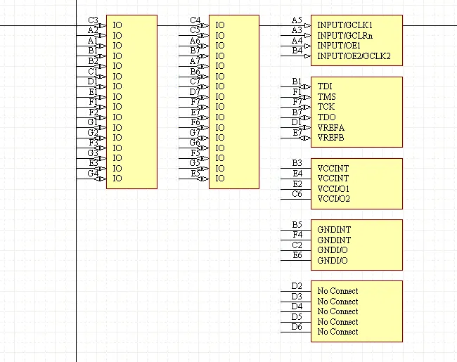
The Smart Grid Inserted pins, and the parts with the component bodies added.
