Tutorial - A Complete Design Walkthrough with Altium Designer
Welcome to the world of electronic product development in Altium's world-class electronic design software. This tutorial will help you get started by taking you through the entire process of designing a simple PCB – from idea to output files.
The Design
The design for which you will be creating the schematic and designing a printed circuit board (PCB) is a simple astable multivibrator. The circuit is shown below; it uses two general-purpose NPN transistors configured as a self-running astable multivibrator.

Circuit for the multivibrator

Animation of the designed PCB
This tutorial focuses on using Altium Designer with a connected Workspace – the most streamlined and empowered environment for your design needs. To complete this tutorial, you will need to be connected to a Workspace. It is assumed that your Workspace has been activated/installed with the sample data.
Signing In to an Altium Account
Main pages: Signing in to Your Altium Account
First, you need to connect to your Altium Account if you have not already. Your Altium Account provides access to Altium on-demand services, including a connection to an Altium 365 Workspace and manufacturer part data.
Signing In to an Altium Account in Altium Designer Develop
-
Click the Current User control at the top right of the design space and then select the
 entry from the associated menu.

-
The Sign In dialog will appear (
 ), and a new page will open in your default browser from which you can sign in to your Altium Account.
-
Once you are signed in, the Current User control will change to reflect that you have signed in to your Altium Account by displaying your Altium profile picture, or avatar (e.g.,
 ).
).

Signing In to an Altium Account in Altium Designer Agile or Altium Designer
-
Click the Current User control at the top right of the design space and then select the
entry from the associated menu.

-
In the Sign In dialog that opens, click the
 button to open a new page in your default browser from which you can sign in to your Altium Account.

-
Once you are signed in, the Current User control will change to reflect that you have signed in to your Altium Account by displaying your Altium profile picture, or avatar (e.g.,
).

-
Make sure that you are using a valid license. License selection is performed on the License Management view accessed by clicking the Current User control and selecting the
 entry from the associated menu.

Refer to the License Management in Altium Designer Agile or License Management in Altium Designer page to learn more about available license types and how to manage them.
-
Close the License Management view by right-clicking its tab at the top of the design space and selecting the Close License Management command from the context menu.

Connecting to a Workspace
Main pages: Accessing Your Workspace, Designing with a Connected Workspace
Altium Designer can connect to a Workspace to provide a single, secure data source and storage while affording unparalleled collaboration. It could be an Altium 365 Workspace (either Altium Develop Workspace or Altium Agile Workspace) – a Workspace hosted on the Altium 365 cloud-based infrastructure platform, or an Enterprise Server Workspace – a Workspace provided through the Altium On-Prem Enterprise Server, installed and managed by your own IT department.
Connecting to an Altium 365 Workspace
Click the Active Workspace control and then select the entry for the specific Altium 365 Workspace you wish to connect to from the associated menu. The Active Workspace control will change to reflect that you have connected to an Altium 365 Workspace by displaying the name of the Workspace (e.g., ![]() ).
).

Connecting to an Enterprise Server Workspace
If you use an Enterprise Server Workspace, you can connect to it from Altium Designer Agile or Altium Designer as follows:
-
Click the Current User control at the top right of the design space (e.g.,
) and then select the  entry from the associated menu.

-
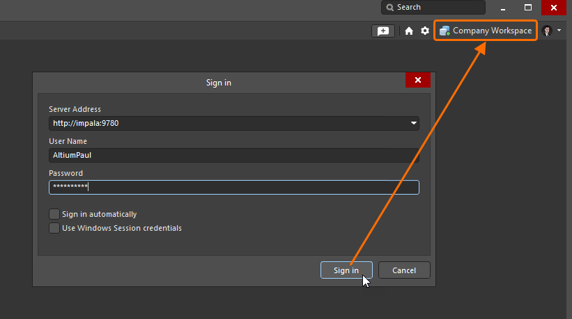
In the Sign in dialog that opens, enter the URL for the Workspace (Server Address) and your Workspace access credentials (User Name and Password), then click the
 button. The Active Workspace control will change to reflect that you have connected to an Enterprise Server Workspace by displaying the name of the Workspace.