
Capturing the Logical System Design
The essential steps for creating a multi-board system schematic design from child PCB project designs are:
-
Create a multi-board design project and add a multi-board schematic document to the project.
-
Place graphical blocks (modules) in the multi-board schematic to logically represent the child PCB projects.
-
Link each module to its appropriate child project.
-
Import the child project connectivity data into the multi-board design.
-
Add connections between modules to create the logical system design.
To add a multi-board schematic document (*.MbsDoc) to the multi-board design project, right-click the project entry in the Projects panel and then select Add New to Project » Multi-board Schematic from the context menu.
Enabling PCB Projects for Multi-board Design
Altium Designer PCB projects that represent the child board designs in a multi-board design will contain specific connections, such as edge connectors or header plugs/sockets, that are included as the electrical and physical interface to other PCBs in the system design.
These connections and their associated electrical nets need to be detected and processed by a multi-board schematic (logical) design document to establish the inter-board connectivity in the system-level design. This functionality is enabled by the presence of a specific component parameter for the PCB project connectors – a parameter named System, with Connector as the parameter value.
For each connector in a PCB project design that is intended for a system-level interconnection, select the connector part, then add the special component parameter to the list in the Parameters region under the General tab of the Properties panel when the component is selected.
To learn more about component properties, refer to the Working with Placed Components page.

The presence of the parameter named System, with a value of Connector, links this PCB connector to the multi-board schematic.
Representing Child Projects in the Multi-board Schematic
The connectivity between PCB projects that make up a multi-board design is established by placing representative blocks (modules) on the schematic and connecting their exposed connectors (module entries) together using connections.
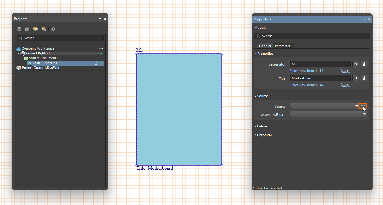
Modules, representing child PCB project designs and specific PCBs therein, are placed in the design space from the Place » Module menu.
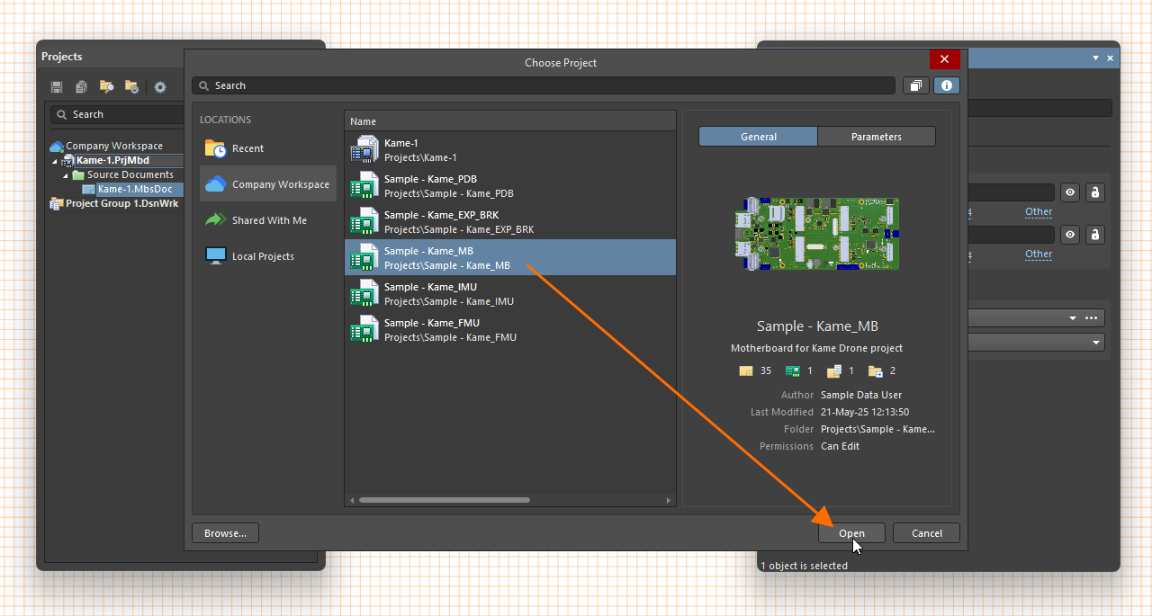
To define the source of a placed module, select it in the design space, and in the Properties panel, use the ![]() button associated with the Project field in the Source region under the General tab to open the Choose Project dialog (an incarnation of the Open Project dialog) from where you can browse to and select a PCB or multi-board project as the module's source. Once the required project is chosen, select the desired PCB board design / multi-board assembly within that project using the Assembly/Board drop-down.
button associated with the Project field in the Source region under the General tab to open the Choose Project dialog (an incarnation of the Open Project dialog) from where you can browse to and select a PCB or multi-board project as the module's source. Once the required project is chosen, select the desired PCB board design / multi-board assembly within that project using the Assembly/Board drop-down.
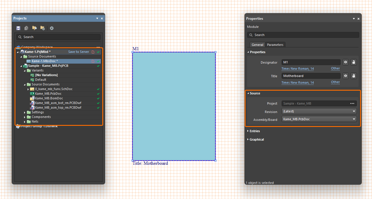
An established multi-board project features a hierarchical document structure that includes source documents and the child sub-projects linked to modules in the schematic system design. The structure of a child project is immediately added to the multi-board project when a system design module has been linked to that external project. Expand the project structure in the Projects panel to expose the constituent files in the multi-board project and its child projects.
To ensure that the multi-board project extracts and processes the correct data from its sub-projects, the PCB of each project should be synchronized with its schematic and free of design or drafting errors. To validate a PCB sub-project, right-click on its name in the panel and select the Validate PCB Project <ProjectName>.PrjPcb command – any issues will be listed in the Messages panel.
 ).
). ).
).Use the Properties panel when a placed module is selected to define other properties of the module:
-
Use Designator and Title properties in the Properties region under the General tab of the panel to specify the module's schematic identifier and title string, respectively. Use the
 button at the right of the corresponding field to toggle its visibility in the multi-board schematic and the
  button to toggle the value's ability to be edited. Use the font and Other controls to configure the string's font, position in the document, and, for the title string, the visibility of the parameter name.

-
The table in the Entries region under the General tab of the Properties panel when the module is selected will be populated when module entries are added to the module – see below.
-
Use controls in the Graphical region under the General tab of the panel to configure the display of the module: its size (width and height), the line thickness, style, and color of the module outline, and the fill color. Available line thickness and style options are defined in the Line Styles region of the Properties panel when no object is selected in the design space. For more information, refer to the Setting Up a Multi-board Schematic Document page.
-
Use controls in the Parameters tab of the panel to add, modify, and remove module parameters and configure their visibility in the design space.
Add further modules and their child project links to the multi-board schematic design, as required for the complete system design.
The modules are populated with design data from their linked project designs by importing the project data using the following commands from the main menus or the design space right-click menu:
-
Design » Import From Child Projects – propagate the design data from all source (child) projects into their specified modules.
-
Design » Import From Selected Child Projects – propagate the design data from the corresponding source (child) projects for the currently selected module(s).
Most importantly, this processes the pin and net data from each connector in the child projects that have the special System:Connector parameter attached (see details above). After the import is complete, a module entry is automatically created for each of these connectors on their respective module block graphic. The connector entry is actively associated with pins and nets on the connector in the child project. Select a module entry graphic in the design space to see its details, such as its connector pins/nets, in the Properties panel. Until connected to the entry on another module, the entry's part/pin listing in the panel will show the connector and pins as not mated.


Use the Properties panel when an entry is selected to define its properties:
-
Use controls in the Properties region under the General tab of the panel to change the value, visibility, and style of the entry's Designator and choose the entry's Type (Male/Female). In this region of the panel, the number of pins in the entry connector (Number of Pins) and the identifier number assigned to this entry in the parent module (Entry Number) are also reported.
-
Enable the System Entry option to denote the entry as a system-level connection that is not wired to another module, for example, an entry that represents a power input socket.


-
When the entry is connected using the harness or cable connection (learn more), the Mated Component region of the panel is populated with the data about the mated component.
-
In the Mated Pins region of the panel, the Pin column lists individual pins in the connector and their associated nets. Once this entry is connected, the Mated Pin column is populated with a list of the mated pins. Also, once this entry is connected, the Addresses tab of the Properties panel is populated with a tabular listing of the connection paths and nets for the entry (learn more).
-
Use controls in the Parameters tab of the panel to add, modify, and remove entry parameters and configure their visibility in the design space.
When module entries are added to a module, the table in the Entries region under the General tab of the Properties panel when the module is selected will be populated with the entries. The Part(s) column lists each module entry in terms of the designator and name of the entry connector in the source design. This can be edited for convenience – the naming is local to the multi-board design and does not affect the source child projects.

Support for External Peripherals/Components
The multi-board schematic document provides support for external peripherals/components that are not part of the regular child PCB board assemblies (i.e., 'non-PCB' components). This could include, for example, external switches, sensors, and any other off-the-shelf, third-party electronic modules. This capability is facilitated with support for two object types:
-
Custom Part – a module-like entity that provides the ability to link one or more library components and that is added to the multi-board schematic document using the Place » Custom Part command from the main menus. Use the Linked Components region of the Properties panel when the placed custom part is selected in the design space to add and remove components to the custom part using the
 and
and  buttons, respectively. If the list of linked components includes out-of-date Workspace components, click the
  button to update the components to their latest revisions. An entry is automatically added for each linked component.

-
Custom Connection – provides the ability to add a single library component to the multi-board schematic document by dragging and dropping the required component from the Components panel into free space on the sheet. An entry is automatically added for each pin of the component.


Library components are those available from your connected Workspace and available local libraries. Once placed/defined, you can connect the components to your wider design, for example, using cable and harness connections.
Cross-Probing
Cross-probing commands available in the Design main menu and the right-click menu of the design space allow you to quickly navigate from the multi-board schematic document to related elements in child projects.
-
To cross-probe from the currently selected module or entry to the PCB document or connector on that document within the PCB design project referenced by that module, use the Design » Crossprobe to PCB/Multi-board command. If the module references a multi-board assembly document (
*.MbaDoc) within a source multi-board project (*.PrjMbd), then cross-probing will be to the multi-board assembly document. -
To cross-probe from the currently selected module or entry to the top-level schematic or connector on the relevant schematic within the PCB design project referenced by that module, use the Design » Crossprobe to Schematic command.
-
To cross-probe from the currently selected module or entry to the board, or connector on that board, on the multi-board assembly document (
*.MbaDoc) within the multi-board project (*.PrjMbd), use the Design » Crossprobe to MBA command. -
To cross-probe from the currently selected harness connection on the multi-board schematic document (
*.MbsDoc) to a linked harness project (*.PrjHar), use the Design » Crossprobe to Harness command. The wiring diagram document of the associated harness project will open.
Print or Export to PDF
To print the currently active multi-board schematic document, select File » Print from the main menu (shortcut: Ctrl+P). The Print dialog will open. The left-hand side of the dialog features a scalable print preview image. Standard printing options are available on the right-hand side of the dialog. These include the ability to designate a specific printer, confirm the printer's location, view how many documents are currently in the printing queue, adjust the number of copies to print, page sizing, and orientation options. After clicking ![]() , the print set will be sent to the chosen printing device, in accordance with the options defined.
, the print set will be sent to the chosen printing device, in accordance with the options defined.

The Print dialog
To export a multi-board schematic document to a PDF file, select File » Export to PDF from the main menu.