Working with Connections
The connections established between modules in the schematic ultimately represent the connectivity between child project connectors, connector pins, and nets in the overall system design. The multi-board schematic editing environment provides comprehensive features that may be used to define, modify, check, and update that connectivity as the overall product design is developed.
Connecting Child Projects
To complete the process of creating and connecting child project modules together, place a logical connection between the entries. Multi-board connections represent the physical connections (wires, plugs and sockets, cables, or harnesses) that are used between the child board designs.
For more information about representing child projects in the multi-board schematic, refer to the Capturing the Logical System Design page.
A range of connection types is available in the Multi-board Schematic editor. The following types of connections are available:
-
A direct connection (Place » Direct Connection) is used whenever the connector on one board is to plug in directly to the connector on another without using a physical connection (cable or harness).
-
A cable (Place » Cable) is a physical connection providing a conduit for multiple signals between two boards in a multi-board system, where that cable plugs into a single connector on each of the two boards.
-
A harness (Place » Harness) is a physical connection providing a conduit for multiple signals between two or more boards in a multi-board system, where that harness can plug into one or more connectors on each of those boards.
To place a connection:
-
Select the placement command for the required type of connection.
-
The cursor will change to a cross-hair, indicating connection placement mode. Hover the cursor over an entry's connection indicator (orange circle), which will change to a green circle to indicate a valid connection point.
-
Click to confirm the connection line's starting point.
-
Reposition the cursor then click to place a series of vertex points that define the path of the connection.
-
Position the cursor over the destination entry connection point then click to complete the connection line path.
-
Continue placing further connections between other entry pairs, or right-click or press
Escto exit placement mode.
Notes on working with a placed connection:
-
The path and terminating points of a placed connection object can be graphically edited in the design space. Once selected, a connection line is highlighted in green. Click and drag a line segment in its perpendicular plane to alter the connection line path. Click and drag a connection terminating point (at a module entry) to reposition its location, then click to confirm. Normally, the connection end would be moved to another module entry, but it also can be positioned in free space where it adopts a nominal end point identifier.
-
A placed and terminated connection is automatically assigned a designator (
C_1in the example above) as an object identifier, which is editable in the connection's Properties panel. Its terminating ends are identified by their connection target information in the format<TargetModuleDesignator>-<TargetEntryDesignator>. -
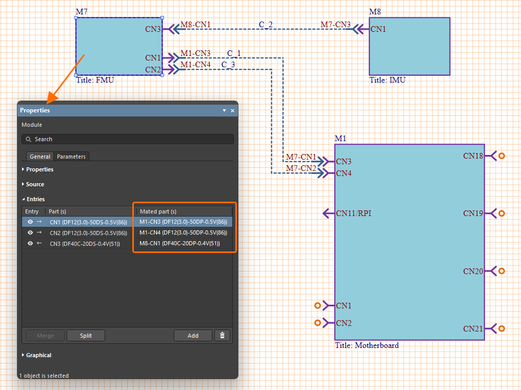
Once a module entry is connected to another entry using a connection, the Mated part(s) column in the Entries region of the Properties panel when the module is selected lists the designators and names of the parts to which the entry is connected (
 ).
).
-
A component (physical part) can be assigned to a terminating entry of a cable or harness connection. Select the terminating entry in the design space and click the
 button at the right of the Design Item ID field to select the required part using the Select Connector dialog. After clicking OK in the dialog, the name of the selected component will be shown in the Component field. If a component from your Workspace library was selected, lifecycle and revision state information will also be available in the panel (the same information is available in the Properties panel of a Workspace component placed in a PCB project schematic – refer to the Working with Placed Components page to learn more).


-
Once a connection is placed (and, for a cable or harness connection, components are assigned to its terminating entries) and a module entry or terminating entry is selected, the Mated Pin column of the table in the Mated Pins region on the General tab of the Properties panel is populated with a list of the connector entries –
 . Also, the Addresses tab of the panel provides a tabular listing of the connection paths and nets for the selected entry in terms of the part, pin, and net name of the source connection in the entry's module (the From Name column), the part, pin, and net name of the terminating connection in the 'target' module (the To Name column), the net name for the connection as either a single name or as an aggregated (
target_net/source_net) net name (the Net Name column) – .
.
-
If one end of the harness connection remains unconnected (terminated in the free space), you can enable the System Entry option in the Properties panel when the entry on this end of the connection is selected to denote the entry as a system-level connection. This can be used to make connections between multiple multi-board projects that are in a nested configuration.


Inline Connector to Harness Connections
If needed, you can define an Inline Harness Connector to create connections between harnesses. Place the connector using the Place » Entry command or ![]() on the Active Bar. A corresponding entry is created where the new entry is placed.
on the Active Bar. A corresponding entry is created where the new entry is placed.

The Assign Part Numbers to Inline Connectors dialog opens in which you can select the required parts to use with the new entries. Click the associated ![]() to select the desired connectors for each entry, then click Apply. This mates the two entries, and connection to one of the existing entries in each of the harness connections is automatically added.
to select the desired connectors for each entry, then click Apply. This mates the two entries, and connection to one of the existing entries in each of the harness connections is automatically added.

Defining Termination Type for Harness Entries
The termination type for a harness entry (a terminating end of a harness connection) can be defined. Select the harness entry in the multi-board schematic document and choose the required option from the Termination Type drop-down in the Properties region of the Properties panel's General tab. The termination type options available are:
-
Connector – the standard option used when connecting to a mating connector on the PCB. It typically involves standard board-mounted connectors.
-
Crimps/Ferrules – individual wires are terminated with crimps or ferrules before being inserted into the connector on the PCB side.
-
Wire termination – wires are blunt-cut at the harness end and either screwed down or soldered directly to the PCB. This is common with direct wire-to-board connections such as with some JST connectors.
The information is reflected in the properties for the selected harness entry and the corresponding module entry.


Editing a Connection
Select a connection graphic in the design space to see and edit its details in the Properties panel.
-
Use controls in the Properties region under the General tab of the panel to change the value, visibility, and style of the connection's Designator. In this region of the panel, the number of individual connections in the currently selected connection (Number of Connections) is also reported.
-
The Entries region provides details on attributes for each terminating end of the selected cable or harness connection. Use provided controls to toggle the corresponding entry's designator visibility and its type (the Entry column), define the designator (the Designator column), assign components used for terminating the connector ends (the Part column; similarly, components can be assigned from properties of the entry as described above). The Mated column shows the connection on the target board design to which the connection end is mated. The associated drop-down list offers other available connection targets – generally, that occupied by the other connection end.
-
Use controls in the Graphical region of the panel to configure the display of the connection, i.e., the line style and color of the connection line. Available line style options are defined in the Line Styles region of the Properties panel when no object is selected in the design space. For more information, refer to the Setting Up a Multi-board Schematic Document page.
-
Use controls in the Parameters tab of the panel to add, modify, and remove connection parameters and configure their visibility in the design space.
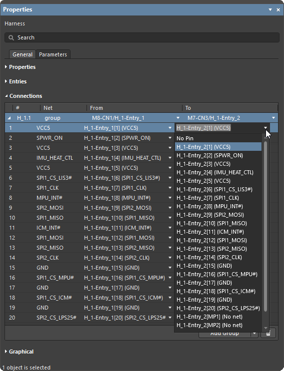
The connections between child project modules are not necessarily a pin-to-pin match, particularly when a connector is split in sections that are wired to different PCB modules. To edit or correct the pin/net matches between a module interconnection, change the From/To assignments as required in the Properties panel’s Connections list entries. Use the From or To drop-down list to select a new net assignment, and therefore a different end-to-end signal relationship through that individual connection within the module-to-module connection. For a harness connection, a pin from one connector can be connected to more than one pin on the same target connector.
To edit the individual connections within a connection, use the Connection Manager dialog (learn more).
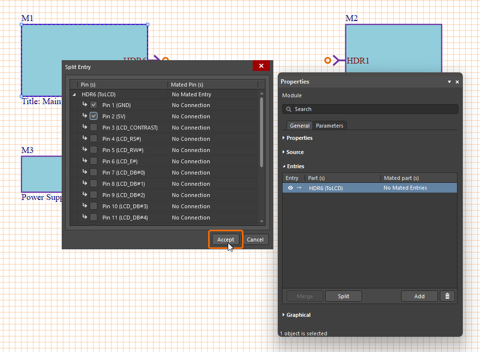
Splitting a Connection
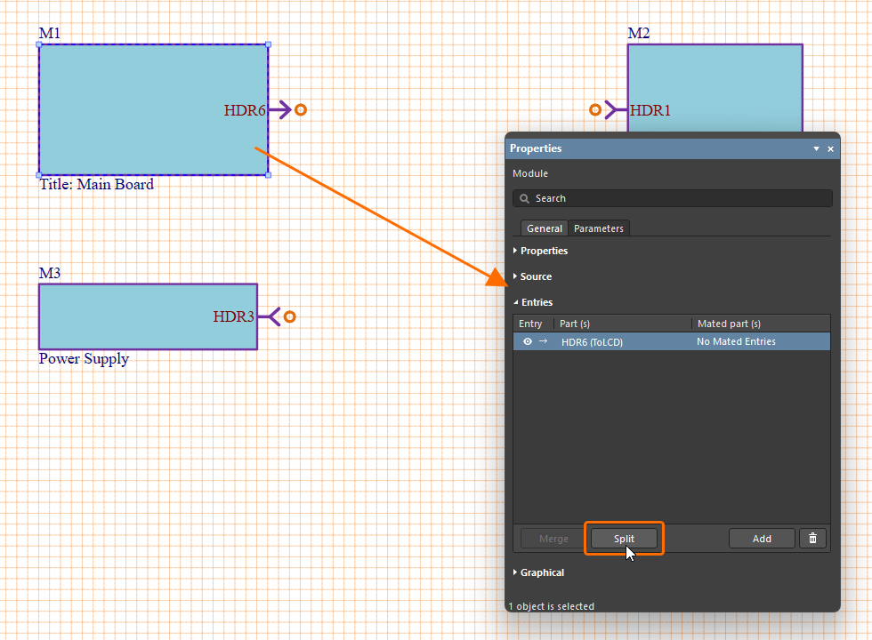
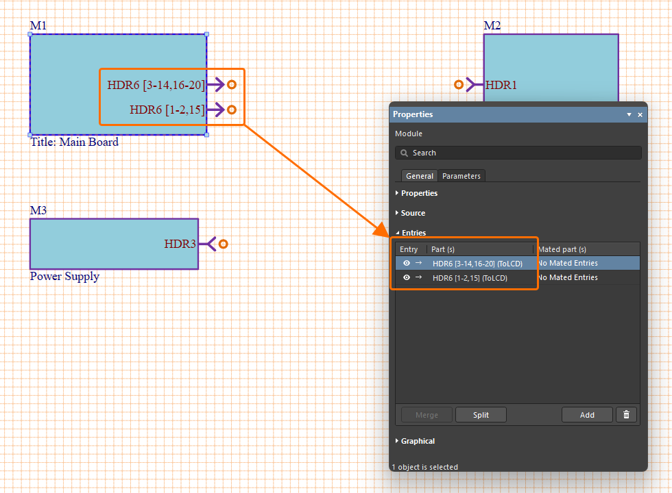
In design situations where a child project connector serves more than one connected project, the source connector can be logically divided (in terms of pins/nets) using the multi-board schematic editor’s split feature – in practice, one module is connected to two other modules. An example of such a design would be where a single header plug on a PCB is intended to accommodate two smaller header sockets, which, in turn, connect to two other PCBs – the sectioned signals from a single (e.g., 20-pin) connection are distributed to a (e.g., 10-pin) connection one PCB and a (10-pin) connection on another PCB.
|
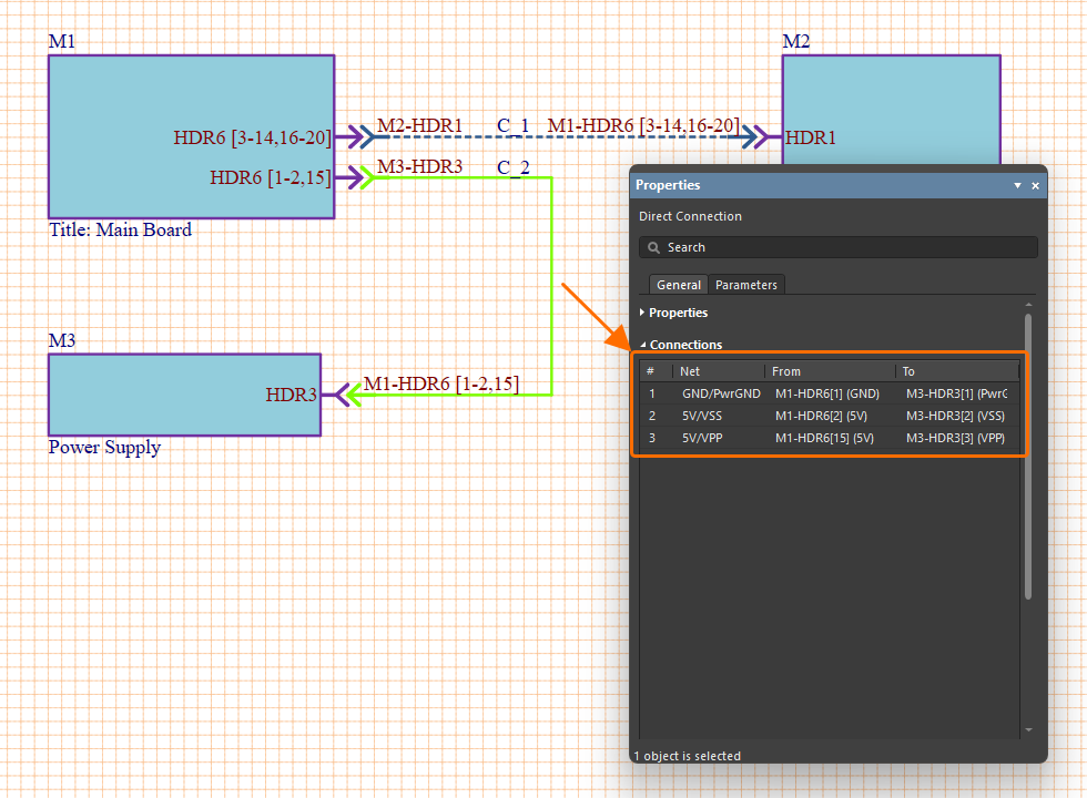
To split a connection, select the module and then an entry in the Properties panel. Click the In the subsequent Split Entry dialog, check the listed pin/net combinations you want to separate (split off) to another entry. Click the In the example shown, entry HDR6 on module M1 is intended to connect to both module M2 (a panel LCD display) and module M3 (a power supply board). The HDR6 entry connections have been split to logically separate out three power nets that will connect to HDR3 on power supply module M3. This creates an additional HDR6 entry on M1 (HDR6 [1-2,15]) that offers just the three power connections for M3, while the original HDR6 entry is automatically reassigned to offer the remaining 17 connections, which ultimately connect to HDR1 on the LCD module M2. Select a connection in the design space to see its constituent nets in the Properties panel. Here, one section of the (split) HDR6 nets is connected to HDR3 through connection C_2, which represents the three power lines between the main board (M1) and power supply (M3). As shown in the image, each virtual connection listed in the panel’s Connections region also includes its entry name, pin and net at either end in the From and To columns. |
Working with the Connection Manager
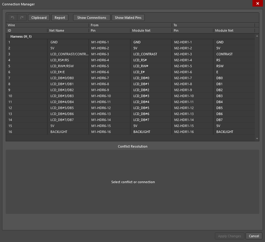
The overall connectivity in a multi-board design, once established, is detailed in the Connection Manager dialog accessed by selecting the Design » Connection Manager command from the main menus or the design space right-click menu.
The upper region of the dialog lists all net/pin assignments grouped under their parent connection designators and type (Direct, Cable, or Harness), and includes their system design ID and net name, along with their from and to pin/net connections.
The Connection Manager will highlight any connections that are considered as in conflict, or in practice, any imported connection update that does not agree with the system design editor’s existing connectivity data map (to learn more about multi-board design update, refer to the System Design Updates page). Select a highlighted net entry in the upper listing to see a graphic representation of the conflict in the dialog's lower, Conflict Resolution region, and to access a range of button options that can be used to resolve it.
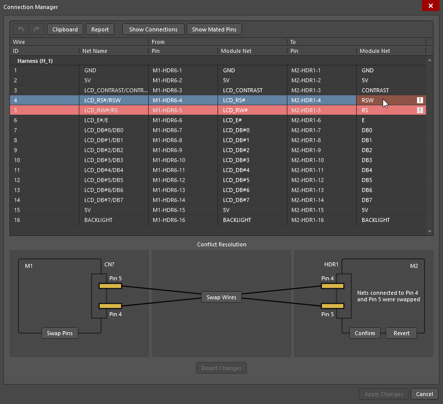
The net information shown in the highlighted fields in the Connection Manager listing represents the proposed change. In the example case shown here, the nets on HDR1 pins 4 and 5 in the child project (LCD module) are in a different order – in fact, they have been swapped.
The Connection Manager will interpret this change and offer appropriate correction action buttons on the Conflict Resolution graphic. The options include:
-
 – the nets on pins 4 and 5 for the HDR1 connector in module M2 will be changed in the multi-board design to match the updated assignments (as highlighted) in the dialog.
-
 – the current net to pin relationship for HDR1 in module M2 will be retained. The proposed change is ignored by the multi-board design. Note that the multi-board design will then not match the net assignments in the child design(s).
-
 – the pin/net assignments at the other end of the connection (at HDR6 on M1, the main board PCB) will be changed to maintain a correct net relationship between the two modules (M1 and M2).
-
 – the virtual wires that connect between HDR1 on M2 and HDR6 on M1 will be changed (swapped in this case) to correct the net connectivity conflict, and the connector pin/net assignments will not be changed. Here, wire 4 would then connect between pin 4 on HDR6 and pin 4 on HDR1, and wire 5 connect between pins HDR6-5 and HDR1-5.
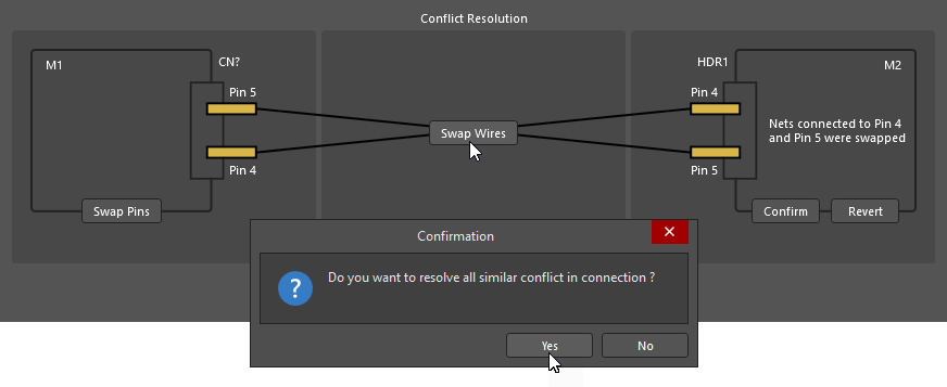
When a conflict resolution option has been selected, an affirmative answer in the following Confirmation dialog will cause the conflict resolution action to be applied to all conflicts of the same type.
The corrected net assignments will be highlighted in green and also reflected in the dialog's lower connection graphic.
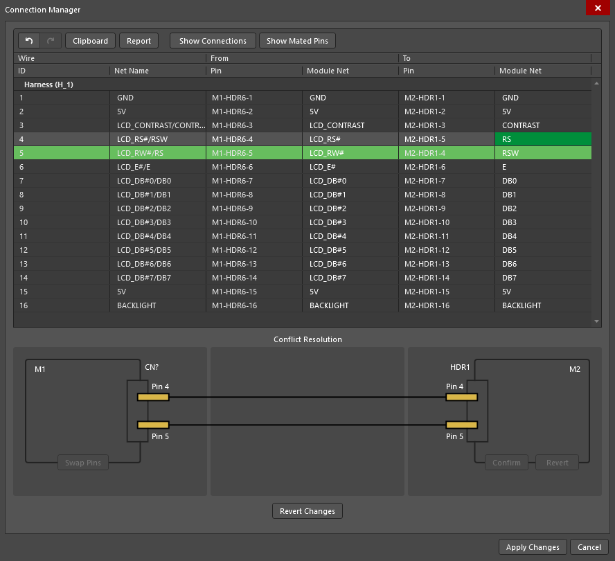
Select the ![]() button to apply the updated assignments to the multi-board design.
button to apply the updated assignments to the multi-board design.
Once the conflict resolution changes have been applied, they can be inspected in the Properties panel when the relevant connection is selected in the system design space.
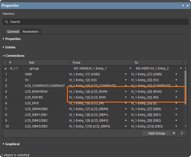
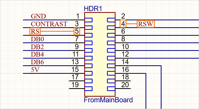
In the Properties panel image shown below, the example conflict for the H_1 connection was resolved using the ![]() option. This has effectively crossed over connections 4 and 5 so that the correct net continuity is maintained, i.e., the Reset and Read/Write nets are matched between project modules (LCD_RW# → RSW and LCD_RS# → RS, respectively).
option. This has effectively crossed over connections 4 and 5 so that the correct net continuity is maintained, i.e., the Reset and Read/Write nets are matched between project modules (LCD_RW# → RSW and LCD_RS# → RS, respectively).