To start capturing the schematic for your PCB design, add a new schematic document to the PCB project. To do this, right-click the project's entry in the Projects panel and select Add New to Project » Schematic command from the context menu (or use the File » New » Schematic command from the main menus).
Grids and Cursors
Before placing objects in the schematic editor, set the grids to enable easier placement. There are three grid types: visible grids for navigation, snap grids for placement, and electrical grids that help when creating connections. Grids are document options, meaning that they are saved with the individual design, and therefore, grid settings may differ between one design document and the next. Set the grids initially in the General region of the Properties pane, which is accessed when no objects are selected in the design space.

The Visible Grid appears whenever the zoom level allows sufficient spacing and is displayed as either lines or dots. To turn the visible grid on or off in the current document, click the toggle Visible Grid button (  ) in the panel, choose the View » Grids » Toggle Visible Grid command from the main menus, or use the
 Shift+Ctrl+G keyboard shortcut.
The Snap Grid is the grid that the cursor is locked to when placing or moving schematic design objects. The current value of the snap grid is displayed on the left-hand side of the status bar. You can also use the View » Grids » Set Snap Grid command to set a specific value for the snap grid using the ![]() Choose a snap grid size dialog.
Choose a snap grid size dialog.
Electrical grids override snap grids since they allow connections to be made to off-grid parts. Enable Snap to Electrical Object Hotspots (using the View » Grids » Toggle Electrical Grid command from the main menus or the Shift+E shortcut) so that when moving an electrical object in the design space, if it falls within the electrical grid range of another electrical object to which it could connect, it will snap to the fixed object and a hotspot (red cross) will appear. The electrical grid should be set slightly lower than the current snap grid otherwise it becomes difficult to position electrical objects one snap grid apart.
Grids can be quickly modified or toggled between enabled and disabled through keyboard or mouse shortcuts. For example, press G/Shift+G to cycle forward or back through the snap grid settings defined on the Schematic - Grids page of the Preferences dialog for the current measurement system in force (Imperial or Metric). You can also use the View » Grids » Cycle Snap Grid and the View » Grids » Cycle Snap Grid (Reverse) commands from the main menus. If you change the grid size in this manner, your entered setting (through the Choose a snap grid size dialog) will be lost since cycling only involves the currently chosen preset interval settings.
You can change the cursor type to suit your needs in the Cursor region of the Schematic - Graphical Editing page of the Preferences dialog. For example, a large 90-degree cross that extends to the edges of the design window (Large Cursor 90 option) can be useful when placing and aligning design objects.
Altium Designer components are designed on an Imperial grid. If you choose to use a metric grid, be aware that the pins will not fall on logical grid increments. You can use an Imperial grid with a Metric sheet. The sheet template and units are set in the Document Options Properties panel, which is displayed when nothing is selected on the schematic sheet.
Applying a Schematic Template to the Schematic Sheet
A schematic template is a document that holds user-defined sheet size, border and title block descriptions that can be referenced by (i.e. linked to) a schematic sheet, which removes the need to define common attributes repeatedly. Available schematic templates can be applied to the active schematic sheet document as described below.
A schematic template can be selected as a default template for new schematic sheet documents. On the Data Management – Templates page of the Preferences dialog, either hover the cursor over the required template in the list on the Templates tab and click the Set as Default control in the Default column, or click the Add button on the Defaults tab and select Schematic in the From Server menu (to choose a Workspace Schematic Template from the connected Workspace) or From File menu (to choose a schematic document file (*.SchDoc) or schematic template file (*.SchDot) from your hard drive). The default schematic template will be shown in the list on the Defaults tab of the page.
Applying a Template from the Properties Panel
The Properties panel for the active schematic document with no design objects selected in the design space displays the Document Options. In the Formatting and Size region of the Page Options section of the panel on the General tab, choose Template and then use the Template field to choose which template to use for the sheet. The list is grouped into Workspace templates (shared with you in the Workspace) and local, file-based templates.

When browsing the panel for the active schematic sheet, the Properties panel reflects the revision chosen for a schematic template. After selecting a template (or updating a template), the Update Template dialog opens that allows you to update to the current template. Afterward, an Information dialog opens, displaying that the template was updated.

The Update Template dialog
Options and Controls of the Update Template Dialog
-
Choose Document Scope – choose one of the following options to determine the scope of the update:
-
Just this document – choose to update the active schematic document only with changes to its current template.
-
All schematic documents in the current project – choose to update the active schematic document and all other schematic documents in the active project with changes to their respective current templates. Schematics that are currently closed will be opened.
-
All open schematic documents – choose this option to update the active schematic document and all other open schematic documents (regardless of parent project) with changes to their respective current templates.
-
Choose Parameter Actions – choose one of the following options to determine how parameter changes are handled:
-
Do not update any parameters – choose to leave all parameters sourced from the associated template unchanged.
-
Add new parameters that exist in the template only – choose to add any parameters that exist in the template but do not currently exist on the schematic sheet.
-
Replace all matching parameters – choose to update the value of each parameter found to exist in both the template and the schematic sheet with the value present in the template.
Note that text and graphical objects defined in the schematic template cannot be selected or edited when the template is applied to a schematic sheet. These objects become a kind of watermark.
The only aspect in which an applied template can be changed is updating the placeholder text strings set as special strings with the values of the document, project, or variant parameters by changing these values in relevant locations: the Parameters tab of the Documents Options Properties panel, the Parameters tab of the Project Options dialog, and the Edit Project Variant dialog, respectively.
Applying a Template from the Design Menu
On the Schematic editor's main Design » Sheet Templates sub-menu, you have the ability to select a different Workspace or local template.
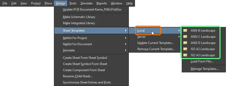
Select the Load From File command from the Design » Sheet Templates » Local sub-menu to browse and select a schematic template file on your hard drive. Select the Manage Templates command to open the Data Management – Templates page of the Preferences dialog
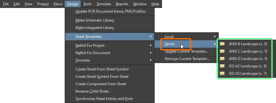
Applying a Workspace Template when Using an Environment Configuration
In addition, a Workspace schematic template can be used as a configuration data item in one or more defined Environment Configurations. When connected to the Workspace and using an environment configuration that does not control the use of schematic templates, you can manually choose a revision of a schematic template. To do so, use the Design » Sheet Templates » Set Template from server command. This opens the Choose Template dialog, in which you can browse and select the required template in the Workspace.
 schematic templates that are available to you.")
Use the Set Template from server command to manually reuse (and switch between) schematic templates that are available to you.
You can also use local schematic templates in addition to using those from your Workspace should this be required.
Updating a Template
To update a Workspace schematic template that is currently being used in the active schematic sheet to the latest revision of the associated schematic template item (or to refresh the local template that may have had its information changed in some way), use the  button next to the Template drop-down in the Document Options Properties panel or select the Design » Sheet Templates » Update Current Template command from the main menus.
Removing a Template from the Schematic Sheet
To remove the current schematic template used, choose the Design » Sheet Templates » Remove Current Template command from the main menus. After launching the command, the Remove Template Graphics dialog will open.

The Remove Template Graphics dialog
Use this dialog to define from which documents the current template will be removed - either the current document only, all schematic documents in the current (active) project (schematics that are currently closed will be opened), or all open schematic documents (regardless of parent project). After using this command, the entry for the currently used template will be blank.
When removing the current template from all schematic documents in the current project, all documents that are currently closed will be opened as the removal is performed. When removing the current template from all open schematic documents, it is removed regardless of the project to which a document belongs.
Alternatively, you can remove the template from use by switching to a different Formatting and Size mode (Standard or Custom) in the Properties panel.
Document-level Parameters
Document-level parameters can be configured for each schematic document. The document parameters are defined in the Properties panel, which is accessed when no objects are selected in the schematic. The Parameters tab of the panel is where you add, edit or delete parameters for the schematic. Use the buttons above the list of parameters to display only parameters in the list, as shown in the image below.
Adding a parameter is done by clicking the Add button and then selecting Parameter, as shown in the image below. A new parameter named Parameter n will appear in the list. Click on the name, then enter the desired parameter name. Click in the Value column then enter the desired value of the parameter.

To edit a parameter's value, click the cell in the Value column, then edit as needed.
To delete a parameter, select it in the list then click  . Within the panel, you will be asked to confirm the deletion. You can select one or more parameters in the list to delete at one time.
Properties Panel
When the active document is a schematic document (*.SchDoc) and no design object is selected in the design space, the Properties panel presents the Document Options.
The Document Options Properties panel can also be accessed by double-clicking on the sheet border.
Many of this panel's options/controls are straightforward and require no further explanation. Those that do are described in the following sections.
General Tab
Selection Filter
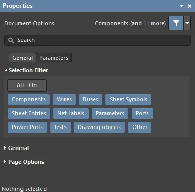
The options in this section of the panel determine which schematic objects can be selected in the design space.
General

-
Units – quickly verify the active units from the Status Bar by looking at the Grid entry at the left-hand end of the bar. To toggle between the use of mils and mm measurement units for the active schematic sheet, use the View » Toggle Units command from the main menus.
-
Visible Grid – use the eye icon to show/hide the grid in the design space.
-
Snap Grid – enter the desired grid in the text box or use the G shortcut to cycle through the different grids.
-
Snap Distance – when the cursor is within the entered distance from an enabled object snap point (and snapping is enabled for the active layer), it will snap to that point.
Page Options
Several options in this region need no explanation. The ones that do are described below.
-
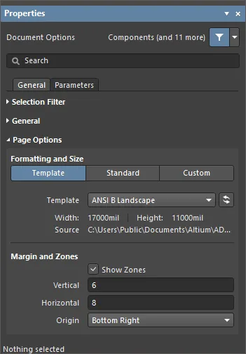
Formatting and Size
-
Template mode – set the page size and format by selecting from a range of predefined schematic sheet templates. A schematic template is a document that holds user-defined sheet size, border and title block descriptions that can be referenced by (linked to) a schematic sheet, removing the need to define these common attributes repeatedly. The list includes local and Workspace templates found in the location specified in the Data Management – Templates page of the Preferences dialog. Note that a default schematic sheet to be used for new schematic documents can be defined on that page of the Preferences dialog.
-
Template – use the drop-down menu to select from a list of Workspace and local templates, and if required, use the  button to refresh the template that may have had its information changed in some way.
-
Margin and Zones – defines the size of the sheet border graphics and its zone divisions. Uncheck the Show Zones box to hide the zone divisions in the border graphics.
-
Vertical – set the number of divisions (rows) in the vertical sheet margin. The alpha-numeric zone labeling type is defined by the Origin setting.
-
Horizontal – set the number of divisions (columns) in the horizontal sheet margin.
-
Origin – sets which corner of the document sheet(s) the perimeter zone alpha-numeric indicators will begin from (zone position
A-1 or 1-A).
-
Margin Width – set the distance (in the current units) between the page edge and each of the four border lines as indicated by the arrows associated with each entry field.
Parameters Tab
Parameters
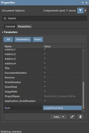
The Properties panel Parameters tab lists all available Parameters and Rules available in the current project document.
When using the
Constraint Manager functionality, note that rules added in the
Properties panel will not be detected and transferred when updating the PCB from the schematic. Only the design rules defined in the
Constraint Manager will be transferred.
-
All button – select to view both Parameters and Rules.
-
Parameters button – select to only view Parameters.
-
Rules button – select to only view Rules.
-
Parameters
-
Name and Value columns – lists the available parameters grouped by type.
When the same parameter exists in more than one location (Variant, Document, Project) and the Document parameter has no value, the parameter's value is inherited from the highest priority parameter that has a value (the parameter value defined in the schematic document overrides the value defined in the project options; the value defined in the variant overrides the value defined in the schematic document). When a Document parameter value is inherited (is being sourced from a Variant or Project parameter of the same name), the value is displayed in the Properties panel in gray italics, indicating that the parameter value is inherited. The Document parameter value can still be edited as required.
The following parameters are reserved for internal use:
-
ConfigurationParameters
-
IsUserConfigurable
While these parameters are not shown in the list, it is not possible to add user-defined parameters with these names.
-
Rules
-
Name and Value columns – these list the current specified rules and their values.
-
Add – use the drop-down menu to select to add a Parameter or a Rule. Selecting to add a new Rule will open the Choose Design Rule Type dialog to specify the type of rule to be used when adding a parameter as a rule to a supported design object in the schematic domain or a schematic document.
-
 – only accessible when a rule is selected. Click to open the Edit PCB Rule dialog to edit the selected rule.
-
 – click to delete the currently selected parameter or rule.
When a design object is selected, the panel presents options specific to that object type. The following table lists the object types available for placement on a schematic sheet. Click a link to access the properties page for that object.
