Design Directives are objects that are placed on the schematic during design capture, providing a way of specifying instructions to be passed to other parts of the software. A variety of Design Directives are available for use in the following two ways:
-
Directives associated with the automatic compilation of source schematic documents.
-
Directives used to pass information defined on a schematic sheet through to the PCB.
The following sections take a closer look at these areas and the associated directives.
Compilation-related Directives
Designs evolve over time and are captured in stages. As each stage is bedded down, it's not uncommon to want to check them in isolation from the rest of the design. Compilation of an individual schematic document (or the entire project) at intermittent stages in the capture process will often yield a number of error messages caused by circuitry that is yet to be captured or interface wiring between circuit fragments that are still incomplete. Such messages are of no real value since they only create noise around the real information. The quickest and easiest way to suppress these compilation errors is by placing No ERC or Compile Mask directives.
No ERC Directive
The No ERC directive is placed on a node in the circuit to suppress all reported Electrical Rule Check warnings and/or error violation conditions that are detected when the schematic project is validated. Refer to the Validating Your Design Project page to learn more.
Compile Mask Directive
No ERC directives are great for suppressing a low number of violating pins, ports, sheet entries, or nets within a design. But in some cases, it may be desirable to remove an entire section of the design; including components. Use a Compile Mask directive (Place » Directives » Compile Mask command) or click the Compile Mask button ( ) in the directives drop-down on the Active Bar to effectively hide the area of the design it contains from the Compiler, allowing you to manually prevent error checking for circuitry that may not yet be complete and you know will generated compile errors. This can prove very useful if you need to compile the active document, or project, to check the integrity of the design in other specific areas but do not want the 'noise' of compiler-generated messages associated with unfinished portions of the design.
As its name suggests, this directive instructs the Compiler to ignore any objects that fall completely within the bounds of the defined mask. Place the mask exactly as you would a note or rectangle object.
Consider the example schematic circuitry in the following image, where the wiring to the LCD1 device is not yet complete. Compiling just this schematic (Project » Validate PCB Project) will result in numerous violation messages (shown below), each of which is caused by the incomplete circuitry. Hover over the image to see the effect of placing a Compile Mask directive around the incomplete circuitry. These violations will be ignored by the Compiler, while the rest of the circuit on the schematic – which is completely wired – is checked. Notice that objects that are truly masked – those that completely fall within the bounding rectangle of the mask – will appear greyed-out.

Roll over the image to show the effect of using a Compile Mask directive to hide compiler violations due to incomplete circuitry.
A compile mask can be displayed in either expanded (full frame) or collapsed (small triangle) modes. These modes correspond to the mask being enabled and disabled, respectively. Toggle the display mode by clicking on the top-left corner of a placed compile mask. This feature can be helpful when simulation is included as part of the design flow:
learn more.
While compile masks can be rotated or mirrored along the X or Y axis, this has no effect on the orientation of the design circuitry within.
Compile Mask
 A placed Compile Mask, shown on the left side of the above schematic.
Summary
A Compile Mask is a design directive that is used to effectively hide the area of the design it contains from the Compiler when performing validation using the Project » Validate Project command. It provides a way to manually prevent error checking for circuitry that may not yet be complete and will generate validation errors. The Compile Mask is useful in circumstances where the current project needs to be validated to check the integrity of the design in other specific areas, but the clutter of compiler-generated messages associated with unfinished portions of the design is not desired.
Although called a 'Compile Mask', this directive is not associated with the act of compilation - which is automatically performed after each user operation, courtesy of Altium Designer's Dynamic Compilation feature. Rather, the Compile Mask comes into play when you manually run a validation of the project, which is separate and distinct to compilation, and a process that requires to be manually instigated by the user. Validation then checks the schematic documents within the project for electrical and drafting errors, in conjunction with settings defined on the
Error Reporting and
Connection Matrix tabs of the
Project Options dialog.
Availability
Compile Masks are available for placement in the Schematic Editor only. To place a Compile Mask:
-
Click the Place » Directives » Compile Mask command from the main menus.
-
Click the Compile Mask button (
 ) in the directives drop down on the Active Bar located at the top of the design space. Click and hold an Active Bar button to access other related commands. Once a command has been used, it will become the topmost item on that section of the Active Bar.
-
Right-click in the schematic editor then click Place » Directives » Compile Mask.
Placement
After launching the command, the cursor will change to a cross-hair indicating Compile Mask placement mode. Placement is made by performing the following sequence of actions:
-
Position the cursor then click or press Enter to anchor the first corner of the mask.
-
Move the cursor to adjust the size of the mask so that it completely encapsulates the area of the design that needs to be hidden from the Compiler, then click or press Enter to anchor the diagonally-opposite corner and complete placement of the mask. Design objects falling completely within the bounds of the mask will become grayed-out.
-
Continue placing further compile masks or right-click or press Esc to exit placement mode.
Graphical Editing
This method of editing allows you to select a placed compile mask object directly in the design space and change its size, shape or location graphically.
A compile mask can be displayed in either active (full frame) or collapsed (boxed triangle) modes, which correspond to the mask being enabled and disabled, respectively. Toggle the display mode by clicking on the ▲ or ▼ icon in the top-left corner of a placed compile mask.
 a compile mask.") Click the triangle in the top-left corner to collapse (and disable) a compile mask.
Click the triangle in the top-left corner to collapse (and disable) a compile mask.
When an active (expanded) compile mask object is selected, the following editing handles are available:
.") A selected Compile Mask (when active).
A selected Compile Mask (when active).
-
Click and drag A to resize the compile mask in the vertical and horizontal directions simultaneously.
-
Click and drag B to resize the compile mask in the vertical and horizontal directions separately.
-
Click anywhere on the compile mask – away from editing handles – and drag to reposition it. While dragging, the compile mask can be rotated (Spacebar/Shift+Spacebar) or mirrored (X or Y keys to mirror along the X-axis or Y-axis, respectively).
Note that when a Compile Mask is in its collapsed state, only its position may be graphically changed by dragging it to a new location.
If attempting to graphically modify an object that has its Locked property enabled, a dialog will appear asking for confirmation to proceed with the edit. If the Protect Locked Objects option is enabled on the Schematic – Graphical Editing page of the Preferences dialog, and the Locked option for that design object is enabled as well, then that object cannot be selected or graphically edited. Click the locked object to select it then disable the Locked property in the List panel or disable the Protect Locked Objects option to graphically edit the object.
Non-Graphical Editing
The following methods of non-graphical editing are available.
Editing via the Compile Mask Dialog or Properties Panel
Panel page: Compile Mask Properties
This method of editing uses the associated Compile Mask dialog and the Properties panel mode to modify the properties of a Compile Mask object.
After placement, the Compile Mask dialog can be accessed by:
-
Double-clicking on the placed compile mask object.
-
Selecting the compile mask object, right-clicking, then choosing Properties from the context menu.
During placement, the Compile Mask mode of the Properties panel can be accessed by pressing the Tab key. Once the compile mask is placed, all options appear.
After placement, the Compile Mask mode of the Properties panel can be accessed in one of the following ways:
-
If the Properties panel is already active, by selecting the compile mask object.
-
After selecting the compile mask object, select the Properties panel from the Panels button in the bottom right section of the design space or by selecting View » Panels » Properties from the main menu.
If the
Double Click Runs Interactive Properties option is disabled (default) on the
Schematic - Graphical Editing page of the
Preferences dialog, when the primitive is double-clicked or you right-click on a selected primitive then choose
Properties, the dialog will open. When the
Double Click Runs Interactive Properties option is enabled, the
Properties panel will open.
While the options are the same in the dialog and the panel, the order and placement of the options may differ slightly.
Editing Multiple Objects
The Properties panel supports multiple object editing, where the property settings that are identical in all currently selected objects may be modified. When multiples of the same object type are selected manually, via the Find Similar Objects dialog or through a Filter or List panel, a Properties panel field entry that is not shown as an asterisk (*) may be edited for all selected objects.
Editing via a List Panel
Panel pages: List Panels, SCH Filter
A List panel displays design object types from one or more documents in tabular format, enabling quick inspection and modification of object attributes. Used in conjunction with appropriate filtering – by selecting object types (using the panel's Include options), or by using the applicable Filter panel or the Find Similar Objects dialog – it enables the display of just those objects falling under the scope of the active filter. The properties for the listed objects may then be edited directly in the List panel.
Compile Mask Properties
Schematic Editor object properties are definable options that specify the visual style, content and behavior of the placed object. The property settings for each type of object are defined in the following way:
-
Post-placement settings – all Compile Mask object properties are available for editing in the Compile Mask dialog and the Properties panel when a placed Compile Mask is selected in the design space.
While the options are the same in the dialog and the panel, the order and placement of the options may differ slightly.
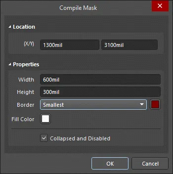
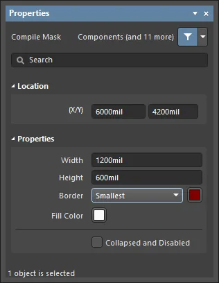
Location
-
(X/Y)
-
X (first field) - the current X (horizontal) coordinate of the reference point of the object, relative to the current design space origin. Edit to change the X position of the object. The value can be entered in either metric or imperial; include the units when entering a value whose units are not the current default.
-
Y (second field) - the current Y (vertical) coordinate of the reference point of the object, relative to the current origin. Edit to change the Y position of the object. The value can be entered in either metric or imperial; include the units when entering a value whose units are not the current default.
Properties
-
Width - enter the width of the object.
-
Height - enter the height of the object.
-
Border - use the drop-down to select the desired border.
-
Fill Color - click the color box to select the desired color for the object.
-
Collapsed and Disabled - check the box to collapse and disable the object.
PCB-related Directives
As a Unified Design Environment, Altium Designer provides the ability for PCB requirements to be defined prior to laying out the board. This is achieved by adding and specifying parameters to objects placed on the schematic sheet(s).
For certain schematic design objects – such as components, sheet symbols, ports, etc – this involves adding the relevant parameter(s) as part of that object's properties. For net objects such as wires and buses, parameters cannot be added directly as a property of the wire or bus. Instead, the parameters required to hold the information are specified using dedicated design directives.
The following information can be specified, using directives, and will be transferred to the appropriate PCB-based definitions during design synchronization:
-
PCB layout constraints
-
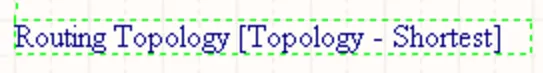
Differential pairs
-
Net classes
By including design directives within the Schematic, design engineers can specify explicit design constraints, and it ensures the Schematic remains the master record of the design. Any amendments to the design would be carried out on the schematic side only and pushed across to the PCB. This can become particularly important when multiple people are working on the design – especially if they are geographically separated. Rather than attempting to communicate with one another through chains of emails, or phone calls, the person capturing the design can ensure that particular constraints are indeed used during the layout phase.
At the heart of this functionality is the Parameter Set directive.
These are essentially user-defined Parameter Set objects, which can be associated with a net object within a schematic design. Place a PCB Layout directive on a wire, bus, or signal harness, to define one or more design constraint targeting the associated net(s). When a PCB is created from the schematic, the information in the PCB layout directive is used to create relevant PCB design rules. The information specified by a PCB Layout directive is applied only to the net (or set of nets) to which the directive is connected.

A Parameter Set directive.
This acts as a container for any number of parameters targeting the net that the Parameter Set directive is attached to. A default Parameter Set directive that has no parameters can be placed (Place » Directives » Parameter Set) and the relevant parameter(s) can be added later. The following sections take a closer look at using these parameter-based directives. Both user-defined (Parameter Set) and pre-defined (Differential Pair) parameter set directives are available. The only difference between an empty parameter set and a pre-defined parameter set is that the pre-defined parameter sets include a parameter, as will be described below.
Moving from Directives to the Constraint Manager
The original approach to defining the design requirements was to handle them separately in the schematic and PCB editors; Directives define them in the schematic editor, and Design Rules in the PCB editor. This separation has been resolved with the introduction of the Constraint Manager, a separate editor for defining the design requirements, allowing them to be configured and edited at any stage of the design process. Only one approach can be used for a given project; an easy way to check is to look for a Constraint Manager entry in the Design menu. If there is not (and instead there is a Rules entry in the PCB editor Design menu), then the project is using the older Design Rules approach.
If the Constraint Manager is being used, net classes, differential pairs, differential pair classes, and rules defined using the parameter set and differential pair directives will not be detected and transferred when updating the PCB from the schematic. Only the net classes, differential pairs, differential pair classes, and rules defined in the Constraint Manager will be transferred.
Note that you can import rules, net classes, differential pairs, and differential pair classes from directives placed in schematics, using the Import from Directives command from the right-click menu of the Physical or Electrical view of the Constraint Manager when accessed from schematics – learn more. Note that after importing data from directives to the Constraint Manager and saving those changes, the imported directives will be distinguished in the schematic design space by their blue coloring (with a slightly different symbol). This indicates that the one-way transition from directives to the Constraint Manager has occurred, with the blue directives becoming read-only objects (no further editing is allowed).
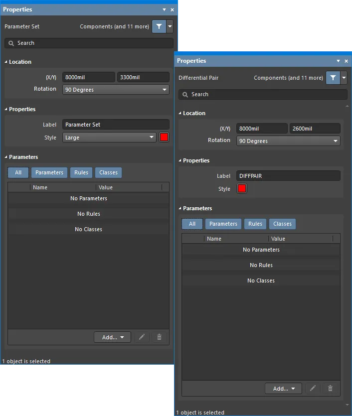
Parameter Set

A Parameter Set
Summary
A parameter set is a design directive that allows design specifications to be associated with a net-type object within a schematic design. For example, use a parameter set to declare two nets to be members of a differential pair. It is the presence of specifically named parameters in the parameter set that the software uses to determine which design directive you are placing.
Availability
Parameter sets are available for placement in the schematic editor only. Both default (empty) and pre-defined (Differential Pair) parameter set directives are available. The only difference between an empty parameter set and a pre-defined parameter set is that the pre-defined parameter sets include a parameter, as described below.
Access the corresponding commands from the main Place menu as follows:
| • |
Place » Directives » Parameter Set |
 |
| • |
Place » Directives » Differential Pair |
 |
Placement
A parameter set can be used to attach parameters to a:
-
Wire
-
Bus
-
Signal harness
-
Sheet Symbol
After launching the command, the cursor will change to a cross-hair and you will enter design directive placement mode. Placement is made by performing the following actions:
-
Position the cursor over a wire or other net object and click or press Enter to place.
-
Continue placing further directives or right-click or press Esc to exit placement mode.
Additional actions that can be performed during placement – while the parameter set is still floating on the cursor are:
-
Press the Tab key to pause the placement and access the Parameter Set mode of the Properties panel, from where its properties can be changed on the fly. Click the design space pause button overlay ( ) to resume placement.
-
Press the Alt key to constrain the direction of movement to the horizontal or vertical axis, depending on the initial direction of movement.
-
Press the Spacebar to rotate the arc counterclockwise or Shift+Spacebar for clockwise rotation. The action can also be performed while dragging the object. Rotation is in increments of 90°.
-
Press the X or Y keys while in placement mode to flip the parameter set along the X-axis or Y-axis.
While attributes can be modified during placement (
Tab to bring up the
Properties panel), keep in mind that these will become the default settings for further placement unless the
Permanent option on the
Schematic – Defaults page of the
Preferences dialog is enabled. When this option is enabled, changes made will affect only the object being placed and subsequent objects placed during the same placement session.
Graphical Editing
This method of editing allows you to select a placed parameter set directive directly in the design space and change its location or orientation graphically.
When a parameter set directive is selected in the design space, a dashed box will appear around the directive. The box encloses the area occupied by the directive only. For each visibility-enabled member parameter of the set, a dashed line will be visible, connecting the text field of the parameter to the body of the directive, which affirms association:
Click anywhere inside the dashed box then drag to reposition the parameter set as required. While dragging, the parameter set can be rotated (Spacebar/Shift+Spacebar) or mirrored (X or Y keys to mirror along the X-axis or Y-axis).
The parameter set's text fields (which can be graphically edited independently of the parent directive) can only be adjusted with respect to size by changing the Style option on the Schematic – Defaults page of the Preferences dialog. As such, editing handles are not available when any of these objects are selected.
Click anywhere inside the dashed box then drag to reposition the text object as required. While dragging, the text object can be rotated (Spacebar/Shift+Spacebar) or mirrored (X or Y keys to mirror along the X-axis or Y-axis).
If the Enable In-Place Editing option is enabled on the Schematic – General page of the Preferences dialog. You will be able to edit the value for a parameter directly in the design space (with the exception of parameters that have been added as rules). Select the text object and then click once to invoke the feature. Type the new value as required and then click away from the text object or press Enter to effect the change.
If attempting to graphically modify an object that has its Locked property enabled, a dialog will appear asking for confirmation to proceed with the edit. If the Protect Locked Objects option is enabled on the Schematic – Graphical Editing page of the Preferences dialog, and the Locked option for that design object is enabled as well, then that object cannot be selected or graphically edited. Click the locked object to select it then disable the Locked property in the List panel or disable the Protect Locked Objects option to graphically edit the object.
Non-Graphical Editing
The following methods of non-graphical editing are available.
Editing via the Parameter Set Dialog or Properties Panel
Panel page: Parameter Set Properties
This method of editing uses the associated Parameter Set dialog and the Properties panel mode to modify the properties of a parameter set object.

The Parameter Set dialog on the first image, and the Parameter Set mode of the Properties panel on the second image
After placement, the Parameter Set dialog can be accessed by:
-
Double-clicking on the placed parameter set object.
-
Placing the cursor over the parameter set object, right-clicking then choosing Properties from the context menu.
During placement, the Parameter Set mode of the Properties panel can be accessed by pressing the Tab key. Once the parameter set is placed, all options appear.
After placement, the Parameter Set mode of the Properties panel can be accessed in one of the following ways:
-
If the Properties panel is already active, by selecting the parameter set object.
-
After selecting the parameter set object, select the Properties panel from the Panels button at the bottom right of the design space or select View » Panels » Properties from the main menu.
If the
Double Click Runs Interactive Properties option is disabled (default) on the
Schematic – Graphical Editing page of the
Preferences dialog, when the primitive is double-clicked or you right-click on a selected primitive then choose
Properties, the dialog will open. When the
Double Click Runs Interactive Properties option is enabled, the
Properties panel will open.
The Parameter Set properties can be accessed prior to entering placement mode from the
Schematic – Defaults page of the
Preferences dialog. This allows the default properties for the object to be changed, which will be applied when placing subsequent objects.
Editing Multiple Objects
The Properties panel supports multiple object editing, where the property settings that are identical in all currently selected objects may be modified. When multiples of the same object type are selected manually, via the Find Similar Objects dialog or through a Filter or List panel, a Properties panel field entry that is not shown as an asterisk (*) can be edited for all selected objects.
Editing via a List Panel
Panel pages: List Panels, SCH Filter
A List panel allows you to display design objects from one or more documents in tabular format, enabling quick inspection and modification of object attributes. Used in conjunction with appropriate filtering – by using the applicable Filter panel or the Find Similar Objects dialog – it enables the display of just those objects falling under the scope of the active filter – allowing you to target and edit multiple design objects with greater accuracy and efficiency.
Notes
-
When placing a default parameter set directive, there will be no existing parameters. Once placed, add the relevant parameter(s) to it through the Parameters section of the Properties panel.
-
A parameter set directive allows you to assign PCB layout information to a net in the schematic. When a PCB is created from the schematic, the information in the Parameter Set is used to create relevant PCB design rules. The information specified by a Parameter Set directive is applied only to the net(s) to which it is connected.
-
When a parameter set directive is added to a net, the Power Net and High Speed fields are available in the net's Properties panel. When updating the PCB document from schematics, the Supply Nets design rule is suggested to be added to each net with the Power Net parameter enabled.
-
Net Class directives enable you to create user-defined net classes on the schematic. When a PCB is created from the schematic, the information in a Net Class directive is used to create the corresponding Net Class on the PCB. To make a net a member of a net class, attach a parameter set directive to the relevant wire or bus and a class whose name is set to the desired class. The Generate Net Classes option (for User-Defined Classes) must be enabled on the Class Generation tab of the Project Options dialog to use this feature.
-
If a Net Class directive has been defined for a net, then any PCB design rules that are also created by that parameter set object will have a rule scope of Net Class when the design is transferred to the PCB editor.
-
A Net Class directive can be created from your placed Parameter Set directive by adding a class that must have its value set to the required PCB Net Class.
-
A Blanket, in conjunction with a Parameter Set directive, can also be used for applying component classes and parameters for components that are completely within the area defined by the Blanket. To do this, use the Component Class and Parameter options from the Add button drop-down in the properties of the Parameter Set directive attached to the Blanket. The information about the component class and parameter will be transferred to the project PCB document during the ECO process when updating the PCB.
Parameter Set Properties
Schematic editor object properties are definable options that specify the visual style, content and behavior of the placed object.
The property settings for each type of object are defined in two different ways:
-
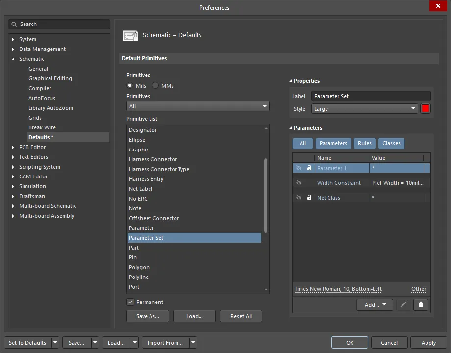
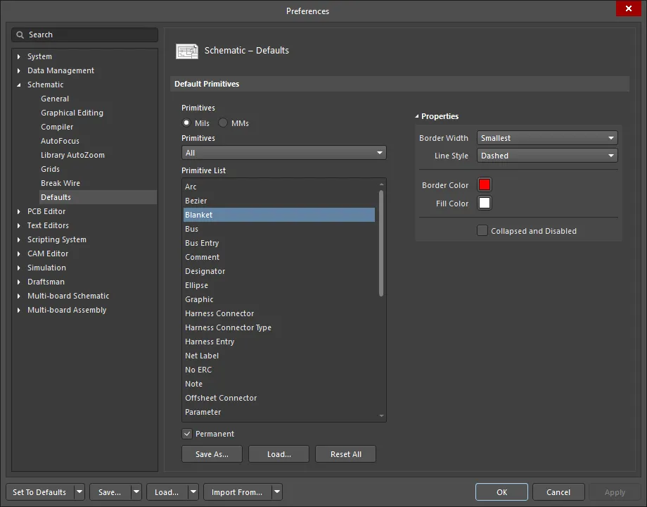
Pre-placement settings – most Parameter Set object properties, or those that can logically be pre-defined, are available as editable default settings on the Schematic – Defaults page of the Preferences dialog (accessed from the  button at the top-right of the design space). Select the object in the Primitive List to reveal its options on the right.
-
Post-placement settings – all Parameter Set object properties are available for editing in the Parameter Set dialogs and the Properties panel when a Parameter Set is selected in the design space.
If the
Double Click Runs Interactive Properties option is disabled (default) on the
Schematic – Graphical Editing page of the
Preferences dialog, when the primitive is double-clicked or you right-click on a selected primitive then choose
Properties, the dialog will open. When the
Double Click Runs Interactive Properties option is enabled, the
Properties panel will open.
While the options are the same in the dialog and the panel, the order and placement of the options may differ slightly.
In the below properties listing, options that are not available as default settings in the Preferences dialog are noted as "Properties panel only".
Location
-
(X/Y)
-
X (first field) – the current X (horizontal) coordinate of the reference point of the object, relative to the current design space origin. Edit to change the X position of the object. The value can be entered in either metric or imperial; include the units when entering a value whose units are not the current default.
-
Y (second field) – the current Y (vertical) coordinate of the reference point of the object, relative to the current origin. Edit to change the Y position of the object. The value can be entered in either metric or imperial; include the units when entering a value whose units are not the current default.
-
Rotation – use the drop-down to select the rotation.
Properties
-
Label – the parameter set label. Edit if desired.
-
Style – use the drop-down to select the style. Click on the color box to access a drop-down from which you can select the default color.
Parameters
-
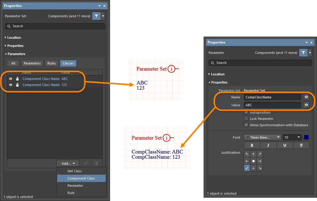
Grid – lists the Name and Value of the parameters associated with the currently selected parameter. Once added, the Name and Value fields may be edited. The Value can be named by clicking on the field and entering the desired text. The Name field may only be changed when in the Properties panel mode of the Parameter Set object by using Ctrl+Click. This method opens the Parameter mode of the Properties panel, where you can enter the desired name within the Name field. Use the lock icon (
 ) to lock/unlock a listed parameter. Use the eye icon to show/hide the parameter. All, individual, or no parameters can be displayed within this region by toggling the All and individual parameter buttons. The parameters are disabled when their respective buttons are gray and enabled when their respective buttons are blue.
-
Add – use the drop-down to add a type of class:
-
Net Class – select to add a new net class.
-
Component Class – select to add a new component class. This option is accessible in the Parameter Set iteration of the Parameter Set dialog or Properties panel only.
You may add a new class Component Class Name to set parameters for components within a blanket. Associating the Component Class Name to a component (or group of components) will result in sending the information about the component class, its name and members to the PCB as is done currently for Net Classes.
-
Diff. Pair Net Class – select to add a new differential pair net class. This option is accessible in the Differential Pair iteration of the Parameter Set dialog or Properties panel only.
-
Parameter – select to add a new parameter.
-
Rule – click to open the ![]() Choose Design Rule Type dialog in which you can choose a new rule. After choosing a new rule then clicking OK, the Edit PCB Rule (From Schematic) dialog opens so that you can edit the new rule if desired.
Choose Design Rule Type dialog in which you can choose a new rule. After choosing a new rule then clicking OK, the Edit PCB Rule (From Schematic) dialog opens so that you can edit the new rule if desired.
Note that after synchronizing data by
importing data from directives to the Constraint Manager and saving changes in the
Constraint Manager, the controls to add a new or edit/remove an existing net class, diff pair class, component class, or rule will be grayed out in the
Properties panel for the corresponding directives. Entries imported to the
Constraint Manager will essentially become read-only in directive properties, and you will be able to filter them out using the
Constraint Manager button at the top of the
Properties panel's
Parameters region.
Click the pencil ( ) icon to open the Edit PCB Rule (From Schematic) dialog to edit the selected item. Click
  to delete the selected item.
-
Font Settings – click on the displayed font to change the font style. This option is only available once a net class, differential pair net class, parameter, or rule has been added.
-
Other – If a net class, differential pair net class, parameter, or rule has been added, click to open a drop-down to change additional options:
-
Show Parameter Name – enable to show the parameter name.
-
Allow Synchronization with Database – enable to synchronize with the database.
-
X/Y – enter the X and Y coordinates.
-
Rotation – use the drop-down to select the rotation.
-
Autoposition – check to enable auto-positioning.
Placing Parameter Set Directives
Place a directive of this type by choosing the Place » Directives » Parameter Set command from the main menu, or when right-clicking within the design space. When placing a default parameter set directive, there will be no existing parameters. A parameter set is a design directive that allows design specifications to be associated with a net-type object within a schematic design. For example, use a parameter set to declare two nets to be members of a differential pair. It is the presence of specifically named parameters in the parameter set that the software uses to determine which design directive you are placing.
In addition to user-defined parameter directives, a rule-based parameter directive is defined from the Choose Design Rule Type dialog, accessible from the parameter's associated Properties panel mode. Access involves the following:
-
Press Tab before placing the Parameter Set or double-click an already placed Parameter Set directive to display the Parameter Set mode of the Properties panel.
-
Next, click the Add button in the Parameters section of the Parameter Set mode of the Properties panel and choose Rule from the drop-down to select a rule from the Choose Design Rule Type dialog.

Editing the value for a rule.
Use the Choose Design Rule Type dialog to choose the rule that you wish to add as a rule parameter to the directive. Double-clicking on a rule type will give you access to the relevant Edit PCB Rule (From Schematic) dialog in which you can define the constraints for the rule.
The specific properties that are present in the Edit PCB Rule (From Schematic) dialog are dependent upon the selected design rule, and will be the same as the properties that are defined for that rule in the PCB editor.
For example, the image below shows the Edit PCB Rule (From Schematic) dialog for the Max-Min Width Rule, where you can: configure Min/Preferred/Max settings for all layers, manually define each width setting for each layer, or choose to use an Impedance Profile. If you are selecting an impedance profile and the actual physical board structure has already been defined in the PCB editor, you can also select the board file to Load the PCB Layer Stack and calculate the track width values.
 If the PCB exists and the layer stack has been defined, the calculated widths can be loaded into the schematic.
The rule shown above was applied to a class of nets. This was achieved by placing a Blanket Directive with a PCB Routing Directive attached to group the nets into a class, and then apply the Max-Min Width Rule to that class (show image![]() ).
).
For detailed information about each of the PCB Design Rules and constraints, click here.
Use the Measurement Units drop-down field to select Metric or Imperial units.

Specifying the constraints for a chosen rule.
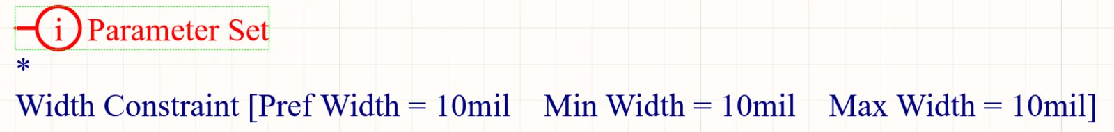
The entry for the Parameters region will be the rule type chosen, along with the specified constraints. The following image illustrates the defined width constraint rule parameters for a Parameter Set directive. To display the rule within the design space, click the visibility ( ) icon within the Rules region.

Multiple rule constraints defined for a particular net, courtesy of a Parameter Set directive.
When the design is transferred to the PCB, through the synchronization process, the relevant design rules will be created, based on the information contained within a directive. The word Schematic is used in the name for each generated rule, to distinguish the source of that rule.

Generated design rules on the PCB side.
Remember that multiple parameters can be added to the same Parameter Set directive, allowing for a neater schematic.
Placing Net Class Directives
A Net Class directive enables you to create user-defined net classes on the schematic. A Net Class directive can be placed by choosing the Place » Directives » Parameter Set command from the main menus then defining the parameter set as a net class directive as specified in Tip #2 on the command page. When a PCB is created from the schematic, the information in a Net Class directive is used to create the corresponding Net Class on the PCB. To make a net a member of a net class, attach a Net Class directive to the relevant wire, bus, or signal harness, then set the directive's ClassName parameter to the name of the desired class. The Generate Net Classes option (for User-Defined Classes) must be enabled on the Class Generation tab of the Project Options dialog to use this feature.
If a Net Class directive has been defined for a net, then any PCB design rules that are also created by that parameter set object will have a rule scope of Net Class when the design is transferred to the PCB editor. A Net Class directive can be created from your placed Parameter Set directive by adding a class that must have its value set to the required PCB Net Class.
While Net Classes can be created from within the PCB editor, the logical function or grouping of nets is usually much clearer in the schematic, and therefore, it makes more sense to drive the process from there.
When the design is transferred to the PCB, through the synchronization process, the relevant net classes will be created, based on the information contained within a directive.
Attach a Net Class directive to a
Blanket object, to create a net class whose members are the individual nets covered by that blanket. If a PCB Layout directive is also attached to that blanket, the PCB Layout directive's rule parameters will target that net class, rather than each individual net. When importing the changes into the PCB document, this results in a single design rule being created (per parameter), with a scope set to target the net class.
Placing Blanket Directives
Parameter Set directives can only target the specific net that they are attached to, but when combined with a Blanket directive, their scope can be expanded to cover all nets within the blanket.
Place a directive of this type by choosing the Place » Directives » Blanket command from the main menus. When placing a blanket, you can either define a simple rectangular shape or a polygonal shape. The latter gives more precise control over coverage of the required net objects on a sheet.
The blanket identifies the nets of interest – place a Parameter Set directive anywhere on the edge of the blanket to apply design requirements to those nets. To apply the perimeter directive to a net under a Blanket directive, an object associated with that net – a pin, a port, a net label, a power port, a wire/bus/harness segment (including both ends) – must fall within the bounds of the blanket. Note that for net identifiers, such as net labels, the hotspot must be within the blanket. If member nets do not come across into the PCB Parameter Set as expected, try adjusting the area of the blanket accordingly.
To check which nets the blanket directive will apply to, use the
Net Colors feature to highlight them. Choose the required color from the
View » Set Net Colors menu, then click on the perimeter of the required Blanket directive. To clear the highlighting for a specific net, use the
View » Set Net Colors » Clear Net Color command, then click on the net you wish to remove the coloring from. To clear net coloring from all schematic sheets, use the
View » Set Net Colors » Clear All Net Colors command.

An example of using a Blanket directive to apply a Parameter Set directive to nets within the blanket.
Example usage of a blanket directive can include:
-
Attaching a Parameter Set directive to a blanket object to have its rule parameters applied to each individual net covered by that blanket.
-
Attaching a Parameter Set directive to a blanket object to create a Parameter Set whose members are the individual nets covered by that blanket.
-
Attaching a Differential Pair directive to a blanket object to create differential pair objects based on differential nets within the confines of that blanket.
Attach a Parameter Set directive to a
Blanket object to have its rule parameters applied to each individual net covered by that blanket. If a Parameter Set directive is also attached to that blanket and the Parameter Set also has a Net Class parameter, the Parameter Set directive's rule parameters will target that net class, rather than each individual net. When importing the changes into the PCB document, this results in a single design rule being created (per parameter) with a scope set to target the net class.
You can also copy a perimeter Parameter Set directive and attach it to another Blanket directive or even individual wires, busses or harnesses – the result will be to add all additional nets associated with the same Parameter Set directive, to the same generated PCB Net Class.
A Blanket, in conjunction with a Parameter Set directive, can also be used for applying component classes and parameters for components that are completely within the area defined by the Blanket. For doing this, use the Component Class and Parameter options from the Add button drop-down in the properties of the Parameter Set directive attached to the Blanket. The information about the component class and parameter will be transferred to the project PCB document during the ECO process when updating the PCB.
Blanket

A rectangular shaped Blanket and a polygon shaped Blanket – each with an attached blanket Directive
Summary
A Blanket is a rectangular or polygon-shaped group Directive object that is placed over a collection of nets and/or components. A Directive (Parameter Set object) applied to the Blanket will then apply to all nets and components that the Blanket covers. When placing a blanket, you can either define a simple rectangular shape, or a polygonal-shape. The latter gives more precise control over coverage of the required net objects on a sheet.
The Blanket applies to all nets that:
-
are completely within the area defined by the Blanket, or
-
have at least one connected end vertex of the wire / bus / harness under the Blanket, or
-
have a net label attached to the wire / bus / harness, and that net label is under the Blanket.
For components, the Blanket applies to all components within the area defined by the Blanket.
A Directive that is applied to the perimeter of the Blanket (Place » Directive), such as No ERC, Differential Pair or a specific Rule/Class Parameter Set, will apply to all nets and components registered by the Blanket object. Blankets may be disabled and hidden.
Availability
Blankets are available for placement in the schematic editor only. To place a Blanket:
-
Click Place » Directives » Blanket from the main menus.
-
Click the Blanket button (
 ) in the directives drop-down on the Active Bar located at the top of the design space. Click and hold an Active Bar button to access other related commands. Once a command has been used, it will become the topmost item on that section of the Active Bar.
-
Right-click in the schematic editor then click Place » Directives » Blanket.
Placement
To place a rectangular Blanket:
-
Launch the command as outlined above.
-
Position the cursor then click or press Enter to effect placement of the top-left corner.
-
Position the cursor then click or press Enter to effect placement of the bottom-right corner.
-
Right-click or press Enter to complete placement.
-
Continue placing further Blankets or right-click or press Esc to exit placement mode.
To place a polygonal-shaped Blanket:
-
Launch the placement command.
-
Position the cursor then click or press Enter to anchor the starting point for the Blanket.
-
Position the cursor then click or press Enter to anchor a series of segments that define the shape of the Blanket.
-
After placing the final segment, right-click or press Esc to complete placement. There is no need to 'close' the polygon as the software will automatically complete the shape by adding required segments to connecting the start point to the final segment placed.
-
Continue placing further Blankets or right-click or press Esc to exit placement mode.
Additional actions that can be performed while the Blanket segments are being placed are:
-
Press the Tab key to pause the placement and access the Blanket mode of the Properties panel from where its line properties can be changed on the fly. Click the design space pause button overlay (
 ) to resume placement.
-
Press the Spacebar to change the corner direction of an uncommitted segment corner.
-
Press Backspace to delete the previously committed segment when defining a polygonal shape for the Blanket. Successive use of Backspace will delete previous segments in order.
Placement mode is represented by a finer, dotted line. This is most useful when defining a polygonal-shaped Blanket. Use it to see how the overall shape of the Blanket will look before committing further segments. Complex/self-intersecting polygonal shapes are not supported – the software will prevent such shapes from being formed.
Graphical Editing
This method of editing allows you to select a placed Blanket object directly in the design space and change its size, shape, or location graphically. When a Blanket object is selected, the following editing handles are available:
 Selected rectangular and polygonal Blankets showing their graphic editing handles.
Click and drag an editing handle at the center of a segment to move that edge of the Blanket.
For a rectangular Blanket, click and drag a corner editing handle to resize in both vertical and horizontal planes simultaneously.
Click anywhere on the outline of the Blanket away from editing handles and drag to reposition it. The Blanket can be rotated or flipped while dragging:
-
Press the Spacebar to rotate the Blanket counterclockwise about the cursor position. Shift+Spacebar rotates the Blanket clockwise about the cursor. Rotation is in increments of 90°.
-
Press the X or Y keys to flip the Blanket along the X-axis or Y-axis, relative to the cursor position.
Modification of a polygonal Blanket shape is prevented if it would result in a complex/self-intersecting shape.
If attempting to graphically modify an object that has its
Locked property enabled, a dialog will appear asking for confirmation to proceed with the edit. If the
Protect Locked Objects option is enabled on the
Schematic – Graphical Editing page of the
Preferences dialog, and the
Locked option for that design object is enabled as well, then that object cannot be selected or graphically edited. Click the locked object to select it then disable the
Locked property in the
List panel or disable the
Protect Locked Objects option to graphically edit the object.
Non-Graphical Editing
The following methods of non-graphical editing are available.
Editing via the Blanket Dialog or Properties Panel
Panel page: Blanket Properties
This method of editing uses the associated Blanket dialog mode and Properties panel mode to modify the properties of a blanket object.
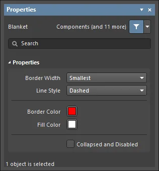 The Blanket dialog, on the left, and the Blanket mode of the Properties panel on the right
After placement, the Blanket dialog can be accessed by:
-
Double-clicking on the placed blanket object.
-
Placing the cursor over the blanket object, right-clicking then choosing Properties from the context menu.
During placement, the Blanket mode of the Properties panel can be accessed by pressing the Tab key. Once the blanket is placed, all options appear.
After placement, the Blanket mode of the Properties panel can be accessed in one of the following ways:
-
If the Properties panel is already active, by selecting the blanket object.
-
After selecting the blanket object, select the Properties panel from the Panels button in the bottom right section of the design space or by select View » Panels » Properties from the main menu.
The Blanket properties can be accessed prior to entering placement mode from the
Schematic – Defaults page of the Preferences dialog. This allows the default properties for the Blanket object to be changed, which will be applied when placing subsequent Blankets.
If the
Double Click Runs Interactive Properties option is enabled (default) on the
Schematic – Graphical Editing page of the
Preferences dialog, when the primitive is double-clicked or you right-click on a selected primitive then choose
Properties, the
Properties panel will open. When the
Double Click Runs Interactive Properties option is disabled, the dialog will open.
While the options are the same in the dialog and the panel, the order and placement of the options may differ slightly.
Editing Multiple Objects
The Properties panel supports multiple object editing, where the property settings that are identical in all currently selected objects may be modified. When multiples of the same object type are selected manually, via the Find Similar Objects dialog or through a Filter or List panel, a Properties panel field entry that is not shown as an asterisk (*) may be edited for all selected objects.
Editing via a List Panel
Panel pages: List Panels, SCH Filter
A List panel displays design object types from one or more documents in tabular format, enabling quick inspection and modification of object attributes. Used in conjunction with appropriate filtering – by selecting object types (using the panel's Include options), or by using the applicable Filter panel or the Find Similar Objects dialog – it enables the display of just those objects falling under the scope of the active filter. The properties for the listed objects may then be edited directly in the List panel.
Filtering Support
Two particularly useful keywords are available for use when targeting Blanket objects using logical query expressions. These complement the range of other keywords used to target a Blanket based on its properties.
-
Collapsed – the object is collapsed (also useful when targeting Compile Masks). This keyword can be found in the SCH Functions - Fields category when using the Query Helper.
-
IsBlanket – tests if the object is a Blanket. This keyword can be found in the SCH Functions - Object Type Checks category when using the Query Helper.
Create logical expressions for queries to target and return Blankets in your design as required. Some examples of logical query expressions targeting Blankets are:
IsBlanket And Collapsed – targets all Blanket objects that are currently collapsed.
IsBlanket And Not Collapsed – targets all Blanket objects that are currently not collapsed.
Disabling a Blanket
Once placed, Blankets can be temporarily disabled by clicking on the small triangle in the upper left ( ). Click once to disable and hide the Blanket; click again to re-enable it. This provides a convenient way of controlling the impact of the Blanket without needing to remove it completely from the design.
A Blanket can also be disabled by enabling the
Collapsed and Disabled option in the
Properties panel or the
Collapsed option when editing via the
SCH List panel.
Blanket Properties
Schematic Editor object properties are definable options that specify the visual style, content and behavior of the placed object. The property settings for each type of object are defined in two different ways:
-
Pre-placement settings – most Blanket object properties, or those that can logically be pre-defined, are available as editable default settings on the Schematic - Defaults page of the Preferences dialog (access from the button at the top-right of the design space). Select the object in the Primitive List to reveal its options on the right.
-
Post-placement settings – all Blanket object properties are available for editing in the Blanket dialog and the Properties panel when a placed Blanket is selected in the design space.
If the
Double Click Runs Interactive Properties option is disabled (default) on the
Schematic - Graphical Editing page of the
Preferences dialog, when the primitive is double-clicked or you right-click on a selected primitive then choose
Properties, the dialog will open. When the
Double Click Runs Interactive Properties option is enabled, the
Properties panel will open.
While the options are the same in the dialog and the panel, the order and placement of the options may differ slightly.
In the below options listing, options that are not available as default settings in the Preferences dialog are noted as "Properties panel only".
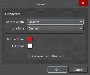
Properties
-
Border Width - use the drop-down to select the desired border width.
-
Line Style - use the drop-down to select the desired line style.
-
Border Color - click the color box to select the desired color for the border.
-
Fill Color - click the color box to select the desired color for the fill.
-
Collapsed and Disabled - check to collapse and disable blankets.
Indirect (Parameter-based) Directives
Parameter Set directives are necessary when targeting design objects in the Schematic that can't contain parameters, but for those objects that can, design directives can be applied indirectly by adding (and defining) them as parameters to the relevant schematic object. In essence, they are parameter-based directives.
Examples of how parameter-based directives could be used would include limiting the height of a particular component or adding a clearance constraint targeting all objects in the design. The required parameter that defines the constraint is added to the object as a rule.
When synchronized with the PCB, parameter-based directives that have been added to objects in the schematic will become PCB design rules. The scope of the corresponding PCB design rule will be determined by the nature of the object to which the parameter was first assigned. The following table summarizes the schematic parameter-to-PCB rule scope options that are supported.
In each case, the method of adding a rule-based parameter is the same. From the respective tab or dialog, perform the following:
-
Add a parameter as a rule.
-
Select which rule type to use.
-
Configure the constraints for the chosen rule type.
When adding design rule parameters to objects on a schematic, a unique ID is given to each rule parameter. The same IDs are given to the corresponding design rules that are created on the PCB. With this Unique ID, the constraints of a rule can be edited on either the schematic or PCB side, and the changes pushed through upon synchronization.
Specifying Component Classes
In a similar vein, component classes can be defined on the schematic by adding a ClassName parameter to targeted components and setting its value to the desired class name. When the design is transferred to the PCB, the defined component classes will be created.
To ensure Schematic defined Component Classes are propagated to the PCB, the following options must be set in the Project Options dialog:
-
Enable the Generate Component Classes option located in the User-Defined Classes region of the dialog's Class Generation tab.
-
On the dialog's Comparator tab, set the Differences Associated with Components » Extra Component Classes Mode setting to
Find Differences.
The above-listed Class Generation tab option is displayed in the image below. Hover over the image to view the Comparator tab option setting.

To propagate Component Classes to the PCB, enable the Generate Component Classes option on the Class Generation tab. Hover over the image to show the Comparator tab where you will need to set the Extra Component Classes Mode setting to Find Differences.
Once defined, classes may be locked in the Properties region of the Properties panel of the respective component properties.
In the PCB editor, a component can belong to multiple Component Classes. To define this in the schematic, separate each PCB Component Class name with a comma in the schematic component parameter value (show image![]() ).
).
Controlling the Printing of Directives
By default, all design directives are included in the printing of the schematic sheets. This can, however, be changed:

Control the printing of directives as required. For No ERC directives, you can opt to print certain symbol styles, while excluding others.

