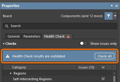
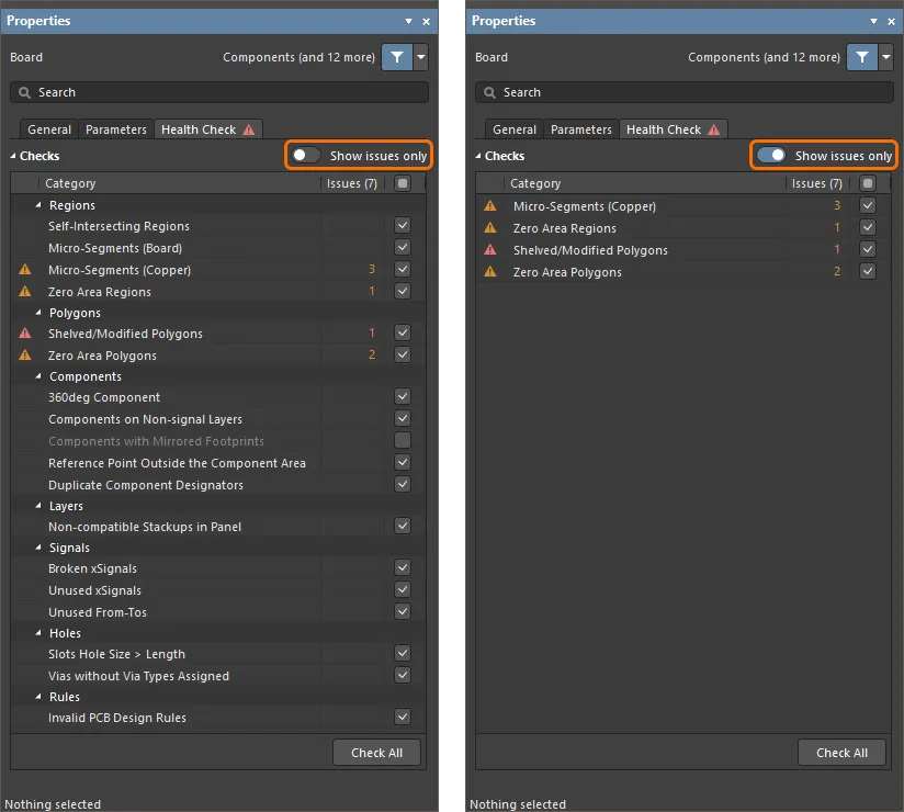
PCB Health Check Monitor
The final goal of each PCB design is to get a correct and reliable set of assembly and fabrication outputs, and the purpose of any design tool is to provide a user with tools to find and resolve the issues that could arise during the design process before the design goes to production. During its constant development, Altium Designer delivers enhancements and bug fixes in each release to provide you with a better design experience and to help you avoid some “unhealthy” layout aspects of your PCBs. In some cases, such areas of a board might be fine from the perspective of Altium Designer’s DRC system, not leading to serious fabrication issues. However, they could result in software performance degradation and issues during MCAD co-design or generation of PCB outputs. For example, PCB components could have 360 degrees rotation value in previous versions of Altium Designer, but this situation is not allowed anymore in the current versions – the software will set such components to 0 degrees.
These “unhealthy” board layout elements may be present in designs created in versions of the software before it was improved and fixed in certain areas. The PCB Health Checks functionality is available to help you detect and resolve such issues and other issues that can arise under certain conditions. These checks allow you to discover common issues in the PCB design, fix them, and avoid potential problems during the next stages of the design and manufacturing process.
When no object is selected in the active PCB document, the Properties panel includes the Health Check tab that enables you to configure, perform, and explore the results of the PCB Health Check.
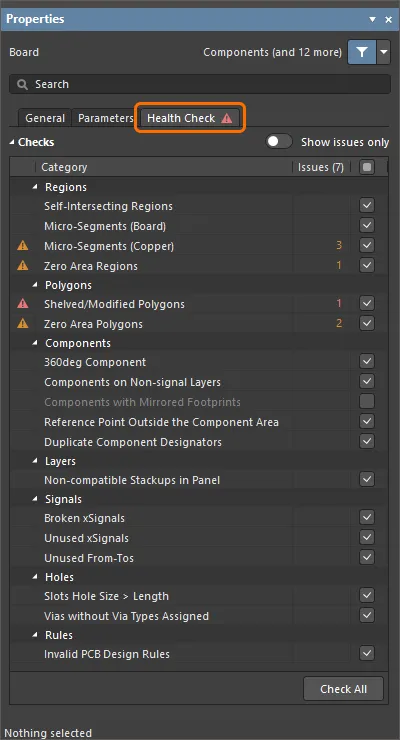
The interface to the Health Check Monitor is the Health Check tab of the Properties panel when no object is selected in the PCB document.
Setting Up and Running a Health Check
Available checks are listed in the grid area of the Checks region on the Health Checks tab. All checks are grouped by relevant categories (Regions, Polygons, Components, etc.). Using the checkbox column, you can enable/disable specific checks or use the checkbox in the column header to enable/disable all checks.
A health check is performed automatically when the PCB document is opened. Anytime during the design process, you can run a specific check manually by right-clicking it in the list and selecting the Run Check command or run all enabled checks by clicking the Check All button at the bottom of the list.
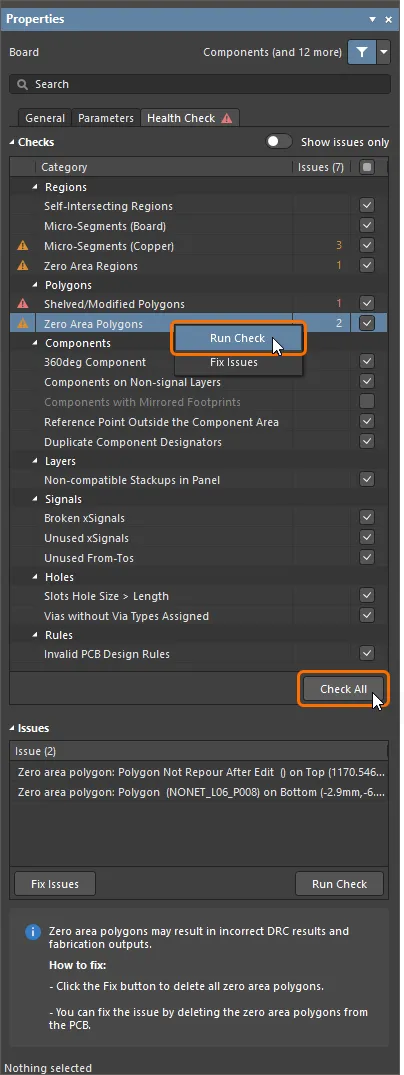
Run a specific check or run all checks at once.
If issues are detected for a check, the number of the issues detected for this check will be shown in the Issues column. The total number of issues found for the current PCB design is shown in parentheses in the column header. Also, an icon will be shown in this column. The icon reflects the severity level of the found issue, depending on its type:
-
 – Info
-
 – Warning
-
 – Error
The icon of the most severe issue detected will also be shown next to the Health Check tab title. If there are no issues, the ![]() icon will be shown in the tab title.
icon will be shown in the tab title.
Select a check entry to show the list of issues detected for this check in the Issues region of the panel.
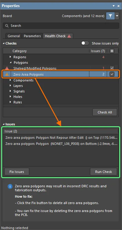
Select a check to show the list of detected issues.
Resolving the Detected Issues
When clicking a check in the Check region of the panel, the panel's Issues region will be populated with the issues detected for this check. Click an issue in the list to zoom, center, and highlight (where possible) an offending object in the PCB editor's design space. Recommendations on how an issue for the selected check can be fixed are shown in the info region of the panel.
The following checks can be fixed automatically:
-
Zero Area Regions
-
Zero Area Polygons
-
Micro-Segments
-
Shelved/Modified Polygons
-
360deg Component
-
Components with Mirrored Footprints
-
Duplicate Component Designators
-
Unused xSignals
-
Unused From-Tos
To use the automatic fix, select a check in the list and click the Fix Issues button at the bottom of the issue list. Alternatively, right-click a check in the Checks list and select the Fix Issues command from the menu that appears.
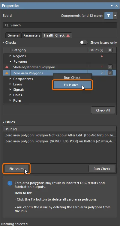
Fix the detected issues automatically using the Fix Issues command.
Performing a Health Check during Output Generation
When trying to generate the outputs from an OutJob file or directly from the PCB editor and the design contains a critical issue (a shelved polygon or a polygon that has been modified but not repoured and/or a panel that has a layer stack non-compatible with the layer stack of the parent board), a warning dialog will be displayed. The dialog shows you a warning that outputs to be generated will not be correct and the number(s) of offending objects. You can cancel output generation and open the Health Check tab right from the dialog or proceed with output generation. For the non-compatible layer stack issue, you can also open the compatibility HTML report.
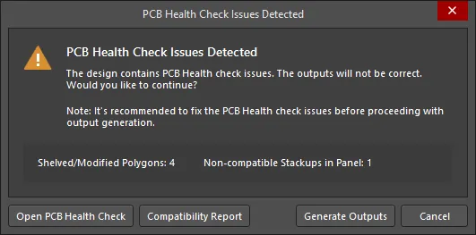
The PCB Health Check Issues Detected dialog
Reporting the Detected Issues
Issues detected by the PCB Health Check Monitor can be listed in the HTML report generated when performing a Batch DRC. In the Design Rule Checker dialog, select the Create Report File option and its Report PCB Health Issues sub-option.
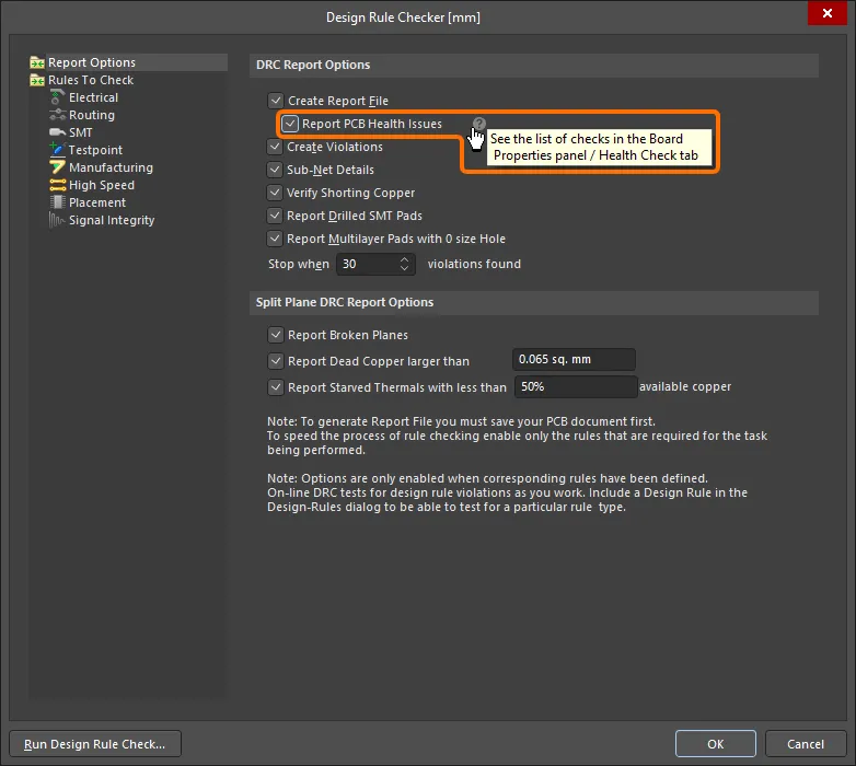
The Report PCB Health Issues option in the Design Rule Checker dialog
After running the Batch DRC using the dialog's Run Design Rule Check button, the number of detected PCB Health Issues will be shown at the top of the report, and the issues will be listed under the PCB Health Issues heading.
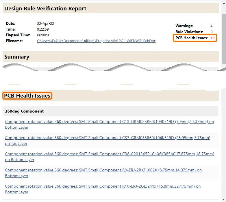
An example of the generated report when the Report PCB Health Issues option was enabled in the Design Rule Checker dialog

