
Interrogating & Resolving Design Violations
Altium Essentials: PCB Design Rule Checks
This content is part of the official Altium Professional Training Program. For full courses, materials and certification, visit Altium Training.
With care and attention and staged design rule checking along the way, running that final Batch DRC on the finished, fully routed board takes the design one step closer to release.
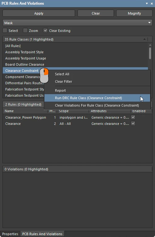
 DRC reports can appear daunting to the new PCB designer. The secret to keeping the process manageable is to develop a strategy. One strategy is to limit the number of violations reported by setting a limit in the Design Rule Checker dialog. Another strategy is to run the DRC in a number of stages, enabling the rules in blocks in the DRC dialog, and a third is to run selected rules individually from the PCB Rules and Violations panel. With experience, you will develop a preferred approach to testing the various design rules.
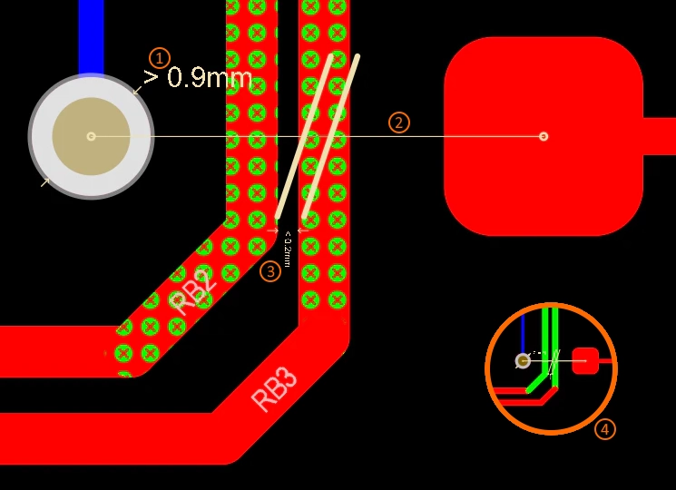
The DRC system supports two styles of flagging, or marking, objects that are violating a design rule; by adding a violation overlay onto the object, or by placing a violation detail marker adjacent to the object.
For example, in the image number 1) shows a violation detail marker flagging a via with a diameter greater than the 0.9mm allowed by the applicable Routing Via Style design rule. Number 2) is also a detail marker – a line drawn from the via to the pad broken by a double-slash, indicating the location of an Un-Routed Net. Number 3) is both a clearance detail marker flagging a Clearance violation (clearance is less than 0.2mm), as well as a violation overlay (green dots) flagging the primitives involved in this violation. 4) shows the same view zoomed out, note how the violation overlays are very effective at locating violating primitives at low zoom levels.
Features for Highlighting a Violation as you Browse
To effectively resolve a design violation, you must first be able to locate it. The PCB editor provides various methods for browsing and interrogating design violations, including: the Messages panel, the PCB Rules and Violations panel, the DRC report, and even from outside of Altium Designer when you are viewing the project in the Altium Web Viewer.
The PCB editor also includes features to present and highlight a violation as you browse using one of these methods. Underlying the PCB editor is a powerful query engine, coupled to flexible zooming and highlighting features. The query engine can quickly filter the large volume of design data, returning exactly the object(s) of interest. Those objects can then be highlighted in the design space using selection, zooming, and masking or dimming.
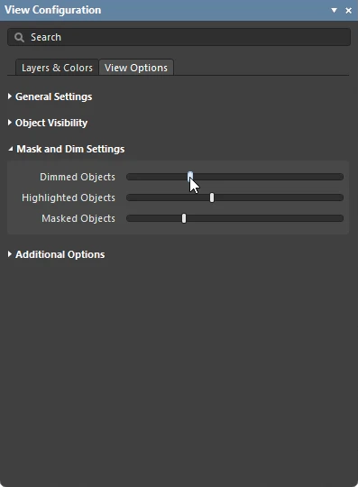
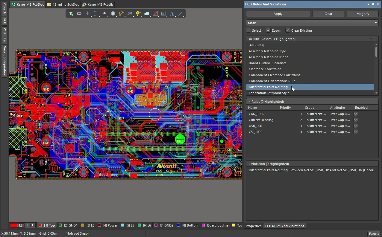
When you click on a violation entry the PCB editor applies filtering using the offending object(s) as the scope of the filter. The view in the main design window updates, depending on how the highlighting options are configured at the top of the panel (Mask/Dim/Normal, Select, Zoom). If zoom is enabled, then the violation is centered in the display. Learn more about masking and diming, and the query engine and filtering system.
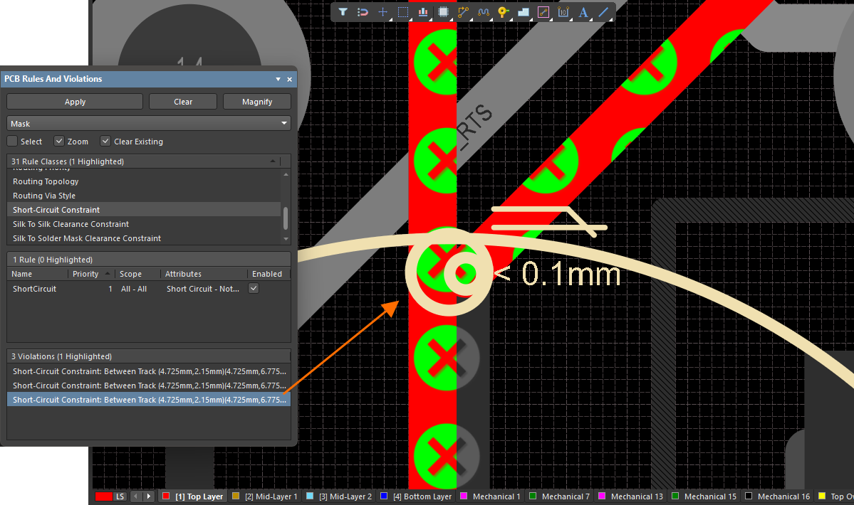
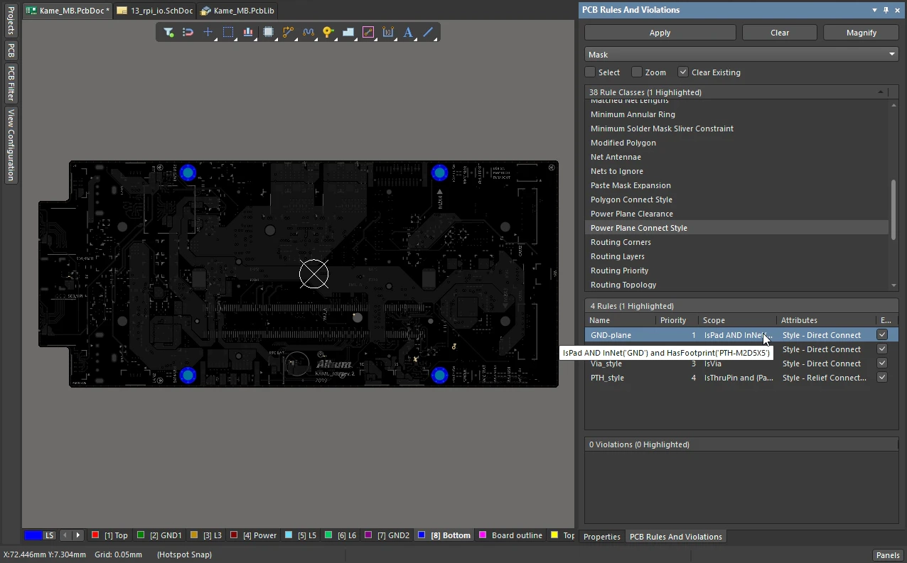
Interrogate rule violations using the PCB Rules And Violations panel, click on an entry to highlight it as per the settings at the top of the panel.
PCB Rules and Violations Panel
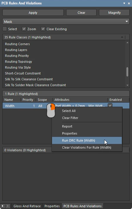
The PCB Rules And Violations panel is purpose-built for managing design rules and examining violations in the board design space. The panel provides a central point for browsing and editing rules, instigating design rules checks, and viewing individual violations in the editor design space.
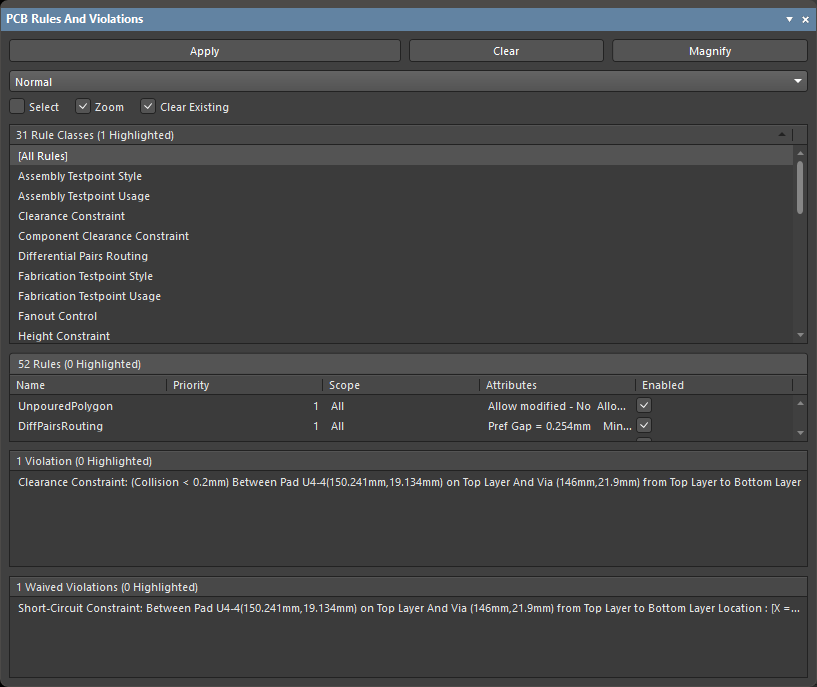
The PCB Rules And Violations panel
PCB Rules And Violations panel |
|
| Accessing the panel | To display the PCB Rules And Violations panel:
|
Highlighting Controls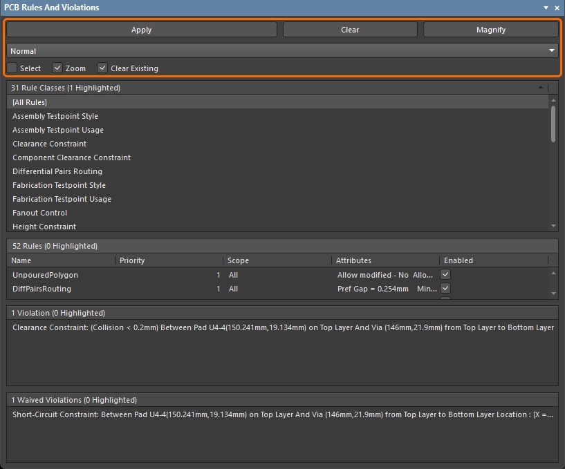 |
Use these controls at the top of the panel to configure the response as you click on entries in the panel sections below:
|
Rule Classes section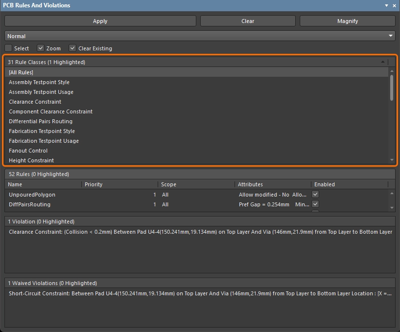 |
This section of the panel lists all of the Rule Classes (rule-types that one or more design rules has been defined for). In this section of the panel:
|
Rules section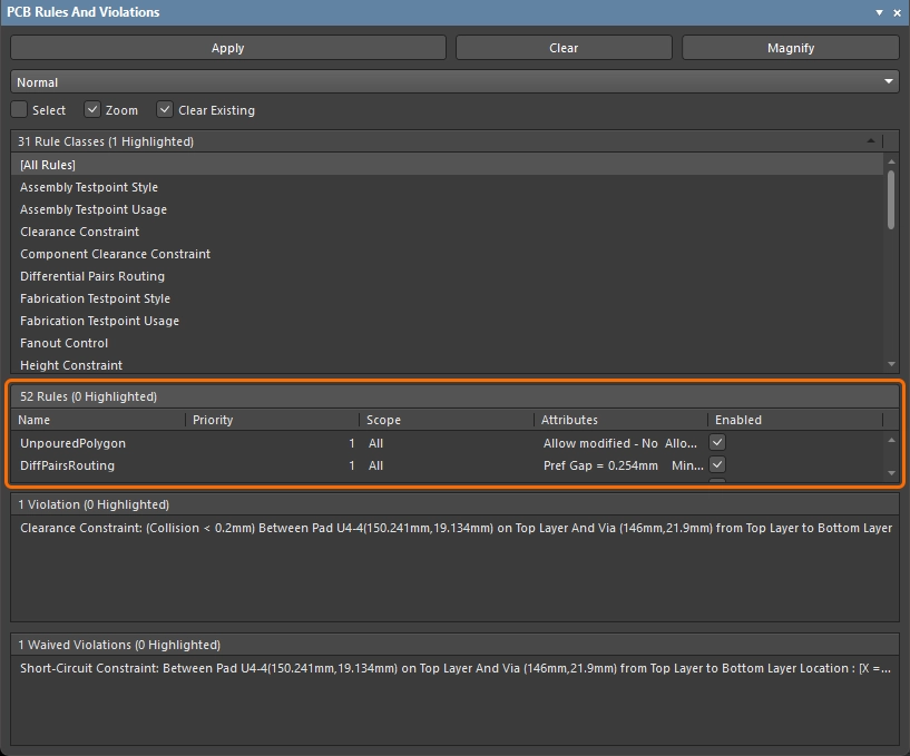 |
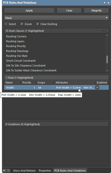
This section of the panel lists the individual design rules defined for the currently selected Rule Class.
|
Violations section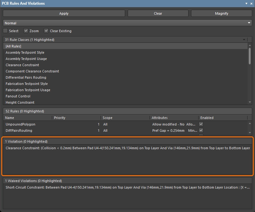 |
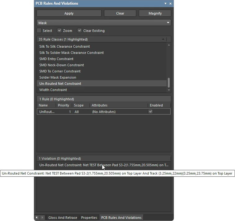
This section of the panel details each rule violation reported by the last design rule check.
|
Waived Violations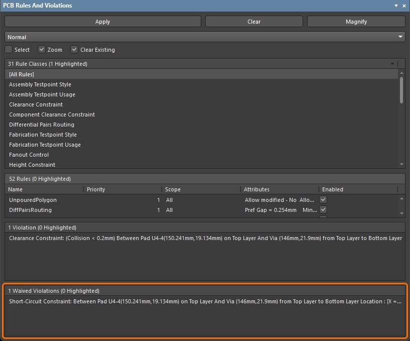 |
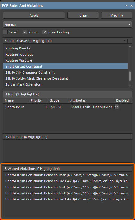
This section of the panel details each rule violation that is waived, as reported by the last design rule check.
|
 )
) ).
). ).
). ).
). )
) ).
). ).
). ).
). ).
). ).
).Working with Violations in the Design Space
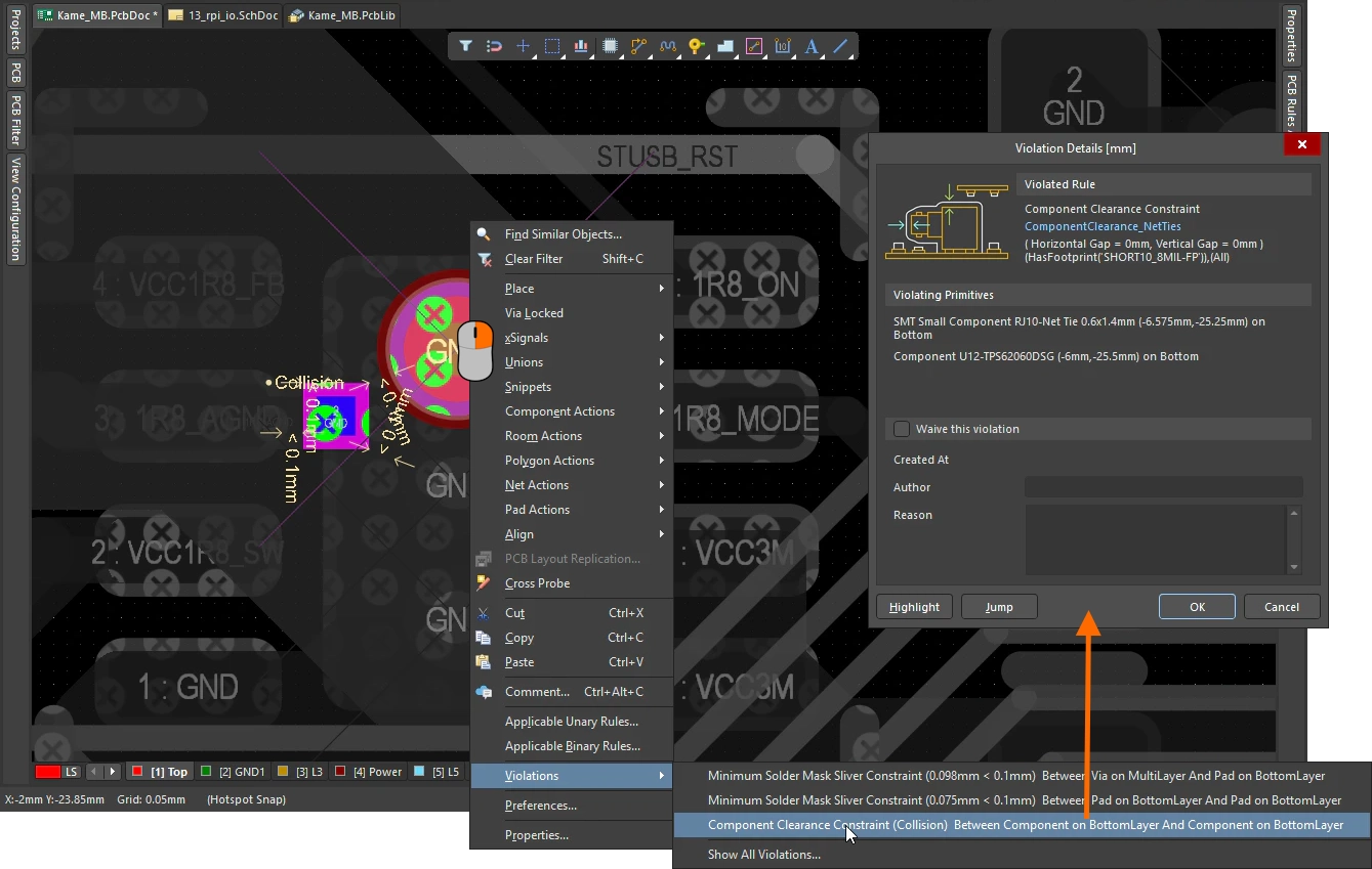
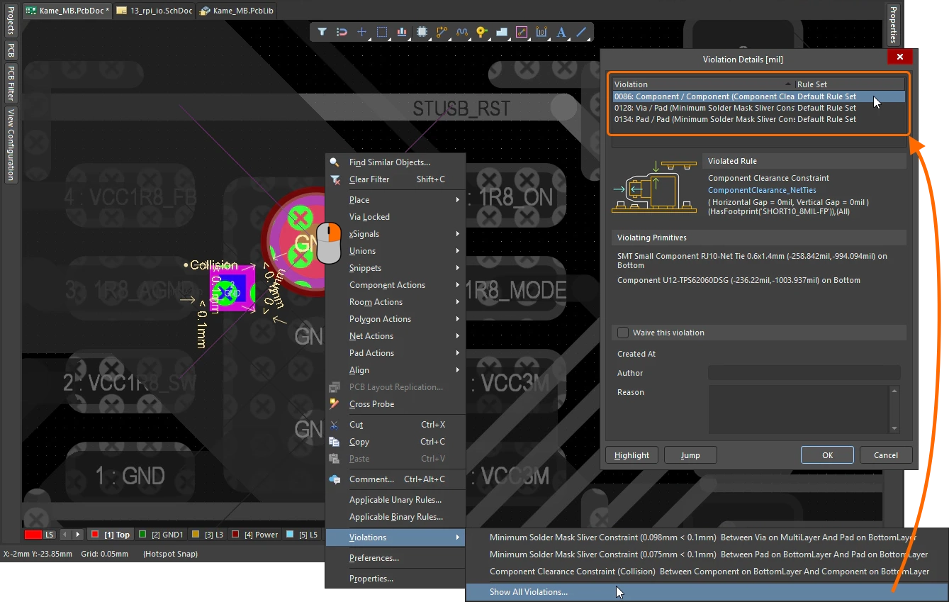
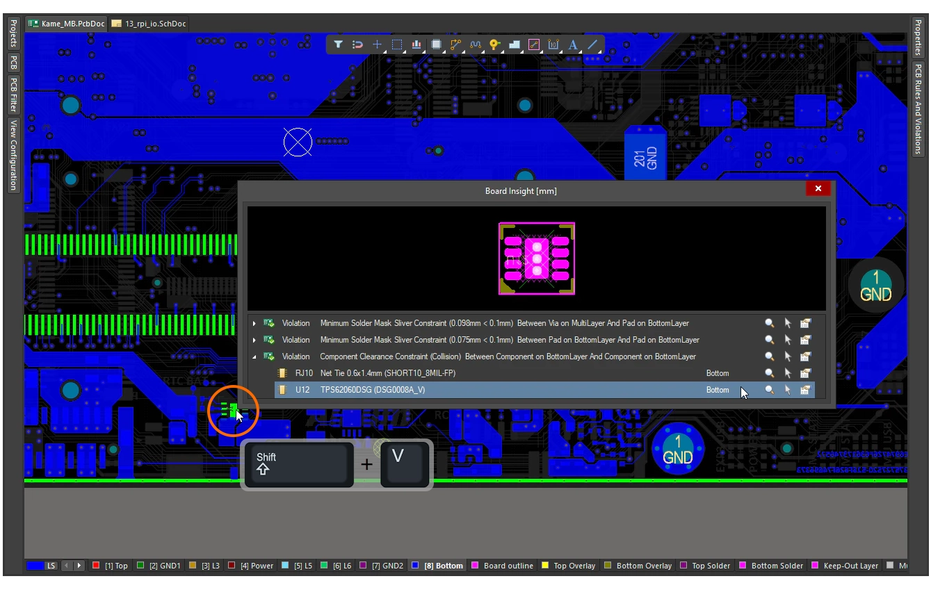
Violations can also be interrogated directly in the PCB design space. Position the cursor over the offending object, right-click, and choose a command from the Violations sub-menu, as shown in the first two slides below. Alternatively, use the Board Insight panel (slide 3).
Examining a Violation in the Design Space |
|
| Inspect a violating object | When you right-click on a violating object the context menu will include a Violations submenu. This submenu includes an entry for each rule that is in violation as well as a Show All Violations option. |
| Violation details | When an entry in the Violations submenu is chosen, the Violations Details dialog opens. Towards the top of the dialog are the details of the rule that is in violation. The pale blue rule name is a link, click on it to open the PCB Rules and Constraint Editor, where the rule settings can be examined and edited. The next section of the dialog details the primitive(s) in violation, and below that are options for Waiving (choosing to ignore) this violation. More about the Violations Details dialog. More about waiving a violation. |
| Showing all violations | Select the last entry in the Violations submenu to Show All Violations. This command also opens the Violations Details dialog, except this time it includes a list of all violations that were present under the cursor when you performed the right-click (as shown in the second slide above). This list allows you to examine the details of each of the violations. More about the Violations Details dialog. |
| How the display responds | When you choose an entry from the Violations submenu, as well as the Violation Details dialog opening, the display zooms into the object(s) detailed in the dialog. This zoom level is fixed. |
| Other dialog options | The default behavior is to jump and zoom to the violation. The Jump button can then be used if you open the dialog using the Show All Violations command and want to jump to each of the listed violations in turn. The Highlight button temporarily dims all objects that are not part of the violation, move the dialog to one side to more easily see the impact of this. |
| Board Insight panel | An alternate approach is to examine the violations in the Board Insight panel. When the cursor is over a violating object, press Shift+V to display the panel, where each violation can be jumped to, selected, and the properties examined in the Violation Details dialog. Click anywhere in the design space to close the panel. Note that the panel will not appear when you press Shift+V if there is no violation under the cursor when the shortcut is pressed. |
| From the Messages panel | If there are violations detected during a Batch DRC, the Messages panel will automatically open. Double-click on a violation in the panel to zoom to the object(s) causing that violation ( ). The violating object(s) will be zoomed and centered, but no other highlighting (masking, dimming) will be applied. The zoom level is configured in the System – Navigation page of the Preferences dialog ( ). The violating object(s) will be zoomed and centered, but no other highlighting (masking, dimming) will be applied. The zoom level is configured in the System – Navigation page of the Preferences dialog (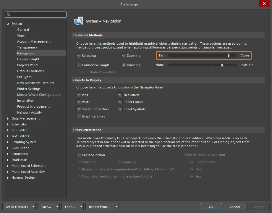 ), or by clicking the Magnify button at the top of the PCB Rules and Violations panel ( ), or by clicking the Magnify button at the top of the PCB Rules and Violations panel (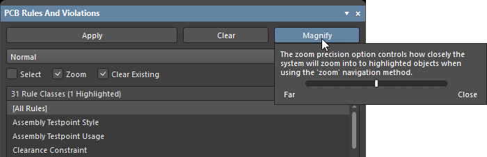 ). ). |
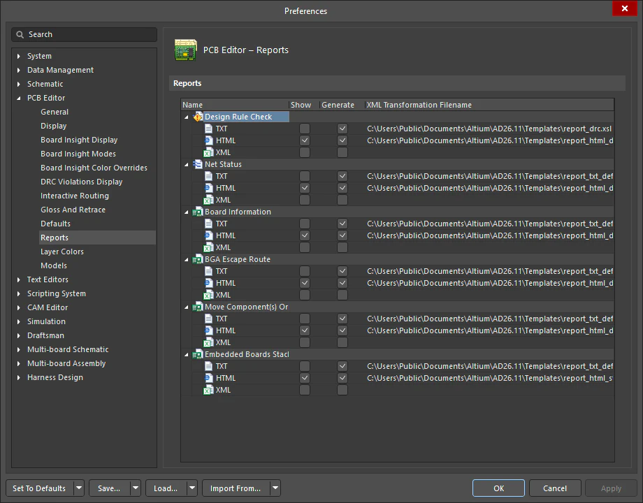
| From a DRC report | If the option to Create Report File is enabled in the Design Rule Checker dialog, violations detected upon running a Batch DRC will be listed in a generated Design Rule Verification Report. Click on the hyperlinked entry for an offending object to cross-probe directly to that object in the design space ( |
 ).
). ).
).Violations Details Dialog
 The dialog details the violation currently being examined.
| Violated Rule | The design rule that is being violated, for the violation entry currently being examined. The rule is displayed in terms of its type, violated constraint(s), and scoping. The rule name is a live link, click on the link to open the PCB Rules and Constraints Editor, where the rule settings can be changed. If the PCB includes a user-defined rule set and the violating rule is in that set, the name of the rule set is also displayed. This feature is in Open Beta and available when the |
| Violating Primitives | this area presents the primitives involved in the currently selected violation, in terms of object type, identifier (where applicable), location, and layer upon which they reside. |
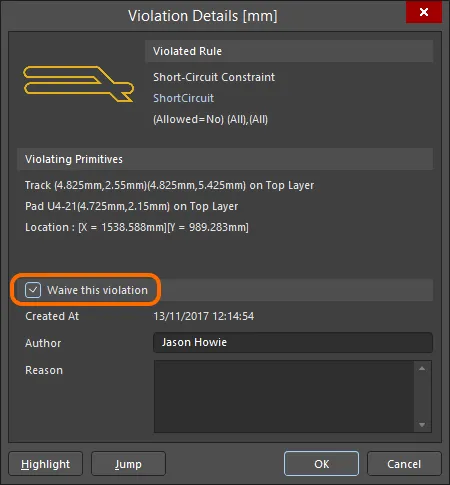
| Waive this violation | Enable the checkbox to waive the violation, completing the following details:
|
| Highlight | When this button is clicked the violating primitives detailed in the dialog are momentarily highlighted in the design space. Highlighting essentially leaves the offending primitives in their normal visibility with all other objects in the design space becoming temporarily monochromatic. This button does not center the violation, click Jump to do that. Note that it can help to move the dialog away from the center of the monitor to more easily see the highlighted primitives, before clicking Highlight. |
| Jump | When this button is clicked the violating primitives detailed in the dialog are centered in the design space. The primitives will effectively be zoomed and centered within the design space. |
Interpreting the Violations
A screen peppered with violation markers can seem daunting. You can help this by managing the process in a staged way, for example holding off the manufacturing rule checks until component placement and routing is complete.
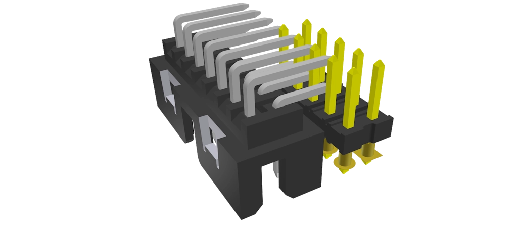
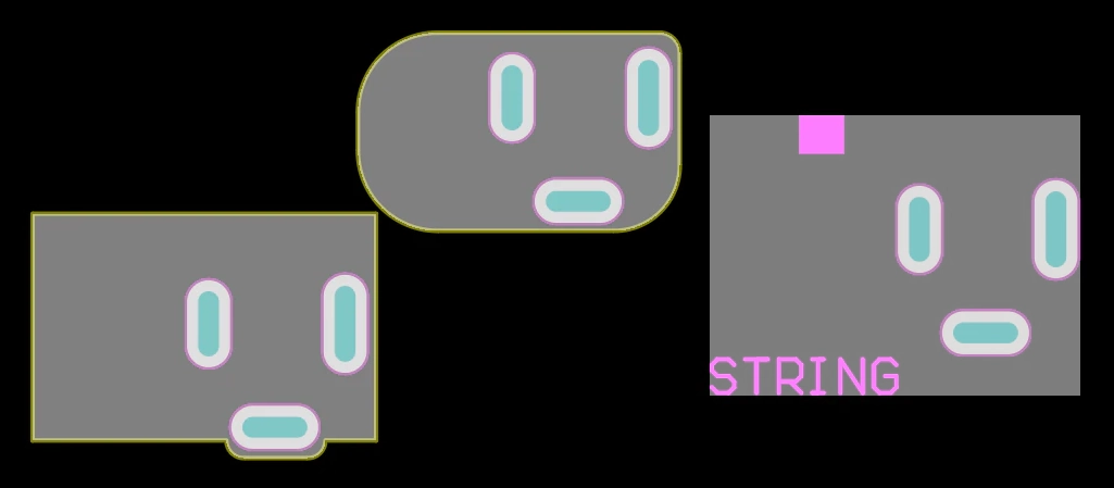
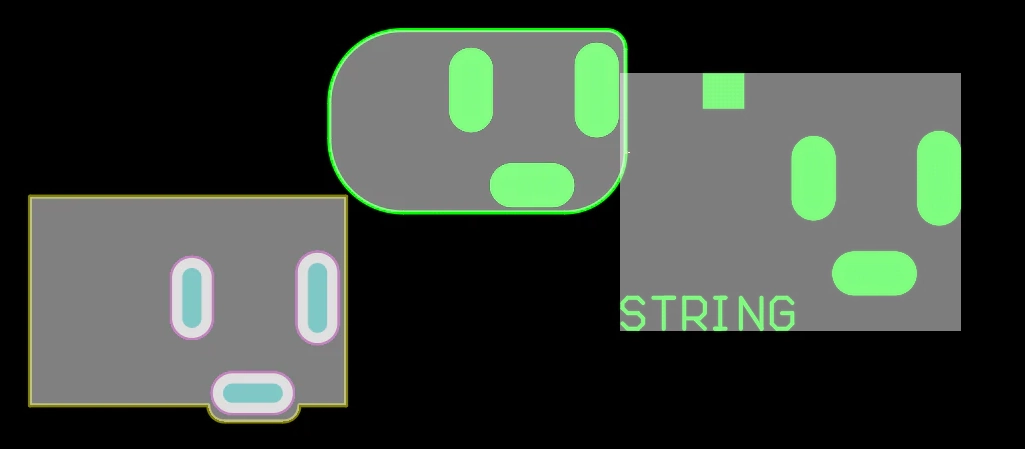
The DRC system supports both 2-dimensional and 3-dimensional component clearance checking.
Tips for Interpreting Violations |
|
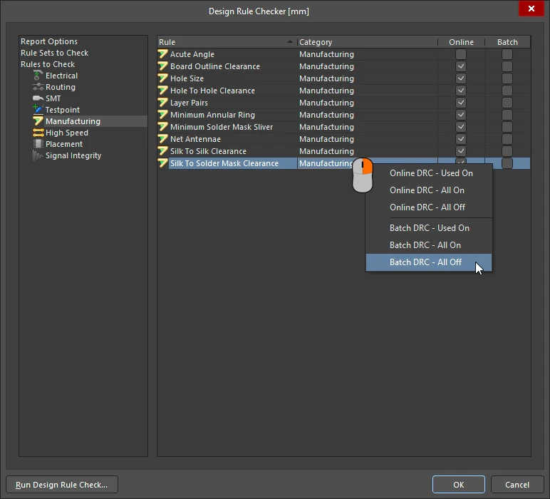
| Test in stages | A good approach is to only enable the rules for testing that relate to where you are in the design process – if you are placing components then enable the Placement rules and disable all others, if you are routing then enable just the Routing rules, and so on. Use the right-click context menu in the Design Rule Checker dialog to toggle rule checking on and off. A handy feature is that the context menu commands only apply to the rules that are currently visible, if you select a rule-type on the left then you can quickly toggle the rules of that type off or on ( |
| Use detail markers | The advantage of violation detail markers is that they give feedback about the type of violation, and where possible, details of the violation. |
| Understanding component collisions | To understand why a component collision is being flagged, it is important to understand how the DRC system views the components:
Learn more about the Component Clearance design rule. |
 ).
).Selectively Waiving DRC Violations
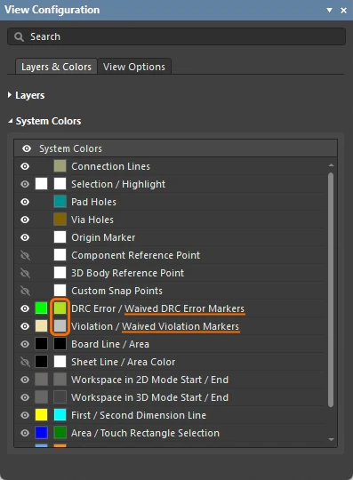
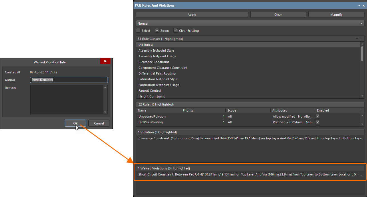
The software supports the ability to selectively waive any DRC violation. This allows you to effectively 'suppress' a violation that is considered not to be an issue, without having to craft a special (and perhaps complex) design rule to handle the design situation. Waved violations are detailed in the PCB Rules and Violation panel when their rule-type is selected.
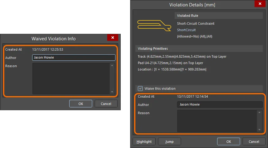 Information that is stored for a waived violation is entered either through the Waived Violation Info dialog or the Violation Details dialog.
Waiving DRC Violations |
|
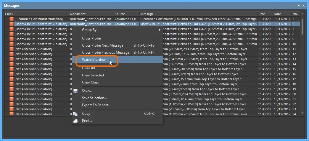
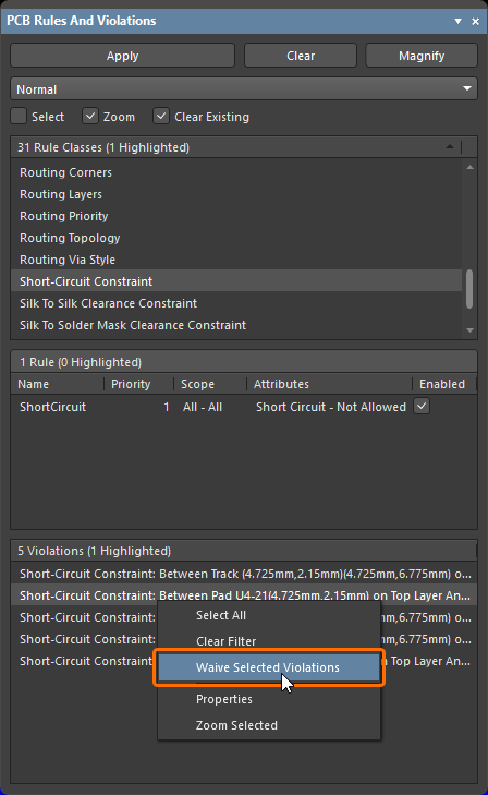
| Waiving a DRC Violation | DRC violations can be waived by:
|
| What information is stored | Against each waived violation, the software records three pieces of information:
|
| Working with Waived Violations |
|
| Revoking a waived violation | The waived status for a violation can be revoked at any time by:
|
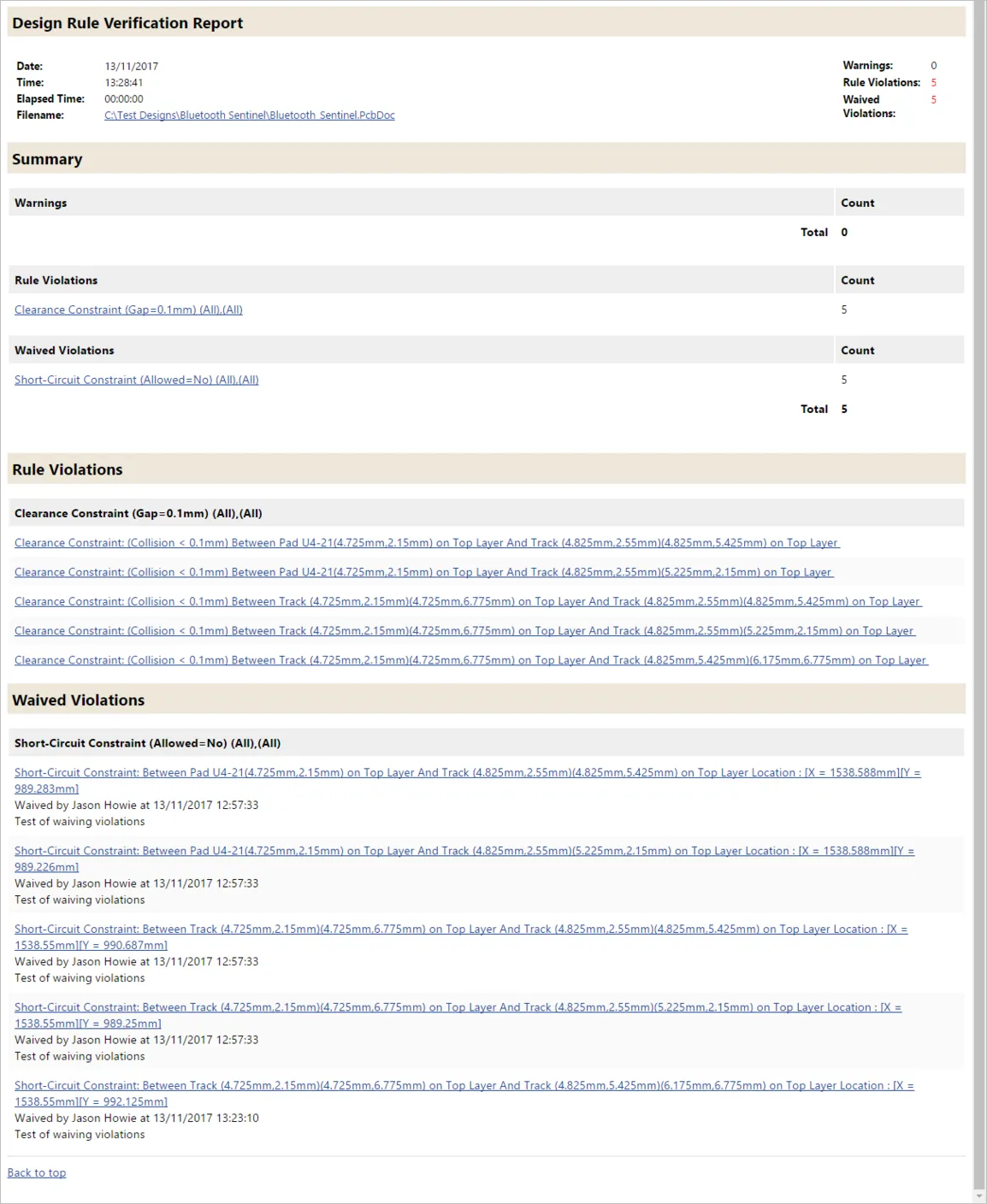
| Documenting Waived Violations | If the Create Report File option is enabled in the Design Rule Checker dialog, waived violations are included in a separate section of the report ( |
 ).
). ).
). ).
). ).
). ).
).