Tutorial - A Complete Design Walkthrough with Altium Designer


Welcome to the world of electronic product development in Altium's world-class electronic design software. This tutorial will help you get started by taking you through the entire process of designing a simple PCB - from idea to output files. If you are new to Altium software, it is worth reading the Exploring Altium Designer page to learn more about the interface, information on how to use panels, and an overview of managing design documents.

To learn more about a command, dialog, object or panel, press F1 when the cursor is over that item.


The Design

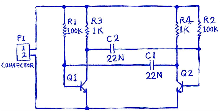
The design for which you will be creating the schematic and designing a printed circuit board (PCB) is a simple astable multivibrator. The circuit is shown below; it uses two general purpose NPN transistors configured as a self-running astable multivibrator.

Circuit for the multivibrator.

You're ready to begin capturing (drawing) the schematic. The first step is to create a PCB project.


Creating a New PCB Project

In Altium's electronic design software, a PCB project is the set of design documents (files) required to specify and manufacture a printed circuit board. The project file, for example, Multivibrator.PrjPCB is an ASCII file that lists the documents in the project as well as other project-level settings, such as the required electrical rule checks, project preferences, and project outputs, such as print and CAM settings.

A new project is created by running the File » New » Project command to open the Create Project dialog.

Create Project dialog

As well as Local Projects, The Create Project dialog can be used to create a Version Controlled project, or a managed project that is stored in a managed content server. Use the links to learn more about these types of projects.

A new project is created by running the File » New » Project command to open the Create Project dialog.

Create Project dialog

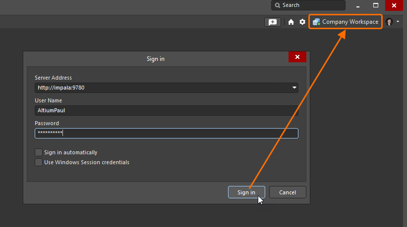
Altium NEXUS is built for collaborative design, with features that help keep the design team members in sync. A key ingredient to delivering these collaboration capabilities is the way that designs are managed - by storing them in a Managed Content Server. To complete this tutorial, you will need to be signed in to a Managed Content Server.

Connect to Server

Learn more about Collaborative Design
Learn more about Working with a Managed Content Server


Adding a Schematic to the Project

The next step is to add a new schematic sheet to the project.

Add a new schematic to the project

Add a schematic sheet to the project, name and save the schematic, and save the project.

When the blank schematic sheet opens, you will notice that the workspace changes. The menu bar includes new items and a bar with buttons becomes visible - you are now in the Schematic Editor. Each editor presents its own set of menus and panels and supports its own set of shortcut keys.

An entire set of floating panels can be closed using the Close panels button icon at the top right of the panel, and an individual panel can be closed by right-clicking on its name. When needed, a panel can be reopened via the  Panels button button at the bottom right of the application. Alternatively, press the F4 shortcut to hide/display all floating panels.


Setting the Document Options

Panel page: Schematic Document Options

Before you start drawing your circuit, it's good to set up the appropriate document options, including the Sheet Size, and the Snap and Visible grids.

Document options are configured for each schematic sheet, set the sheet size as required.

As well as the technique described in the collapsible section below, the Document Options properties can also be accessed by double-clicking in the sheet border.

Environment options, such as the cursor type, selection color and autopan behavior, are configured in the Preferences dialog (Tools » Preferences).


Accessing the Components

Related article: More about Components and Libraries

The real-world component that gets mounted on the board is represented as a schematic symbol during design capture, and as a PCB footprint for board design.

Components can be:

  • Placed directly from the Manufacturer Part Search panel. This panel gives you instant and up-to-date access to a powerful component search and aggregation system, detailing millions of components from thousands of manufacturers, each with real-time supply chain information. Many of the components are design-ready, complete with a symbol and a footprint model; these parts will include the  Has Models icon icon in the panel.
  • Created in and placed from local file libraries, or your company's Managed Content Server. These components are searched for and placed through the Components panel. More on this approach in the Working with Your Own Components section below.
  • Created in and placed from your company's Managed Content Server, these components are searched for and placed through the Components panel. 
    Learn more about managed components.
  • For this tutorial, all of the parts will be sourced from the Manufacturer Part Search panel.
  • Throughout the tutorial, the terms component and part are both used to describe the design components you will be placing and wiring.

Searching for New Parts

Main article: Manufacturer Part Search panel

Your go-to location to find new components is the Manufacturer Part Search panel. To open the Manufacturer Part Search panel, click the Panels button button at the bottom right of the application and select Manufacturer Part Search from the menu. Panels that are currently visible are marked with a check in the menu.

The first time the Manufacturer Part Search panel is opened, it will display a list of component categories as shown below.

The Manufacturer Part Search panel, before performing a search.

Utilizing Altium Designer's advanced component search engine, the Manufacturer Part Search panel can be used in a straightforward search mode by entering a query in the main Search field, or in its advanced faceted mode by progressively refining the search criteria using the Categories and Filters choices – or by using both capabilities together.

  • To perform a straightforward search, type a search description into the Search field at the top of the panel.

For example: LED green clear 0603 SMD

Manufacturer Parts Search panel, simple search
Use the Search field to perform a text-based search. Click the small x next to the search string to clear it, click the search string to reload it into the Search field for editing.

  • Or to perform a faceted search, use the Categories and Filters to explore potential parts by toggling criteria on and off.

For example:

  1. First select a Category, such as LEDs,
  2. then Filter the LEDs category by the Color, Case/Package, Mount, Has Model, and so on.

Or use a combination of the Categories, Filters, and the Search field to perform a faceted search.

Panels and dialogs that support searching for components have a landscape mode and a portrait mode. As the panel/dialog is resized the controls will re-arrange, so they may not present exactly as they are shown and described here.

Exploring the Search Results

The search results region of the panel displays a list of manufacturer parts that wholly or partly match the search criteria. Click on a part to select it and display a link giving access to up-to-date supply chain information about that part.

Manufacturer Parts Search panel, details of the selected part

Understanding the Supplier Tile

There is a large amount of information presented in each SPN tile. Hover the cursor over an icon or detail to display a tooltip with more information.

The SPN tile includes detailed information about the part and its availability. The SPN tile includes detailed information about the part and its availability.


Working with your own Components

At some point, you will need to create your own components and store them locally. There are essentially two types of components that can be created:

  • Managed components - components are created and stored in a Managed Content Server.
    Learn more about managed components
  • Unmanaged components - components are created and stored in Altium-format library files. These are referred to as file-based libraries or file libraries.
    Learn more about file-based components and libraries

Both managed and unmanaged components are browsed, searched for and placed in the Components panel. Like the Manufacturer Part Search panel, the Components panel supports string-based searching, faceted searching, or a combination of both. Use the  Panels button button to display the Components panel.

 The Components panel being used to browse components stored in a managed content server; hover to show the panel being used to browse file-based components.

In this tutorial, all of the components will be placed from the Manufacturer Part Search panel. The information in this section is included to give you a basic overview of how to work with unmanaged components.


Placing from the Manufacturer Part Search Panel onto the Schematic

If a component that you have found in the Manufacturer Part Search panel has Altium design models, it will display the  Has Model icon icon. If a component has models, the schematic symbol and footprint models will be listed in the Details region of the panel (click the  Manufacturer Part Search panel, part information button in the panel to display this region). This component can be placed directly from the panel onto the current schematic sheet.

Use the faceted search features in the Manufacturer Part Search panel to only display components with models.Use the faceted search features in the Manufacturer Part Search panel to only display components with models.

The Filters region of the panel includes a Has Model filter. Enable this to only display design-ready parts. Click Manufacturer Part Search panel, Filters button to display the available filters.

To place a component from the panel, you can:

  • Select Place from the Download button - the cursor automatically moves to be within the bounds of the schematic sheet and the component appears floating on the cursor; position it and click to place. After placing a component, another instance of the same component will appear on the cursor; right-click to drop out of placement mode.
  • Right-click on the component and select Place from the context menu. The component appears floating on the cursor; position it and click to place. Note that if the panel is floating over the workspace, it will fade to allow you to see the schematic and place the component. After placing a component, another instance of the same component will appear on the cursor; right-click to drop out of placement mode.
  • Click and drag - click and drag the component from the grid region of the panel onto this sheet. This mode requires that the cursor is held down; the component is placed when the cursor is released. Using this technique only one component is placed. After placing the component, you are free to select another component or another command.

Placement Tips

While the component is floating on the cursor, you can:

  • Press Spacebar to rotate it counterclockwise in 90 degree increments.
  • Press X to flip it along the X-axis; press Y to flip it along the Y-axis.
  • Press Tab to display the Properties panel and edit the properties of an object prior to placement. The values entered become the defaults. If the designator has the same prefix, it will be auto-incremented.
  • During component placement, the software will automatically pan if you touch the window edge. Autopanning is configured in the Schematic - Graphical Editing page of the Preferences dialog. If you accidentally pan beyond where you want, while the component is floating on the cursor you can:
    • Ctrl+Wheel Roll to zoom out and in again, or
    • right-click and drag to slide the schematic around, or
    • Ctrl+PgDn to display the entire sheet again.
  • If the Manufacturer Part Search panel is floating over the schematic sheet when you place a part, it will automatically become transparent whenever the cursor+component gets close to it. The transparency of floating panels is configured in the System - Transparency page of the Preferences dialog. Alternatively, all floating panels can be hidden/displayed at any time (while running a command or not) by pressing the F4 shortcut.

►? Learn more about Schematic Placement and Editing Techniques

Working with the Properties panel during Placement

During object placement, if you press Tab the editing process will pause and the interactive Properties panel will open. The default behavior is for the most commonly edited field to be highlighted, ready for editing. Because the editing process is paused, you can use the cursor (or press Tab on the keyboard) to move to another field in the panel.

When you have finished editing, click the Pause button ( Pause button ) as shown in the image below to return to object placement. Alternatively, press Enter to finish object editing and return to object placement.

Editing is paused when you press Tab during placement - click the Pause icon on the screen to return to placing the component.

Editing is paused when you press Tab during placement - click the Pause icon on the screen to return to placing the component.


Placing the Multivibrator Parts

Now, it is time to use the Manufacturer Part Search panel to find the components needed for the Multivibrator circuit as listed in the following table.

Designator Description Comments
Q1, Q2 General purpose NPN transistor, eg BC547 or 2N3904 Search for: transistor BC547, chose BC547CG
R1, R2 100K resistor, 5%, 0805 Search for: resistor 100K 5% 0805
R3, R4 1K resistor, 5%, 0805 Search for: resistor 1K 5% 0805
C1, C2 22nF capacitor, 5%, 16V, 0603 Search for: capacitor 22nF 16V 0603
P1 2-pin header, thruhole Use the faceted search feature to filter for a: Connector, 2-pin, vertical, male, header

Once you have placed the components, the schematic should look like the image below.

You can proceed to find and place the components. Note that the collapsible sections below include tips on editing during placement, which is more efficient than editing after placement. If you choose to leave the editing until after the components are placed, click to select the component and edit it in the Properties panel.

All the components have been placed, ready for wiring.

Editing in the Properties Panel

One of the powerful features of the Properties panel is that ii supports editing multiple selected objects at the same time.

  • If all objects share a property, that property will be available for editing.
  • If all objects share the same property value, that value will be displayed.
  • If objects share the same property but have different values, it will display an asterisk (*).
  • The value entered or option chosen is applied to all selected objects.

Use the Properties panel to edit the properties of multiple selected objects. The selected components are rotated to force their strings to the default locations.Use the Properties panel to edit the properties of multiple selected objects. The selected components are rotated to force their strings to the default locations.

You have now placed all the components. Note that the components shown in the image above are spaced so that there is plenty of room to wire to each component pin. This is important because you cannot place a wire across the bottom of a pin to get to a pin beyond it. If you do, both pins will connect to the wire. If you need to move a component, click-and-hold on the body of the component then drag the mouse to reposition it.

Component Positioning Tips

  • To reposition any object, place the cursor directly over the object, click-and-hold the left mouse button, drag the object to a new position then release the mouse button. Movement is constrained to the current snap grid, which is displayed on the Status bar. Press the G shortcut at any time to cycle through the current snap grid settings. Remember that it is important to position components on a coarse grid, such as 50 or 100mil.
  • Once a component has been placed on the schematic, the software will attempt to maintain connectivity (keep the wires attached) if the component is moved. This connective-aware movement is referred to as dragging. To move the component without maintaining connectivity, hold Ctrl as you click and drag the component. To switch the default behavior from dragging to moving, disable the Always Drag option in the Schematic - Graphical Editing page of the Preferences dialog.
  • Because the schematic editor defaults to always dragging, Spacebar cannot be used to rotate a placed component. To rotate a placed component, press Ctrl+Spacebar.
  • You can also re-position a group of selected schematic objects using the arrow keys on the keyboard. Select the objects then press an arrow key while holding down the Ctrl key. Hold Shift as well to move objects by 10 times the current snap grid.
  • The grid can also be temporarily set to 1 while moving an object with the mouse; hold Ctrl to do this. Use this feature when positioning text.
  • The grids you cycle through when you press the G shortcut are defined in the Schematic - Grids page of the Preferences dialog (Tools » Preferences). The Units controls on the Schematic - General page of the Preferences dialog are used to select the measurement units; select either Mils or Millimeters. Note that Altium Designer components are designed using an imperial grid; if you change to a metric grid, the component pins will no longer fall onto a standard grid. Because of this, it is recommended to use Mils for Units unless you plan on only using your own components.

Wiring up the Circuit

Wiring is the process of creating connectivity between the various components of your circuit. To wire up your schematic, refer to the sketch of the circuit and the animation shown below.

Use the Wiring tool to wire up your circuit. Toward the end of the animation, you can see how wires can be dragged.

Use the Wiring tool to wire up your circuit. Toward the end of the animation, you can see how wires can be dragged.

The Active Bar

The tools most commonly used in each editor are available on the Active Bar, which is displayed at the top of the editing window.

Place a Net Label, using the Active Bar

The buttons on the Active Bar are either single-function or multi-function. Multi-function buttons are indicated by a small triangle. Click and hold anywhere on the button for one second. A menu will appear listing other available commands. The last-used command will become the default for that button location.

Wiring Tips

  • Use the Ctrl+W shortcut to launch the Place » Wire command.
  • Left-click or press Enter to anchor the wire at the cursor position.
  • Press Backspace to remove the last anchor point.
  • Press Spacebar to toggle the direction of the corner. You can observe this in the animation shown above toward the end when the connector is being wired.
  • Press Shift+Spacebar to cycle through the wiring corner modes. Available modes include: 90, 45, Any Angle and Autowire (place orthogonal wire segments between the click points).
  • Right-click or press Esc to exit wire placement mode.
  • Click and hold to drag the component together with any connected wires; Ctrl + click and hold to move a placed component. .
  • Whenever a wire crosses the connection point of a component, or is terminated on another wire, a junction will automatically be created.
  • A wire that crosses the end of a pin will connect to that pin even if you delete the junction. Check that your wired circuit looks like the figure shown before proceeding.
  • Wiring cross-overs can be displayed as a small arch if preferred. Enable the option in the Schematic - General page of the Preferences dialog.

Nets and Net Labels

Each set of component pins that you have connected to each other now form what is referred to as a net. For example, one net includes the base of Q1, one pin of R1 and one pin of C1. Each net is automatically assigned a system-generated name, which is based on one of the component pins in that net.

To make it easy to identify important nets in the design, you can add Net Labels to assign names. For the multivibrator circuit, you will label the 12V and GND nets in the circuit, as shown below.

Net Labels have been added to the 12V and GND nets, completing the schematic.

Net Labels, Ports and Power Ports

  • As well as giving a net a name, Net Labels are also used to create connectivity between two separate points on the same schematic sheet.
  • Ports are used to create connectivity between two separate points on different sheets. Offsheet connectors can also be used to do this.
  • Power Ports are used to create connectivity between points on all sheets; for this single sheet design, Net Labels or Power Ports could have been used.

Congratulations! You have just completed your first schematic capture. Before you turn the schematic into a circuit board, you need to configure the project options and check the design for errors.


Setting Up Project Options

Project-specific settings are configured in the Project Options dialog shown below (Project » Project Options). The project options include the error checking parameters, a connectivity matrix, Class Generator, the Comparator setup, ECO generation, output paths and connectivity options, Multi-Channel naming formats, Default Print setups, Search Paths, and project-level Parameters.

Project outputs, such as assembly, fabrication outputs and reports can be set up from the File and Reports menus. These settings are also stored in the Project file so they are always available for this project. An alternate approach is to use an OutputJob file to configure the outputs, with the advantage that an OutputJob can be copied from one project to the next. See More About Outputs to learn more configuring the outputs.

Dynamic Compilation

The Unified Data Model (UDM) is available from the moment a project is opened and should not require additional compilation, which saves time with increased speed of compilation and persistent listings of nets and components in the Navigator panel. The design connectivity model is incrementally updated after each user operation. This means that project compilation is no longer necessary to see the contents of the Navigator panel, run the Bill of Materials (BOM), or perform an Electronic Rules Check (ECO). Manual compilation is not needed for:

  • Navigator and Projects panels
  • ActiveBOM
  • Cross-probing
  • Net color highlighting
  • Pin swapping
  • Component cross reference

Checking the Electrical Properties of Your Schematic

Schematic diagrams are more than just simple drawings - they contain electrical connectivity information about the circuit. You can use this connectivity awareness to verify your design. When you compile a project (Project » Validate PCB Project), the software checks for logical, electrical, and drafting errors between the UDM and compiler settings. Any violations that are detected will display in the Messages panel.

Setting up the Error Reporting

Dialog page: Error Reporting

The Error Reporting tab in the Project Options dialog is used to set up a large range of drafting and component configuration checks. The Report Mode settings show the level of severity of a violation. If you want to change a setting, click on a Report Mode next to the violation you want to change and choose the level of severity from the drop-down list.

Configure the Error Reporting tab to detect for design errors when the project is compiled.

Setting Up the Connection Matrix

Dialog page: Connection Matrix

As the design is coming along, a list of the pins in each net is built into memory. The type of each pin is detected (e.g., input, output, passive, etc.,), then each net is checked to see if there are pin types that should not be connected to each other, for example, an output pin connected to another output pin. The Connection Matrix tab of the Project Options dialog is where you configure what pin types are allowed to connect to each other. For example, look at the entries on the right side of the matrix diagram and find Output Pin. Read across this row of the matrix until you get to the Open Collector Pin column. The square where they intersect is orange, indicating that an Output Pin connected to an Open Collector Pin on your schematic will generate an error condition when the project is compiled.

You can set each error type with a separate error level, i.e. from No Report to a Fatal Error. Click on a colored square to change the setting; continue to click to move to the next check-level. Set the matrix so that Unconnected - Passive Pin generates an Error, as shown in the image below.

The Connection Matrix tab defines what electrical conditions are checked for on the schematic; note that the Unconnected - Passive Pin setting is being changed.

Configuring the Class Generation

Dialog page: Class Generation

The Class Generation tab in the Project Options dialog is used to configure what type of classes are generated from the design (the Comparator and ECO Generation tabs are then used to control if classes are transferred to the PCB). By default, the software will generate Component classes and Rooms for each schematic sheet, and Net Classes for each bus in the design. For a simple, single-sheet design such as this, there is no need to generate a component class or a room. Ensure that the Component Classes checkbox is cleared; doing this will also disable the creation of a room for that component class.

Note that this tab of the dialog also includes options for User-Defined Classes.

The Class Generation tab is used to configure what classes and rooms are automatically created for the design.The Class Generation tab is used to configure what classes and rooms are automatically created for the design.

Setting Up the Comparator

Dialog page: Comparator

The Comparator tab in the Project Options dialog sets which differences between files will be reported or ignored when a project is compiled. Generally, the only time you will need to change settings in this tab is when you add extra detail to the PCB, such as design rules, and do not want those settings removed during design synchronization. If you need more detailed control, you can selectively control the comparator using the individual comparison settings.

For this tutorial, it is sufficient to confirm that the Ignore Rules Defined in PCB Only option is enabled as shown in the image below.

The Comparator tab is used to configure exactly what differences the comparison engine will check for.The Comparator tab is used to configure exactly what differences the comparison engine will check for.

You are now ready to validate the project and check for any errors.


Compiling the Project to Check for Errors

Main article: Compiling and Verifying the Design

Compiling a project checks for drafting and electrical rules errors in the design documents, and details all warnings and errors in the Messages panel. You have set up the rules in the Error Checking and Connection Matrix tabs of the Project Options dialog, so you are now ready to check the design.

To compile the project and check for errors, select Project » Validate PCB Project Multivibrator.PrjPcb from the main menus.

Use the Messages panel to locate and resolve design warnings and errors; double-click on a warning/error to cross probe to that object.

When you double-click on an error in the Messages panel:

  • The schematic zooms to present the object in error. The Zoom Precision is set by the upper slider in the Highlight Methods section of the System - Navigation page of the Preferences dialog.
  • The entire schematic fades except for the object in error. The amount that the schematic fades is controlled by the Dimming level, set by the lower slider in the Highlight Methods section of the System - Navigation page of the Preferences dialog. Click anywhere on the schematic to clear the dimming.

Preferences dialog, setting the zoom level when you double-click on an error in the Messages panel

  • To clear all messages from the Messages panel, right-click in the panel and select Clear All.
Schematic capture is now complete. It's time to create the PCB!

Creating a New PCB

Before you transfer the design from the Schematic Editor to the PCB Editor, you need to create the blank PCB, then name and save it as part of the project.

The blank PCB has been added to the project and saved, and the project has been saved.

The blank PCB has been added to the project and saved, the project has been saved, and the project has been committed to Version Control.The blank PCB has been added to the project and saved, the project has been saved, and the project has been committed to Version Control.


Configuring the Board Shape and Location

Main article: The Board

There are a number of attributes of this blank board that need to be changed before transferring the design from the schematic editor, including:

Task Process
Set the origin The PCB editor has two origins: the Absolute Origin, which is the lower left of the workspace, and the user-definable Relative Origin, which is used to determine the current workspace location - the coordinates shown on the Status bar are relative to this origin. A common approach is to set the Relative Origin to the lower-left corner of the board shape. Select the Edit » Origin » Set command to set the Relative Origin; use the Reset command to reset it back to the Absolute Origin.
Set the units to Imperial or Metric The current workspace X / Y location and Grid are displayed on the Status bar, which is displayed along the bottom of the editor. For this tutorial, metric units will be used. To change the units, either press Q on the keyboard to toggle back and forth between Imperial and Metric units, or select the View » Toggle Units command from the menus.
Select a suitable snap grid You may have noticed that the current snap grid is 0.127mm, which is the default 5mil imperial snap grid converted to metric. To change the snap grid at any time, press G to display the Snap Grid menu, from where you can select an imperial or metric value. Note the shortcuts shown in the menu; use Ctrl+Shift+G to open the Snap Grid dialog, which is handy when you want to type in a specific value. The other useful shortcut is Ctrl+G, which opens the Cartesian Grid editor, in which you can change the grid from dots to lines, and change the grid color. Grids are discussed in more detail later in the tutorial.
Re-define the board shape The board shape is shown by the black region with a grid in it. The default size for a new board is 6x4 inches; the tutorial board is 30mm x 30mm. Details for the process of defining a new shape for the board are available below.
Configure the layers As well as the copper, or electrical layers on which you route, there are also general-purpose mechanical layers and special-purpose layers, such as the component overlays (silkscreens), solder mask, paste mask, and so on. The electrical and other layers will be configured shortly.
  • Press Ctrl+PageDown at any time to zoom to show the entire board.
  • Zoom in/out using:
    • PageUp / PageDown
    • Ctrl+WheelRoll
    • Ctrl+Right-Click&Hold+MouseDrag

The board size has been defined, and the units, origin and grid 
The board size has been defined, and the units, origin and grid  have been set. The required layers will be configured shortly.

A good approach to defining the shape of a non-rectangular board is to place a series of tracks (and arcs for curved boards) on the keepout layer. As well as being useful as a placement and routing keep-away barrier, these tracks and arcs can be selected (Edit » Select » All on Layer) and used to create the board shape using the Design » Board Shape » Define from Selected Objects command.

► Learn more about Defining the Board Shape

Configuring the Defaults

When you place an object in the PCB editor workspace, the software will define the shape and properties of the object based on:

  1. An applicable design rule - if there is a rule defined that applies to that object, the properties object are defined from the rule. For example, during a layer change when you are interactively routing, a via is automatically added with its size and hole size properties taken from the applicable Routing Via Style design rule.
  2. Default settings - if an applicable design rule does not exist or does not apply, the properties of the object are defined from the default settings configured in the PCB Editor - Defaults page of the Preferences dialog. For example, if you run the Place » Via command, the software does not know if that via will be part of a net, so it will present a via at the size defined in the defaults.

Preferences dialog, configuring the default Designator font


Transferring the Design

Main article: Working Between the Schematic and the Board

The design is transferred directly between the schematic editor and the PCB editor; there is no intermediate netlist file created. From the schematic editor, select Design » Update PCB Document Multivibrator.PcbDoc, or from the PCB editor, select Design » Import Changes from Multivibrator.PrjPcb.

When you run either of these commands, a set of Engineering Change Orders is created, which:

  • List all components used in the design and the footprint required for each. When the ECOs are executed, the software will attempt to locate each footprint and place each into the PCB workspace. If the footprint is not available, an error will occur. Where the software can look for each footprint depends on: how the component was created (managed or unmanaged); and for an unmanaged component, if the PCB footprint library is currently available. All of the components have been placed from the Manufacturer Part Search panel, so the software can reference back and retrieve each footprint.
  • A list of all nets (connected component pins) is created. When the ECOs are executed, the software will add each net to the PCB then attempt to add the pins that belong to each net. If a pin cannot be added, an error will occur; this most often happens when the footprint was not found or the pads on the footprint do not map to the pins on the symbol.
  • Additional design data is then transferred, such as net and component classes.

Once the ECOs have been executed, the components are placed outside the board shape and the nets are created. Note that the default Designator (and Comment) fonts have been changed.

Before transferring the schematic information to the new blank PCB, it is essential that all the related libraries for both schematic symbols and PCB footprints are available. Since all components have been placed from the Manufacturer Part Search panel (which sources symbols and footprints from a managed content server), the footprints required for the tutorial are already available.


Configuring the Display of Layers

Once all of the ECOs have been executed, the components and nets will appear in the PCB workspace to the right of the board outline, as shown in the image above. Before you start positioning the components on the board, you need to configure certain PCB workspace and board settings, such as the layers, the grid, and the design rules.

Your view of your board is a bird's-eye view - looking down the Z-axis into the board from above. The PCB editor is a layered design environment; the objects you place on signal layers become copper when the board is fabricated, the strings you place on the Overlay layers are silkscreened onto the board surface, and the notes you place onto mechanical layers become instructions on the assembly drawing that you print.

You design the board looking down into this stack of layers, placing components on the top and bottom sides of the board (Top Layer / Bottom Layer), and other design objects on the copper, overlay, mask, and mechanical layers as you build up the design.

You design the board looking down into a stack of layers, hover the cursor over the image to shown the same board in 3D, stretched in the Z-axis.You design the board looking down into a stack of layers, hover the cursor over the image to shown the same board in 3D, stretched in the Z-axis.

As well as the layers used to fabricate the board, which include: signal, power plane, mask, and silkscreen layers, the PCB Editor also supports numerous other non-electrical layers. The layers are often grouped in the following way:

  • Electrical Layers - includes the 32 signal layers and 16 internal power plane layers.
  • Component Layers - layers used in the design of the components including Overlay (silkscreen), Solder, and Paste layers. If an object is placed in a component footprint on one of these layers in the library editor, when the component is flipped from the top side to the bottom side of the board, all objects detected on a Component layer are flipped to their partner Component layer. This includes objects on user-defined Component Layer Pairs (paired mechanical layers).
  • Mechanical Layers - the software supports unlimited general purpose mechanical layers, which are used for design tasks such as dimensions, fabrication details, assembly instructions, and so on. These layers can be selectively included in print and Gerber output generation, if required. Mechanical layers can also be paired; when they are paired, they behave as Component Layers. Paired Component Layers are used for tasks such 3D body placement, glue dots and selective gold plating on edge connectors.
  • Other Layers - these include the Keep-Out layer (used to define keepouts that apply on all copper layers), the multi-layer (used for objects present on all signal layers, such as pads and vias), the Drill Drawing layer (used to place drilling information, such as a drill table), and the Drill Guide layer (used to display markers that indicate drill locations and sizes).

The copper layers are added and removed from the design in the Layer Stack, which is discussed shortly. All other layers are enabled and configured in the View Configuration panel.

Displaying Layers - View Configuration

Panel page: View Configuration

The display attributes of all layers are configured in the View Configuration panel. To open the panel:

  • Click the  Panels button button at the bottom right of the application then select View Configuration from the menu, or
  • Select the View » Panels » View Configuration menu entry, or
  • Press the L shortcut, or
  • Click the current layer color PCB editor workspace, Layer Set control icon at the bottom-left of the workspace.

The two tabs of the View Configuration panel   View Configuration panel, View Options tab
The two tabs of the View Configuration panel

As well as the layer display state and color settings, the View Configuration panel also gives access to other display settings including:

  • Color and visibility of System Colors, such as the Selection color, or if Connection Lines are visible.
  • How each type of object is displayed (solid or draft), and its transparency (Object Visibility section).
  • Various view options, such as if the Origin Marker, Pad Net names and Pad Numbers are to be displayed (Additional Options section).
  • The amount the display is faded when objects are Dimmed or Masked (Mask and Dim Settings section).
  • The creation of Layer Sets, which provide a quick way of switching which layers are currently visible, using the  PCB editor workspace, Layer Set control control (Layers section).
  • The creation and selection of View Configurations, which are used to pre-configure all of the layer properties, such as color, visibility, object transparency, and so on (General Settings section).

Layer Tips

  • The currently enabled layers are shown as a series of tabs across the bottom of the PCB workspace. Right-click on a tab to access frequently-used layer display commands.
  • In a busy design, it can help to only display the layer currently being worked on; this is referred to as single layer mode. To toggle the display in/out of single layer mode, press the Shift+S shortcut. The Available Single Layer Modes are configured in the PCB Editor - Board Insight Display page of the Preferences dialog. Each press of Shift+S will cycle to the next enabled single layer mode.
  • To switch the active layer:
    • Click the layer tab at the bottom of the workspace, or
    • Press the + or - numeric keys to cycle through all layers, or
    • Press the * numeric key to cycle through signal layers, or
    • Use the Ctrl+Shift+WheelRoll shortcuts.

Physical Layers and the Layer Stack Manager

Main page: Defining the Layer Stack

The definition of the PCB layer stack is a critical element of successful printed circuit board design. No longer just a series of simple copper connections that transfer electrical energy, the routing of many modern PCBs is designed as a series of circuit elements, or transmission lines.

There are also numerous other design considerations that come into play when designing a modern, high-speed PCB, including: layer-pairing, careful via design, possible back drilling requirements, rigid/flex requirements, copper balancing, layer stack symmetry, and material compliance.

These layer stack requirements are configured in the Layer Stack Manager, select Design » Layer Stack Manager to open it.

  • The Layer Stack Manager opens in a document view, in the same way as a schematic sheet, the PCB, and other document types.
  • The Layer Stack Manager (LSM) can be left open while the board is being worked on, allowing you to switch back and forth between the board and the LSM. All of the standard View behaviors, such as splitting the screen or opening on a separate monitor, are supported.
  • A Save must be performed in the Layer Stack Manager before changes are reflected in the PCB.

The Layer Stack Manager is used to:

  • Add, remove and order the signal, plane and dielectric layers.
  • Select the Material properties from the Materials Library, or configure them manually.
  • Add additional user-defined fields to the Layer Stack.
  • Configure the allowed Via Types, defining which layers each Via Type spans.
  • Configure the Impedance profiles, when controlled impedance routing is being used.
  • Configure advanced features; including rigid-flex design, printed electronics and back drilling.

This tutorial PCB is a simple design and can be routed as a single-sided board, or a double-sided board with thru-hole vias. In the image below, the Material for each layer has been selected.

The properties of the physical layers are defined in the Layer Stack Manager. To configure the allowed via types, click the Via Types tab at the bottom of the Layer Stack Manager.


Configuring the Grid

The next step is to select a grid that is suitable for placing and routing the components. All the objects placed in the PCB workspace are placed on the current snap grid.

Imperial or Metric Grid?

Traditionally, the grid was selected to suit the component pin pitch and the routing technology that you planned to use for the board, i.e. how wide do the tracks need to be, and what clearance is needed between tracks. The basic idea is to have both the tracks and clearances as wide as possible to lower the fabrication costs and improve the reliability. Of course the selection of track/clearance is ultimately driven by what can be achieved on each design, which comes down to how tightly the components and routing must be packed to get the board placed and routed.

Over time, components and their pins have dramatically shrunk in size, as has the spacing of their pins. The component dimensions and the spacing of their pins has moved from being predominantly imperial with thru-hole pins to more-often being metric dimensions with surface mount pins. If you are starting a new board design, unless there is a strong reason, such as designing a replacement board to fit into an existing (imperial) product, you are better off working in metric. Why? Because the older, imperial components have big pins with lots of room between them. On the other hand, the small, surface mount devices are built using metric measurements - they are the ones that need a high level of accuracy to ensure that the fabricated/assembled/functional product works and is reliable. Also, the PCB editor can easily handle routing to off-grid pins, so working with imperial components on a metric board is not onerous.

Suitable Grid Settings

For a design such as this simple tutorial circuit, practical grid and design rule settings should be:

Setting Value Where
Routing width 0.25 mm Routing Width design rule
Clearance 0.25 mm Electrical Clearance design rule
Board definition grid 5 mm Cartesian Grid Editor
Component placement grid 1 mm Cartesian Grid Editor
Routing grid 0.25 mm Cartesian Grid Editor
Via size 1 mm Routing Via Style design rule
Via hole 0.6 mm Routing Via Style design rule

While it might be tempting to select a very fine routing grid so that routing can effectively be placed anywhere, this is not a good approach. Why? Because the point of setting the grid to be equal to or a fraction of the track+clearance is to ensure that the tracks are placed so that they do not waste potential routing space, which can happen if a very fine grid is used.

  • Select View » Toggle Units (or press the Q shortcut key) to toggle the workspace units between metric and imperial.
  • When a dialog or panel is active, press Ctrl+Q to toggle the units of all measurements in that dialog or panel.
  • Regardless of the current setting for the units, you can include the units when entering a value in a dialog or panel to force that value to be used.

Support for Multiple Grids

  • Altium Designer allows multiple snap grids to be defined. There are two types of grids supported: Cartesian (traditional vertical/horizontal grid) and Polar (circular grid).
  • As well as defining the type of grid, you also define the area where that grid applies. Note that the Default grid always applies to the entire workspace even though it is only displayed over the board shape.
  • Since only one grid can be used at a time, grids also have a priority that is used to determine which grid should be applied when they overlap. There are also controls for defining if a grid is for all objects, components only, or non-components only.
  • Grids are created and managed in the Grid Manager section of the Properties panel. Use the buttons in the panel to add, edit or delete a grid.

Only the default grid is used in this tutorial.

Multiple grids can be configured in the Grid Manager; the image on the right shows these three grids (click to enlarge). PCB editor, example of different grids
Multiple grids can be configured in the Grid Manager; the image on the right shows these three grids (click to enlarge).

Setting the Snap Grid

Related pages: Grid Manager, Cartesian Grid Editor, Polar Grid Editor

The value of the snap grid you need for this tutorial can be configured by pressing:

  • G to display the Snap Grid menu, where you can select an imperial or metric value (note the shortcuts shown in the menu).
  • Ctrl+Shift+G to open the Snap Grid dialog, where you can type in a new grid value.
  • Ctrl+G to open the Cartesian Grid Editor dialog, where you can enter the grid value, as well as configure how the grid is displayed (shown below).
  • Editing the grid in the Grid Manager section of the Properties panel.

Set the Snap Grid to 1 mm, ready to position the components.

Learn more about the PCB Grids System


Setting Up the Design Rules

Main article: PCB Design Rules Reference

The PCB Editor is a rules-driven environment, meaning that as you perform actions that change the design, such as placing tracks, moving components, or autorouting the board, the software monitors each action and checks to see if the design still complies with the design rules. If it does not, then the error is immediately highlighted as a violation. Setting up the design rules before you start working on the board allows you to remain focused on the task of designing, confident in the knowledge that any design errors will immediately be flagged for your attention.

Design rules are configured in the PCB Rules and Constraints Editor dialog, as shown below (Design » Rules). The rules are divided into ten categories, which can then be further divided into design rule types.

All PCB design requirements are configured as rules/constraints, in the PCB Rules and Constraints Editor.

Routing Width Design Rules

Design rule reference: Width

The width of the routing is controlled by the applicable routing width design rule, which the software automatically selects when you run the Interactive Routing command and click on a net.

When you are configuring the rules, the basic approach is to set the lowest priority rule to target the largest number of nets, and then add higher-priority rules to target nets with special width requirements, such as power nets. There is no issue if a net is targeted by multiple rules; the software always looks for and only applies the highest priority rule.

For example, the tutorial design includes a number of signal nets and two power nets. The default routing width rule can be configured at 0.25mm for the signal nets. This rule will target all nets in the design by setting the rule scope to All. Even though a scope of All also targets the Power nets, these can be specifically targeted by adding a second, higher-priority rule, with a scope of InNet('12V') or InNet('GND'). The image below shows the summary of these two rules, the detail is shown in the images in the following two collapsible sections.

Two Routing Width design rules have been defined, the lowest priority rule targets All nets, the higher priority rule targets objects in the 12V net or the GND net.

  • Routing Width and Routing Via Style design rules include Min, Max and Preferred settings. Use these if you prefer to have some flexibility during routing, for example, when you need to neck a route down or use a smaller via in a tight area of the board. This can be done on-the-fly as you route by pressing 3 to cycle through the routing widths, or 4 to cycle through the via sizes. There are also other techniques for editing the routing width and via size as you route; these are discussed more in the routing section.
  • Avoid using the Min and Max settings to define a single rule to suit all sizes required in the entire design. Doing this means you forgo the ability to get the software to monitor that each design object is appropriately sized for its task.

When there are multiple rules of the same type, the PCB editor uses the rule Priority to ensure the highest priority applicable rule is applied.

If you are adding rules:

  • When a new rule is added it is given the highest priority, and
  • When a rule is duplicated the copy is given the priority below the source rule.

Click the Priorities button at the bottom of the dialog to change the priorities.

Defining the Electrical Clearance Constraint

Design rule reference: Clearance Constraint

The next step is to define how close electrical objects that belong to different nets can be to each other.

This requirement is handled by the Electrical Clearance Constraint. For the tutorial, a clearance of 0.25mm between all objects is suitable.

Note that entering a value into the Minimum Clearance field will automatically apply that value to all of the fields in the grid region at the bottom of the dialog. You only need to edit in the grid region when you need to define a clearance based on the object-type.

The electrical clearance constraint is defined between objects. Switch the Constraints to Advanced to display all object kinds.The electrical clearance constraint is defined between objects. Switch the Constraints to Advanced to display all object kinds.

Note that the Electrical Clearance Constraint has two object selection fields: Where the First Object Matches and Where the Second Object Matches. That is because this is a binary rule; it is a rule that applies between two objects.

Defining the Routing Via Style

Design rule reference: Routing Via Style

As you route and change layers, a via is automatically added. In this situation, the via properties are defined by the applicable Routing Via Style design rule. If you place a via from the Place menu, its values are defined by the in-built default primitive settings. For the tutorial, you will configure the Routing Via Style design rule.

A single routing via is suitable for all nets in this design.A single routing via is suitable for all nets in this design.

Existing Design Rule Violations

You might have noticed that the transistor pads are showing that there is a violation. Right-click over a violation and select the Violations in the right-click menu, as shown below. The details show that there is a:

  • Clearance Constraint violation
  • Between a Pad on the MultiLayer, and a Pad on the MultiLayer
  • Where the clearance is 0.22mm, which is less than the specified 0.25mm

Right-click on a violation to examine what rule is being violated and the violation conditions. In this image, the display is in single layer mode, with the Top Layer as the active layer.

This violation will be discussed and resolved shortly. If you find the violation markers distracting, you can clear them by running the Tools » Reset Error Markers command. This command only clears the marker; it does not hide or remove the actual error. The error will be flagged again the next time you perform an edit action that runs the online DRC (such as moving the component), or when you run the batch DRC.

Review the Design Rules

The default new board created by the software will include rules that are not needed in every design, and many other design rules will need to be adjusted to suit the requirements of your design. For this reason, it is very important to review the design rules. This can be done in the PCB Rules and Constraints Editor. Select Design Rules at the top of the tree on the left, then scan down the Attributes column for all of the rules and quickly locate any that need their values adjusted.

The default board also uses imperial units. If your board uses metric, there will be many rule values, such as the Soldermask expansion, that will change from rounded values like 4mil, to 0.102mm, or the Minimum Solder Mask Sliver default will change from 10mil to 0.254mm. While that least significant digit, for example, 0.002mm, is insignificant when it comes to output generation, you can edit these settings in the design rules if it bothers you.

Reviewing the design rules, note the column order can be changed if required.Reviewing the design rules, note the column order can be changed if required.

Design rules can also be exported and stored in a .RUL file, then imported into future PCB designs. To do this, right-click in the tree on the left of the PCB Rules and Constraint Editor to open the Choose Design Rules dialog. Select the rules you want to export using the standard Windows selection techniques then click OK to export the selected rules.


Positioning the Components on the PCB

There is a saying that PCB design is 90% placement and 10% routing. While you could argue about the percentage of each, it is generally accepted that good component placement is critical for good board design. Keep in mind that you may need to also tune the placement as you route.

Component Positioning and Placement options

When you click and hold on a component to move it, if the Snap to Center option is on, then the component will be held by its reference point. The reference point is the 0,0 coordinate of the component as it was built in the library editor.

The Smart Component Snap option allows you to override this snap to center behavior and snap to the nearest component pad instead, which is handy when you need to position a specific pad in a specific location.

Enable Snap To Center to always hold the component by its reference point. Smart Component Snap is helpful when you need to align by a specific pad.

Positioning Components

You can now position the components in suitable locations on the board.

To move a component either:

  • Click-and-Hold the left mouse button on the component, move it to the required location, rotate it with the Spacebar, then release the mouse button to place it, or
  • Run the Edit » Move » Component command, then single click to pick up a component, move it to the required location, rotate it if required, then click once to place it. When you are finished, right-click to drop out of the Move Component command.
The connection lines are automatically re-optimized as you move a component. Use them to help orient and position the components to reduce the number of connection line cross-overs.

Components positioned on the board.

  • Selected objects can also be moved using the keyboard rather than the mouse. To do this, hold Ctrl, then each time you press an Arrow key, the selection will move 1 grid step in the direction of that arrow. Include the Shift key to move selected objects in 10x Snap Grid steps.
  • As you move a component with the mouse, you can constrain it to an axis by holding the Alt key. The component will attempt to hold the same horizontal axis (if moving horizontally) or vertical axis (if moving vertically); move it further from the axis to override this behavior or release the Alt key.

With the components positioned, it's time to do some routing!


Interactively Routing the Board

Main article: Interactive Routing

Routing is the process of laying tracks and vias on the board to connect the component pins. The PCB editor makes this job easy by providing sophisticated interactive routing tools, as well as ActiveRoute, which optimally routes selected connections with the click of a button.

In this section of the tutorial, you will manually route the entire board single-sided, with all tracks on the top layer. The Interactive Routing tools help maximize routing efficiency and flexibility in an intuitive way, including cursor guidance for track placement, single-click routing of the connection, pushing obstacles, automatically following existing connections, all in accordance with applicable design rules.

Preparing for Interactive Routing

Preferences page: PCB Editor - Interactive Routing

Before starting to route, configure the Interactive Routing options in the PCB Editor - Interactive Routing page of the Preferences dialog.

Configure the interactive routing options.Configure the interactive routing options.

Set the Snap Grid to a value that is suitable for routing. Press Ctrl+Shift+G to open the Snap Grid dialog and set the Snap Grid to 0.25mm.

Time to Route

  • Interactive routing is launched by clicking the Route button A simple animation showing the board being routed. Many of the connections are finished using Ctrl+Click to autocomplete., or by selecting the routing command (Route » Interactive Routing (shortcut: Ctrl+W)).
  • Since the components are mostly surface mount and the design is simple, the board can be routed on the top layer. As you place tracks on the top layer of the board, use the ratsnest (connection lines) to guide you.
  • Tracks on a PCB are made from a series of straight segments. Each time there is a change of direction, a new track segment begins. Also, by default, the PCB editor constrains tracks to a vertical, horizontal or 45° orientation, allowing you to easily produce professional results. This behavior can be customized to suit your needs, but for this tutorial, you can use the defaults.
  • When the routing reaches the target pad, the software will automatically release that connection and you will remain in Interactive Routing mode, ready to click on the next connection line.

A simple animation showing the board being routed. Many of the connections are finished using Ctrl+Click to autocomplete.

Interactive Routing Modes

The PCB editor's Interactive Routing engine supports a number of different modes, with each mode helping you deal with particular situations. Press the Shift+R shortcut to cycle through these modes as you interactively route. Note that the current mode is displayed on the Status bar and in the Heads-Up display.

Interactive Routing modes that are not required can be disabled in the PCB Editor - Interactive Editing page of the Preferences dialog.


Routing Tips and Tricks

The PCB editor includes a range of features to help make the interactive routing process more efficient, including in-command shortcuts that you use during routing, detailed feedback via the Status bar and the Heads Up display, and the ability to display clearance boundaries as you route.

Routing Shortcuts

Useful shortcuts during routing:

Keystroke Behavior
~ (tilde)  or  Shift+F1 Pop up a menu of interactive shortcuts - most settings can be changed on the fly by pressing the appropriate shortcut or selecting from the menu.
*  or  Ctrl+Shift+WheelRoll Switch to the next available signal layer. A via is automatically added in accordance with the applicable Routing Via Style design rule. Learn more about changing layers and adding a via as you route.
Tab Open the Interactive Routing mode of the Properties panel, where you can change the routing settings.
Shift+R Cycle through the enabled routing conflict resolution modes. Configure your preferred modes in the PCB Editor - Interactive Routing preferences page.
Shift+S Cycle through the available Single Layer Modes. This feature is ideal when there are many objects on multiple layers. Configure the available modes in the PCB Editor - Board Insight Display page.
Spacebar Toggle the current corner direction.
Shift+Spacebar Cycle through the various track corner modes. The styles are any angle, 45°, 45° with arc, 90°, and 90° with arc. There is an option to limit this to 45° and 90° on the PCB Editor - Interactive Routing preferences page.
Ctrl+Shift+G Cycle through the three Gloss strength (Gloss Effort (Routed)) settings. The current setting is displayed in the Heads Up display and on the Status bar.
Ctrl+Left-Click Auto-complete the connection being routed. Auto-complete will not succeed if there are unresolvable conflicts with obstacles.
1 Toggle the Look-ahead mode on/off.
3 Cycle through the routing width choices: Rule Minimum / Rule Preferred / Rule Maximum / User Choice. Learn more about changing the width as you route.
4 Cycle through the routing via style choices: Rule Minimum / Rule Preferred / Rule Maximum / User Choice. Learn more about changing the via style as you route.
6 Cycle through available Via Types.
Shift + E Cycle through the three object Hotspot Snap modes: off / on for current layer / on for all layers.
Ctrl Temporarily suspend object snapping feature while routing.
End Redraw the screen.
PgUp / PgDn Zoom in / out, centered around the current cursor position. Alternatively, use the standard Windows mouse wheel zoom and pan shortcuts.
Backspace Remove the last-committed track segment.
Right-click  or Esc Drop the current connection and remain in Interactive Routing mode.

Feedback During Interactive Routing

It is essential to know the name of the net or the current width setting as you route a net. This information, along with a wealth of other useful details, is available in the Heads-Up display and on the Status bar during routing. An excellent feature to help visualize the amount of space available for routing is the ability to display clearance boundaries around all other net-objects. The image below demonstrates this; as the 12V net is being routed, all other net objects display a clearance boundary defined by the applicable Electrical Clearance Constraint (which was defined earlier in the tutorial). It is not possible to cross this boundary during routing.

  • Press Shift+H to toggle the Heads-Up display off and on. Configure the display content, color and fonts in the PCB Editor - Board Insight Modes page of the Preferences dialog.
  • Press Ctrl+W to toggle the clearance boundaries off and on.

Routing the board with the Clearance Boundaries feature enabled, image also highlights the Status bar and Heads Up display


Modifying and Rerouting Existing Routes

To modify an existing route, there are two approaches, either: reroute, or re-arrange.

Reroute an existing Route

  • There is no need to un-route a connection to redefine its path. You can click the Route button  Simple animation showing the Loop Removal feature being used to modify existing routing. and start routing the new path.
  • The Loop Removal feature will automatically remove any redundant track segments (and vias) as soon as you close the loop and right-click to indicate you are finished (the Loop Removal feature was enabled earlier in the tutorial).
  • You can start and end the new route path at any point, swapping layers as required.
  • You can also create temporary violations by switching to Ignore Obstacle mode (as shown in the animation below), which you later resolve.

Simple animation showing the Loop Removal feature being used to modify existing routing.

Loop Removal is enabled on the PCB Editor - Interactive Routing page of the Preferences dialog. Note that there are situations where you may want to create loops, for example, power net routing. If necessary, Loop Removal can be disabled for an individual net by editing that net in the PCB panel. To access the option, set the panel to Nets mode, then double-click on the net name in the panel to open the Edit Net dialog.

During Loop Removal, you will find situations where you return to the existing routing but are not yet finished defining the new path. When the Automatically Terminate Routing option is enabled, as soon as the new route overlays the existing route, the routing process will terminate and the old, redundant routing will be removed. In this situation, it can be more efficient to disable the Automatically Terminate Routing option.

Rearrange Existing Routes

  • To interactively slide or drag track segments across the board, click, hold and drag as shown in the animation below. The default dragging behavior is configured on the PCB - Interactive Routing page of the Preferences dialog as shown in the animation below.
  • The PCB editor will automatically maintain the 45/90 degree angles with connected segments, shortening and lengthening them as required.

Simple animation showing track dragging being used to modify existing routing.

Interactive Sliding Tips

  • Change the default select-then-drag mode using the Unselected via/track and Selected via/track options on the PCB Editor - Interactive Routing page of the Preferences dialog.
  • During dragging, the routing conflict resolution modes also apply (Ignore, Push, HugNPush). Press Shift+R to cycle through the modes as you drag a track segment.
  • Existing pads and vias will be jumped, or vias will be pushed if necessary and possible if Push mode is enabled.   
  • To convert a 90 degree corner to a 45 degree route, start dragging on the corner vertex.
  • While dragging, you can move the cursor and hotspot snap it to an existing, non-moving object such as a pad (shown above). Use this to help align the new segment location with an existing object and avoid very small segments being added.
  • To break a single segment, select the segment first, then position the cursor over the center vertex to add in new segments.
  • Press Tab during sliding to access the Interactive Sliding mode of the Properties panel, where you can change any of the sliding settings.

An example of dragging multiple tracks by setting the routing conflict mode to Push.


ActiveRoute - Automated Interactive Routing

Main article: ActiveRoute

Another approach to routing the nets on your board is to use ActiveRoute, Altium's automated interactive router.

What does that mean? It means you select the connection or connections to route, choose the layer, and run ActiveRoute. ActiveRoute has efficient multi-net routing algorithms that are applied to the specific nets or connections that you have selected. ActiveRoute also allows you to interactively define a route path or Guide, which then defines the river along which the new routes will flow.

ActiveRoute has been developed for dense boards using high pin count components to help accelerate what can be a difficult and time-consuming routing process. The board in this tutorial is not the sort of board it was designed for, but it provides an opportunity to demonstrate and explore its use.

Working with ActiveRoute

  • ActiveRoute is configured and run from the PCB ActiveRoute panel, as shown in the image below.
  • ActiveRoute does not switch layers; it attempts to create single layer pad-pad and pad-via routes on the layers enabled in the PCB ActiveRoute panel. High pin-count components must be fanned out before attempting to ActiveRoute the nets.
  • ActiveRoute attempts to route the selected pad/via/connection/net/nets. Use the following techniques to select connections and nets:
    • Set the PCB panel to Nets mode, enable the Select checkbox at the top of the panel then click on a net name to select that net (not the checkbox next to the name, that is used to enable the Board Insight Color Override feature for that net). Use standard Windows shortcuts to multi-select.
    • Interactively select connections in the workspace - Alt+Left Click-Drag, from right-to-left (hold Alt and drag a green selection window from right-to-left). Any connection line touched by the green selection window will be selected. Hold Shift to continue selecting additional connections.
    • Left-Click to select an individual pad.
    • Select multiple pads in a component - Ctrl+Left Click-Drag (hold Ctrl and click and drag a selection window to select multiple pads in a component). Drag left-to-right to select within; drag right-to-left to select touching.
  • Enable the routing layer(s) in the PCB ActiveRoute panel.

The tutorial board, ready to be used to explore ActiveRoute.The tutorial board, ready to be used to explore ActiveRoute.


Verifying Your Board Design

Main articles: PCB Design Rules Reference, Design Rule Checking

The PCB editor is a rules-driven design environment in which you can define many types of design rules that can be checked to ensure the integrity of your board. Typically you set up the design rules at the start of the design process. The on-line DRC feature monitors the enabled rules as you work and immediately highlights any detected design violations. Alternatively, you can also run a batch DRC to test that the design complies with the rules and generate a report that details the enabled rules and any detected violations.

Earlier in the tutorial, you examined the routing design rules, adding a new width constraint rule targeting the power nets, as well as an electrical clearance constraint and a routing via style rule. As well as these, there are a number of other design rules that are automatically defined when a new board is created.

Configuring the Display of Rule Violations

Preferences page: PCB Editor - DRC Violations Display

Before checking for rule violations, it is important to understand how violations are displayed.

Altium Designer has two techniques for displaying design rule violations, each with their own advantages. These are configured on the PCB Editor - DRC Violations Display page of the Preferences dialog:

  • Violation Overlay - Violations are identified by the primitive-in-error highlighted in the color chosen for the DRC Error Markers (configured in the View Configuration panel; press L to open). The default behavior is to show the primitives in a solid color when zoomed out, changing to the selected Violation Overlay Style as you zoom in. The default is Style B - a circle with a cross in it.
  • Violation Details - As you zoom further in, Violation Detail is added (if enabled), detailing the nature of the error. Violation Detail can include:
    • Information at the site of the violation
    • Where appropriate, an icon to indicate the type of violation, for example, thin lines that cross over, indicating a short circuit.
    • A numerical value showing the rule setting that is failing, for example, <0.25mm.

Violations can be displayed as a colored overlay and also as a detailed message, with different symbols being used to show different detail of the error type.

Violations are shown in solid green (left image), as you zoom in this changes to the selected Violation Overlay Style (center image); as you zoom in further Violation Details are added. PCB editor, example of violations display, mid-level zoom PCB editor, example of violations display, zoomed in
Violations are shown in solid green (left image), as you zoom in this changes to the selected Violation Overlay Style (center image); as you zoom in further Violation Details are added.

The rules that are needed will depend on the nature of your design; there is no specific set of rules that suits every design. Keep this in mind as you are checking rule violations. Ask yourself, do I need this rule to be enabled? If you are attempting to work out the function of a rule in the PCB Rules and Constraints Editor and are unsure, click anywhere in the constraints area of the rule and press F1 for more information about that specific rule.

Configuring the Rule Checker

Dialog page: Design Rule Checker

The design is checked for violations by running the Design Rule Checker. Run the Tools » Design Rule Check command to open the dialog. Both online and batch DRC are configured in this dialog.

DRC Report Options

  • By default, the dialog opens showing the Report Options page selected in the tree on the left of the dialog (shown below).
  • The right side of the dialog displays a list of general reporting options. For more information about the options, press F1 when the cursor is over the dialog. These options can be left at their defaults.

Rule checking, both online and batch, is configured in the Design Rule Checker dialog.Rule checking, both online and batch, is configured in the Design Rule Checker dialog.

DRC Rules to Check

  • The testing of specific rules is configured in the Rules to Check section of the dialog. Select this page in the tree on the left of the dialog to list all of the rule types (shown below). You can also examine them by type, for example, Electrical, by selecting that page on the left of the dialog.
  • For most rule types, there are checkboxes for Online (check as you work) and Batch (check this rule when the Run Design Rule Check button is clicked).
  • Click to enable/disable the rules as required. Alternatively, right-click to display the context menu. This menu allows you to quickly toggle the Online and Batch settings. Select the Batch DRC - Used On entry, as shown in the image below.

Checking is configured for each rule type. Use the right-click menu to enable the Used design rules.Checking is configured for each rule type. Use the right-click menu to enable the Used design rules.

Running a Design Rule Check (DRC)

Click the Run Design Rule Check button at the bottom of the dialog to perform a design rule check. When the button is clicked, the DRC will run, then:

  • The Messages panel will open and list all detected errors.
  • If the Create Report File option was enabled in the Report Options page of the dialog, a Design Rule Verification Report  will open in a separate document tab. The report for the tutorial is shown below.
    • The upper section of the report details the rules that are enabled for checking and the number of detected violations. Click on a rule to jump to and examine those errors.
    • Below the summary of violating rules are specific details about each violation.
    • The links in the report are live. Click on a specific error to jump back to the board and examine that error on the board. Note that the zoom level for this click action is configured on the System - Navigation page of the Preferences dialog. Experiment to find a zoom level that suits you.

The upper section in the report details the rules that are enabled for checking and the number of detected violations. Click on a rule to jump to and examine those errors. The upper section in the report details the rules that are enabled for checking and the number of detected violations. Click on a rule to jump to and examine those errors.

The lower section of the report shows each rule that is being violated, followed by a list of the objects in error. Click on an error to jump to that object on the PCB.

Locating the Error Condition

When you are new to the software, a long list of violations can initially seem overwhelming. A good approach to managing this is to disable and enable rules in the Design Rule Check dialog at different stages of the design process. It is not advisable to disable the design rules themselves if there are violations, just the checking of them. For example, you would always disable the Un-Routed Net check until the board is fully routed.

  • When a batch DRC is run on the tutorial board, there are:
    • 1 Silk to Silk clearance errors - the distance between two adjacent sections of silkscreen is less than allowed by this rule.
    • 8 Silk to Solder Mask clearance errors - the distance from the opening in the solder mask to the edge of a silkscreen object is less than allowed by this rule.
    • 4 Minimum Solder Mask Sliver errors  - the minimum width of a strip of solder mask is less than allowed by this rule. This typically occurs between component pads.
    • 4 clearance constraint violations - the measured electrical clearance value between objects on signal layers is less than the minimum amount specified by this rule.
  • To locate a violation:
  • Using the Violation Details, you can establish the error condition.
  • The image below shows the Violation Details for one of the clearance constraint errors, indicated by the white arrows and the 0.25mm text, indicating that this gap is less than the minimum 0.25mm allowed by the rule. The next step is to work out what the actual value is so you know how much it has failed. You can then decide how to resolve this error.

The Violation Details show that the clearance between these two pads is less than 0.25mm; it does not detail the actual clearance.

Understanding the Error Condition

So you've found an error. How do you know how much it has failed? As the designer, you need this essential information to be able to decide how best to resolve the error.

For example, if the rule says the allowable minimum solder mask sliver is 0.25 mm and the actual sliver is 0.24, then the situation is not that bad and you may be able to adjust the rule setting to accept this value. But if the actual sliver value is 0.02, then that is probably not a situation that can be resolved by adjusting the rule setting.

The PCB editor includes three handy measurement tools: Measure Distance, Measure Selected Objects and Measure Primitives, which are available in the Reports menu.

  • Measure Distance - measure the distance between the two locations you click after running the command; keep an eye on the Status bar for instructions. The location that you can click is constrained by the current snap grid.
  • Measure Selected Objects - measure the length of selected tracks and arcs. Use this to work out route lengths, select the required objects manually, or use the Select » Physical Connection or Select » Connected Copper commands.
  • Measure Primitives - measure the edge-to-edge distance between the two primitives you click on after running the command; keep an eye on the Status bar for instructions.
  • Measurement results are overlaid directly in the workspace. The colors that are used are configured in the System Colors section of the View Configuration panel. Overlaid dimensions are retained on screen to allow multiple measurements to be performed. Press Shift+C to clear the measurement results.

Measuring the distance between the edges of adjacent pads using the Measure Primitives command.Measuring the distance between the edges of adjacent pads using the Measure Primitives command.

Apart from actually measuring the distance, there are a number of approaches to finding out how much a rule has failed by. You can use:

  • The right-click Violations submenu, or
  • The PCB Rules and Violations panel, or
  • The detail included in the Messages panel; the actual value is detailed along with the specified value (for example, 0.175 < 0.254).

The Violations Submenu

The right-click Violations submenu was described earlier in the Existing Design Rule Violation section.

  • The image below shows how the Violations submenu details the measured condition against the value specified by the rule.

Right-click on a violation to examine what rule is being violated and the violation conditions.

The PCB Rules and Violations Panel

Panel page: PCB Rules and Violations

The PCB Rules and Violations panel is an excellent feature for locating and understanding error conditions.

  • Click the  Panels button button then select PCB Rules and Violations from the menu to display the panel. It will default to show [All Rules] in the Rule Classes list. Once you have identified a rule type of interest, select that specific rule class so that only those violations are shown at the bottom of the panel.
  • Click once on a violation in the list to jump to that violation on the board; double-click on a violation to open the Violation Details dialog.

The panel details the violation type, the measured value, the rule setting, and the objects that are in violation. The panel details the violation type, the measured value, the rule setting, and the objects that are in violation.

Note that at the top of the PCB Rules And Violations panel there is a drop-down, which can be used to select Normal, Dim or Mask. Dim and Mask are display filter modes, where everything other than the object(s) of interest are faded, leaving only the chosen object(s) at normal display strength. The Dim mode applies the filter but still allows all workspace objects to be edited. The Mask mode filters out all other workspace objects, only allowing the unfiltered object(s) to be edited.

The amount that the display is faded is controlled by the Dimmed Objects and Masked Objects slider controls in the Mask and Dim Settings section of the View Options tab of the View Configuration panel. Experiment with these sliders when you have the Mask mode or Dim mode applied. 

Mask and Dim Settings, PCB editor View Configurations panel, View Options tab

To clear the filter, you can either click the Clear button at the top of the PCB Rules And Violations panel or press the Shift+C shortcut. This filtering feature is very effective in a busy workspace and can also be used in the PCB panel and the PCB Filter panel.

Resolving the Violations

As the designer, you have to work out the most appropriate way of resolving each design rule violation. Let's start with the solder mask errors as they are related, and both error conditions may be affected by the changes you make to solder mask settings.

Solder Mask Errors

Design rule references: Minimum Solder Mask Sliver, Silk to Solder Mask Clearance

The solder mask is a thin, lacquer-like layer applied to the outer surface of the board, providing a protective and insulating covering for the copper. Openings are created in the mask for components and wires to be soldered to the copper. It is these openings that are displayed as objects on the solder mask layer in the PCB editor (note that the solder mask layer is defined in the negative - the objects you see become holes in the actual solder mask).

During fabrication, solder mask is applied using different techniques. The lowest cost approach is to silkscreen it onto the board surface through a mask. To allow for layer alignment issues, the mask openings are typically larger than the pads, reflected by the 4mil (~0.1mm) expansion value used in the default design rule.

There are other techniques for applying solder mask, which offer higher-quality layer registration and more accurate shape definition. If these techniques are used, the solder mask expansion can be smaller or even zero. Reducing the mask opening reduces the chance of having solder mask slivers or silk to solder mask clearance errors.

  A solder mask sliver error shown on the left and a silk to solder mask clearance error on the right. The purple represents the solder mask expansion around each pad.   Design Rule Check, examining a Solder Mask Clearance error
A solder mask sliver error shown on the left and a silk to solder mask clearance error on the right. The purple represents the solder mask expansion around each pad.

Errors such as these solder mask issues cannot be resolved without consideration of the fabrication technique that will be used to make the finished board.

For example, if this was a complex, multi-layer board for a high-value product, then it is likely that a high-quality solder mask technology would be employed, which would allow a small or zero solder mask expansion. However, a simple, double-sided board like the board in this tutorial is more likely to be fabricated as a low-cost product, requiring a low-cost solder mask technology to be used. That means resolving the solder mask sliver errors by reducing the solder mask expansion for the entire board is not an appropriate solution.

Like many aspects of PCB design, the solution lies in making thoughtful trade-offs in a focused way to minimize their impact.

Enable the display of the solder mask before attempting to check solder mask errors and resolve them. If it is not visible, press L to open the View Configuration panel where that layer can be enabled.

Clearance Violations

Design rule reference: Clearance Constraint

There are two ways of resolving this clearance constraint:

  • Decrease the size of the transistor footprint pads to increase the clearance between the pads, or
  • Configure the rules to allow a smaller clearance between the transistor footprint pads.

Since the 0.25mm clearance is quite generous and the actual clearance is quite close to this value (0.22mm), a good choice in this situation would be to configure the rules to allow a smaller clearance. This can be done in the existing Clearance Constraint design rule, as shown below.

  • The TH Pad - to - TH Pad value is changed to 0.22mm in the grid region of the rule constraint. To edit a cell, first select it then press F2.
  • This solution is acceptable in this situation because the only other component with thruhole pads is the connector, which has pads spaced over 1mm apart. If this was not the case, the best solution would be to add a second clearance constraint targeting just the transistor pads, as was done for the solder mask expansion rules.

Edit the Clearance Constraint to allow a TH Pad to TH Pad clearance of 0.22mm.Edit the Clearance Constraint to allow a TH Pad to TH Pad clearance of 0.22mm.

Silk to Silk Clearance Violation

Design rule reference: Silk to Silk Clearance

The last error to resolve is the silk to silk clearance violations. These are usually caused by a designator being too close to the outline of an adjacent component. Your design may not have any of these violations - it depends on how close you placed the components, or if you have already repositioned the designators. Click and hold a designator to move it - all objects will dim apart from the objects in the component whose designator is being moved; move that designator to a new location.

Designator movement will be constrained by the current snap grid. If it is currently too coarse, press Ctrl+G and enter a new grid value.

Reposition any designator that is causing a silk to silk violation.

Always confirm that you have a clean Design Rule Verification Report before generating outputs.

Well done! You have completed the PCB layout and are ready to produce output documentation. Before doing that, let's explore the PCB editor's 3D capabilities.


Viewing Your Board in 3D

The PCB editor requires a graphics card that supports DirectX, refer to the System Requirements page for more details.

A powerful feature of Altium Designer is the ability to view your board as a 3-dimensional object. To switch to 3D, run the View » 3D Layout Mode command or press the 3 shortcut. The board will display as a 3-dimensional object. The tutorial board is shown below.

You can fluidly zoom the view, rotate it, and even travel inside the board using the following controls:

  • Zooming - Ctrl+Right-drag mouse, or Ctrl+Roll mouse-wheel, or the PgUp / PgDn keys.
  • Panning - Right-drag mouse, or the standard Windows mouse-wheel controls.
  • Rotation - Shift+Right-drag mouse. Note that when you press Shift a directional sphere appears at the current cursor position, as shown in the image below. Rotational movement of the model is made about the center of the sphere (position the cursor before pressing Shift to position the sphere) using the following controls. Move the mouse around to highlight the required control, then:
    • Right-drag sphere when the Center Dot is highlighted - rotate in any direction.
    • Right-drag sphere when the Horizontal Arrow is highlighted - rotate the view about the Y-axis.
    • Right-drag sphere when the Vertical Arrow is highlighted - rotate the view about the X-axis.
    • Right-drag sphere when the Circle Segment is highlighted - rotate the view about the Z-plane.

Hold Shift to display the 3D view directional sphere then click and drag the right mouse button to rotate.

Tips for Working in 3D

  • Press L to open the View Configuration panel when the board is in 3D Layout Mode, where you can configure the 3D workspace display options (on the View Options tab in the  General Settings and 3D Settings sections).
  • The 3D display colors can use Realistic, or By Layer, which are the layer colors defined in the 2D Layout Mode. There are a number of 3D Configurations defined. Explore these in the General Settings of the View Options tab of the View Configuration panel. For example, the Altium 3D Dk Green configuration is applied in the image above.
  • There are controls to configure the layer colors as well as the board thickness (vertical scaling), which is handy for examining the internal layers and interconnect structures in the PCB. 3D layers have a transparency setting; slide this to "see through" the objects on that layer.
  • You can choose to Show 3D bodies or hide them.
  • To display the components in 3D, each component needs to have a suitable 3D model included in its footprint. Refer to the Component object page and the 3D Body object page to learn more about including 3D models, and refer to The Advantage of 3D in ECAD-MCAD Integration article to learn techniques for positioning a model on its footprint.
  • Apart from the component manufacturer's website, 3D models are also available on:
    • Community portal websites, such as 3D Content Central and GrabCAD, where designers share models.
    • A growing number of commercial 3D sites, including PCB 3D.
  • If there is no suitable STEP model available, create your own component shape by placing multiple 3D Body Objects in the footprint in the Library editor. Hover the cursor over the image above to show the tutorial board; this time the transistors have pins. These were added by: making a PCB library from the components on the board, adding a square-shaped extruded 3D Body object to the center pin of the transistor (in 2D mode), setting the 3D Body object height to 3mm and its color to gold in the Properties panel, and copying that object to the other two pads. Right-click a the footprint in the PCB Library panel to update all instances of that footprint on the PCB.

If you plan on using the 3D mode regularly you might find it easier to use a 3D mouse, such as the SpaceMouse® from 3Dconnexion, which greatly simplifies the process of moving and rotating the board in 3D layout mode.


Output Documentation

Main article: More about Outputs

Now that you've completed the design and layout of the PCB, you're ready to produce the output documentation needed to get the board reviewed, fabricated and assembled.

The ultimate objective is to fabricate and assemble the board. Photo of racks of completed DT01 boardsThe ultimate objective is to fabricate and assemble the board.

Output types include PDF 3D, with full zoom, pan and rotate, and the ability to control the display of nets, components and the silkscreen, in Adobe Acrobat Reader®.

Available Output Types

Because a variety of technologies and methods exist in PCB manufacture, the software has the ability to produce numerous output types for different purposes:

Assembly Outputs

  • Assembly Drawings - component positions and orientations for each side of the board.
  • Pick and Place Files - used by robotic component placement machinery to place components onto the board.

Documentation Outputs

  • PCB Prints - configure any number or printouts (pages), with any arrangement of layers and display of primitives. Use this to create printed outputs, such as assembly drawings.
  • PCB 3D Prints - views of the board from a three-dimensional view perspective.
  • PCB 3D Video - output a simple video of the board based on a sequence of 3D key-frames defined in the PCB editor's PCB 3D Movie Editor panel.
  • PDF 3D - generate a 3D PDF view of the board with full support to zoom, pan and rotate in Adobe Acrobat®. The PDF includes a model tree, giving control over the display of nets, components and the silkscreen. 
  • Schematic Prints - schematic drawings used in the design.

Fabrication Outputs

  • Composite Drill Drawings - drill positions and sizes (using symbols) for the board in one drawing.
  • Drill Drawing/Guides - drill positions and sizes (using symbols) for the board in separate drawings.
  • Final Artwork Prints - combines various fabrication outputs together as a single printable output.
  • Gerber Files - creates manufacturing information in Gerber format.
  • Gerber X2 Files - a new standard that encapsulates a high-level of design information with backward compatibility to the original Gerber format.
  • IPC-2581 File - a new standard that encapsulates a high-level of design information within a single file.
  • NC Drill Files - creates manufacturing information for use by numerically controlled drilling machines.
  • ODB++ - creates manufacturing information in ODB++ database format.
  • Power-Plane Prints - creates internal and split plane drawings.
  • Solder/Paste Mask Prints - creates solder mask and paste mask drawings.
  • Test Point Report - creates test point output for the design in a variety of formats.

Netlist Outputs

  • Netlists describe the logical connectivity between components in the design and are useful for transferring the design to other electronics design applications. A large variety of netlist formats are supported.

Report Outputs

  • Bill of Materials - creates a list of parts and quantities (BOM) in various formats required to manufacture the board.
  • Component Cross Reference Report - creates a list of components based on the schematic drawing in the design.
  • Report Project Hierarchy - creates a list of source documents used in the project.
  • Report Single Pin Nets- creates a report listing any nets that only have one connection.
  • Simple BOM - creates text and CSV (comma separated variables) files of the BOM.
  • Electrical Rules Check - formatted report of the results of running an Electrical Rules Check.

Individual Outputs or an Output Job File

Main article: Preparing Multiple Outputs in an OutputJob

The PCB editor has two separate mechanisms for configuring and generating output:

  1. Individually - the settings for each output type are stored in the Project file. You selectively generate that output when required using the commands in the Fabrication Outputs, Assembly Outputs and Export sub-menus (accessed from the File menu), and the Reports menu.
  2. Using an Output Job file - the settings for each output type are stored in an Output Job file, which is a dedicated output settings document that supports all possible output types. These outputs can then be generated manually or as a managed release.

An Output Job file allows you to configure each output type, configure their output naming, format, and output location. Output Job files can also be copied from one project to another.

Although the individual outputs configured using the File and Reports menus use the same setup dialogs as an Output Job, the settings are independent and must be configured again if you switch from one approach to the other.

Configuring the Gerber Files

Dialog page: Gerber Setup

  • Gerber continues to be the most common form of data transfer between board design and board fabrication, with Gerber X2 and ODB++ becoming more and more popular.
  • Each Gerber file corresponds to one layer of the physical board: the component overlay, top signal layer, bottom signal layer, top solder mask layer, and so on. It is advisable to consult with your board fabricator to confirm their requirements before supplying the output files required to fabricate your design.
  • If the board has holes, an NC Drill file must also be generated, using the same units, resolution, and position on film settings.
  • Gerber files are configured in the Gerber Setup dialog, accessed via the PCB Editor's File » Fabrication Outputs » Gerber Files command, or by adding a Gerber output into the Fabrication Outputs section of an Output Job then double-clicking on it.

Configure the Gerber outputs in the Gerber Setup dialog.Configure the Gerber outputs in the Gerber Setup dialog.

Configuring the Bill of Materials

Main article: BOM Management with ActiveBOM

Ultimately, every part used in the design must have detailed supply chain information. Rather than requiring that this information be added to each design component, or added as a post-process in an Excel spreadsheet, you can add it at any point through the design cycle in an ActiveBOM (*.BomDoc).

ActiveBOM is the component management editor included in Altium Designer, which is used to:

  • Configure the component information so that it is BOM-ready, including adding additional non-PCB component BOM items, such as the bare board, glue, mounting hardware, and so on.
  • Add additional columns, such as a line number column, to suit the requirements of the assembly house.
  • Map each design component to a real-world manufacturer part.
  • Verify the supply chain availability and price for each part, for a defined number of manufactured units.
  • Calculate the cost to build for the defined number of manufactured units.

ActiveBOM is used to map each design component to a real-world part.ActiveBOM is used to map each design component to a real-world part.

This ability to inject supply chain details directly into the BOM changes the role of the BOM document in the PCB project. No longer a simple output file, ActiveBOM raises the component management process to sit alongside the schematic capture and PCB design processes, where ActiveBOM's BomDoc becomes the source of all Bill Of Materials data for the PCB project for all BOM-type outputs. ActiveBOM is the recommended approach to BOM management.

ActiveBOM queries the supply chain in real time, using the Part Providers enabled on the Data Management - Part Providers page of the Preferences dialog. Because data is updated in real-time, the availability of the parts used in this tutorial will change over time. The list of available suppliers also changes over time. For these reasons, the results you get may be different from the results shown and described in this tutorial.

Generating the BOM

Dialog page: Report Manager

The actual output BOM file that is generated is done using the Report Manager. The Report Manager is a highly configurable report generation engine that can generate output in a variety of formats including text, CSV, PDF, HTML, and Excel. Excel-format BOMs can also have a template applied using one of the pre-defined templates or one of your own. An Excel-format BOM can also be generated without Microsoft Excel being installed; select the MS Excel File option in the File Format drop-down. 

  • The Report Manager generates BOM output from the Bill of Materials For Project dialog, accessed via:
    • The PCB editor's Reports » Bill of Materials, or
    • By adding a Bill of Materials into the Report Outputs section of an Output Job, or
    • By adding a BomDoc to the project and running the BomDoc's Reports » Bill of Materials command.
  • The default behavior is for the Report Manager to present the component detail in the same way it has been configured in the BomDoc if the project includes a BomDoc. Columns can be added and removed using the Columns tab in the Properties region of the dialog.
  • If the project does not include a BomDoc, the Columns tab includes an additional region, used to define how like-components are identified for clustering. Clustering is achieved by dragging and dropping component attributes to the Drag a column to group region of the dialog.
  • The main grid region of the dialog is the content that is written into the BOM. In this region, you can click and drag to reorder the columns, click on a column heading to sort by that column, ctrl+click to sub-sort by that column, and define value-based filters for a column using the small drop-down in each column header.
  • By default, the BOM generator sources information from the schematic documents. A variety of Sources are available. Use the buttons in the Columns tab in the Properties region of the dialog to enable other sources. For example, if you enable the PCB Parameters you can include detail such as component location and side of board, if required.

The Report Manager takes the configuration from the BomDoc if the project includes a BomDoc. The Report Manager takes the configuration from the BomDoc if the project includes a BomDoc.

Mapping Design Data into the Generated BOM

Main article: Including Design Data in the Excel BOM

An Excel-format BOM generated directly into a PDF.An Excel-format BOM generated directly into a PDF.

Design data can be passed from Altium Designer into an Excel-format Bill Of Materials by referencing an Excel template that includes special statements.

When creating the Bill of Materials template in Excel, a combination of Fields and Columns can be used to specify the desired layout. Several example templates are included with the software in the \Templates folder of the installation user-files. Refer to the article Including Design Data in the Excel BOM for details of the available fields. Note that fields need to be defined above or below the Column region of the template.

  1. The last step is to save all of your work. Select File » Save All to save every file that has been modified.
  1. Right-click on the project file in the Projects panel then select Commit Project to push all modified files back into the Version Control repository. Include the project outputs in the Commit.

Congratulations! You started with a blank schematic sheet and worked through to a finished PCB with output files, which is the entire design process in Altium Designer!


If you find an issue, select the text/image and pressCtrl + Enterto send us your feedback.
Note

The features available depend on your Altium product access level. Compare features included in the various levels of Altium Designer Software Subscription and functionality delivered through applications provided by the Altium 365 platform.

If you don’t see a discussed feature in your software, contact Altium Sales to find out more.

Content