Altium Designer 新功能概览
探索 Altium Designer 最新版本中引入的新功能、改进和重要变更,
或查看我们正在为即将发布的版本所做的工作。
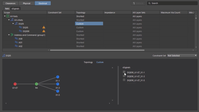
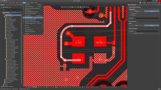
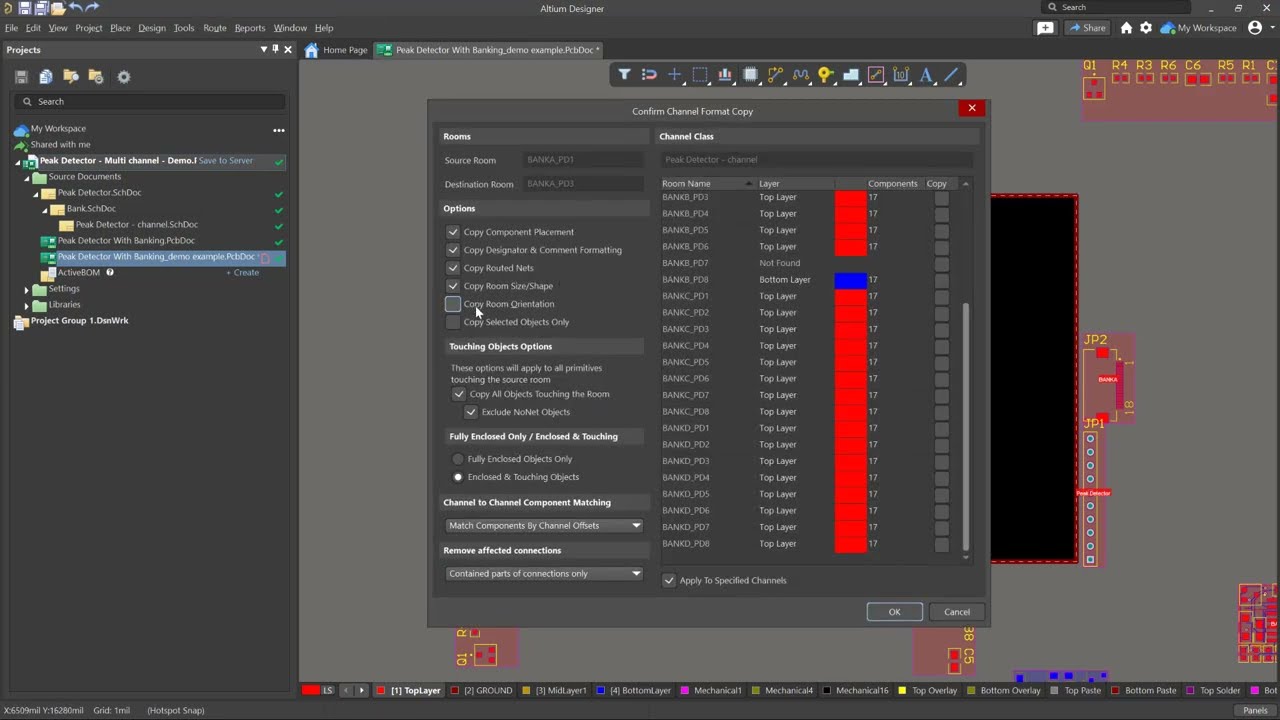
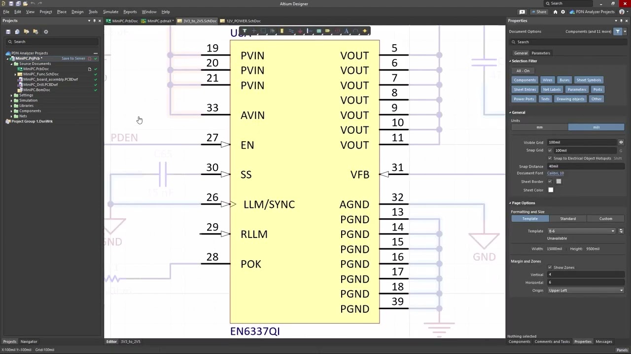
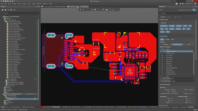
Constraint Manager Improvements
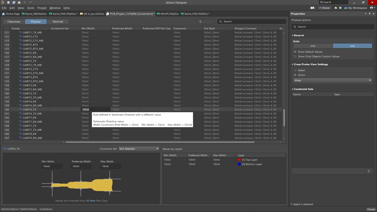
Automatically Propagate Width Values in the Constraint Manager
You can now enter a width value into a single cell at the top grid area, and it will automatically propagate to all corresponding width or gap fields. Furthermore, when working from a schematic, there is an indication of the sync status between constraints defined in the Constraint Manager and those specified through design directives in the source schematics.
RECOMMENDED CONTENT
To see an overview about the Constraint Manager, visit the feature page.
To see the Constraint Manager in action, check out our recent webinar Empowering Faster Electronics Development with Altium Designer 24.
Check out our recent OnTrack Podcast video on the Constraint Manager, Deep Diving Into Altium Designer's New Constraint Manager.
Visit the documentation page to learn about the Constraint Manager.
Discover the latest features and capabilities of Altium Designer 24 with free training.
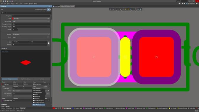
PCB Layout Enhancements
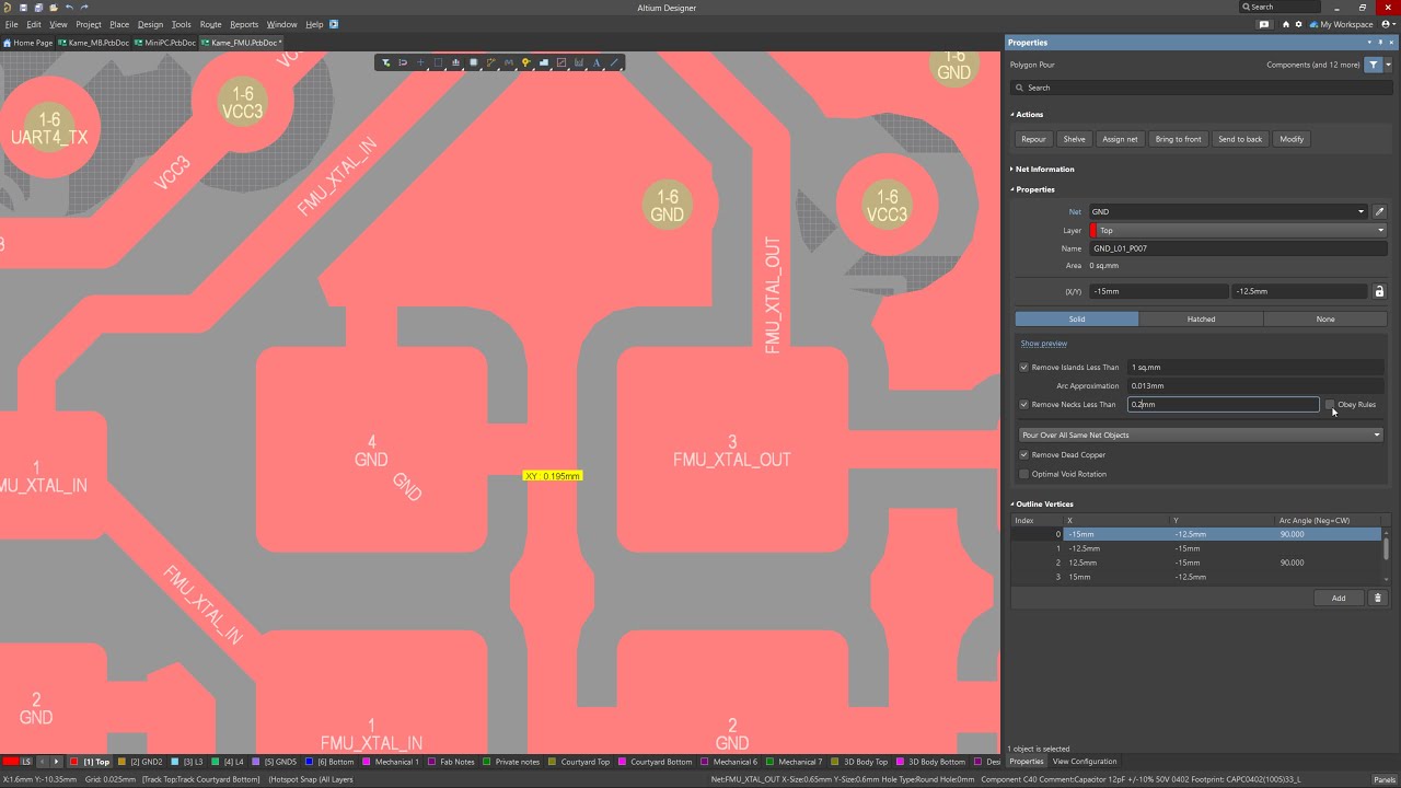
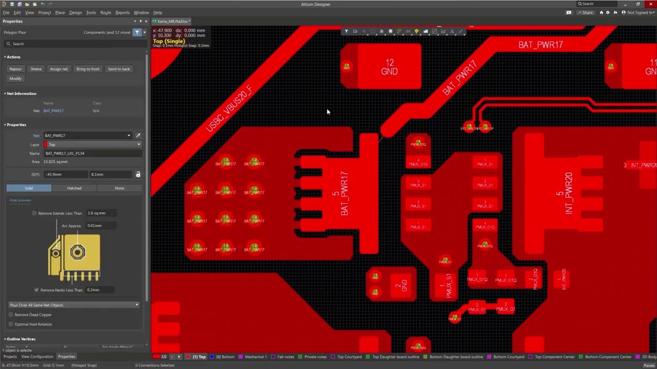
Remove Polygon Necks Less Than a Specified Width
With the new "obey rules" option in the properties panel, you now have the capability to remove necks less than a specified width for placed polygon pours. Furthermore, Altium Designer now observes user-defined geometries for the component selection bounding box when moving a component in Push Obstacles mode.
RECOMMENDED CONTENT
Visit the documentation page to learn about PCB Layout.
Discover the latest features and capabilities of Altium Designer 24 with free training.
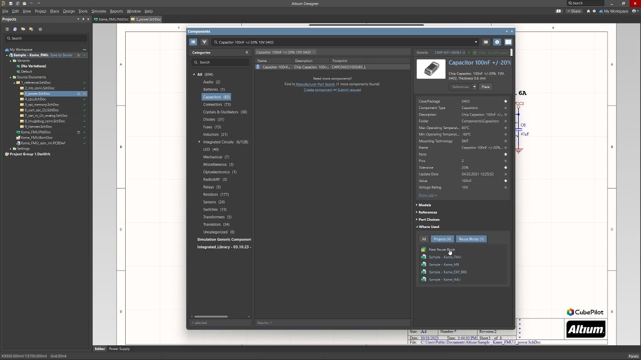
Data Management Improvements
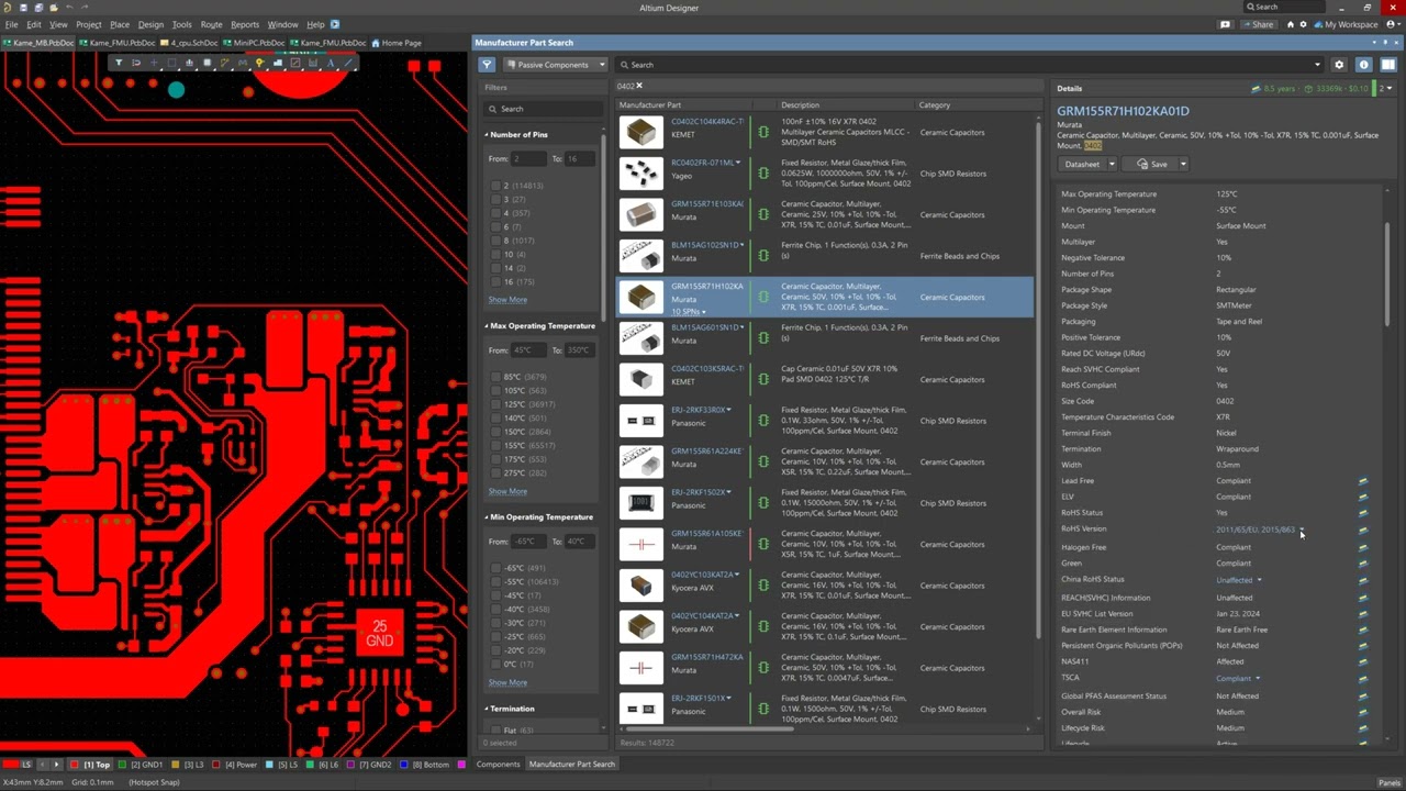
See the Exact YTEOL Value for Your Components
The real value for years to end of life parameter is accurately displayed across all instances where SiliconExpert data is presented, ensuring clarity and precision in your design process. Additionally, we’ve added support for referencing SiliconExpert compliance datasheets, enhancing accessibility and usability. We’ve also included support for the newest Microsoft Access Database file format when synchronizing Database to Workspace components.
RECOMMENDED CONTENT
To see an overview about the Manufacturer Part Search, visit the feature page.
Visit the documentation page to learn about the searching and placing components.
Discover the latest features and capabilities of Altium Designer 24 with free training.
Altium Designer 24
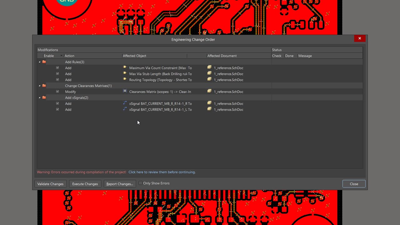
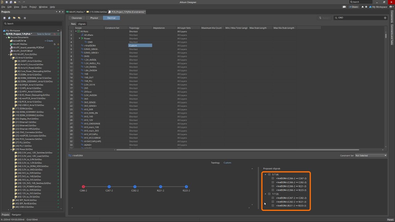
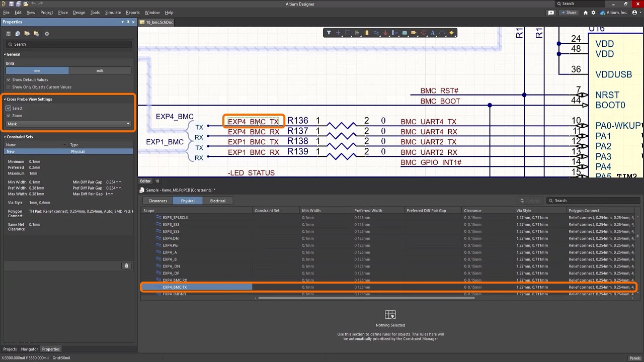
约束管理器改进
使用约束管理器确保准确的电气间距
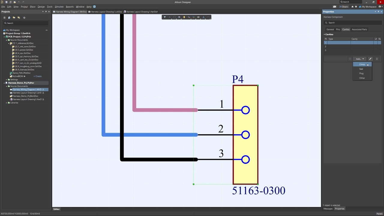
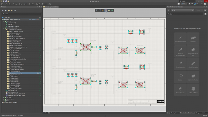
线束设计改进
为每个线束元件引脚指定详细信息
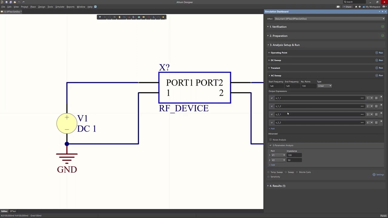
仿真改进
使用S参数进行网络表征
约束管理器改进
在PCB和原理图间传输设计约束
线束设计改进
在线束设计中将导线设置为多色
约束管理器增强
借助约束管理器体验更高控制水平
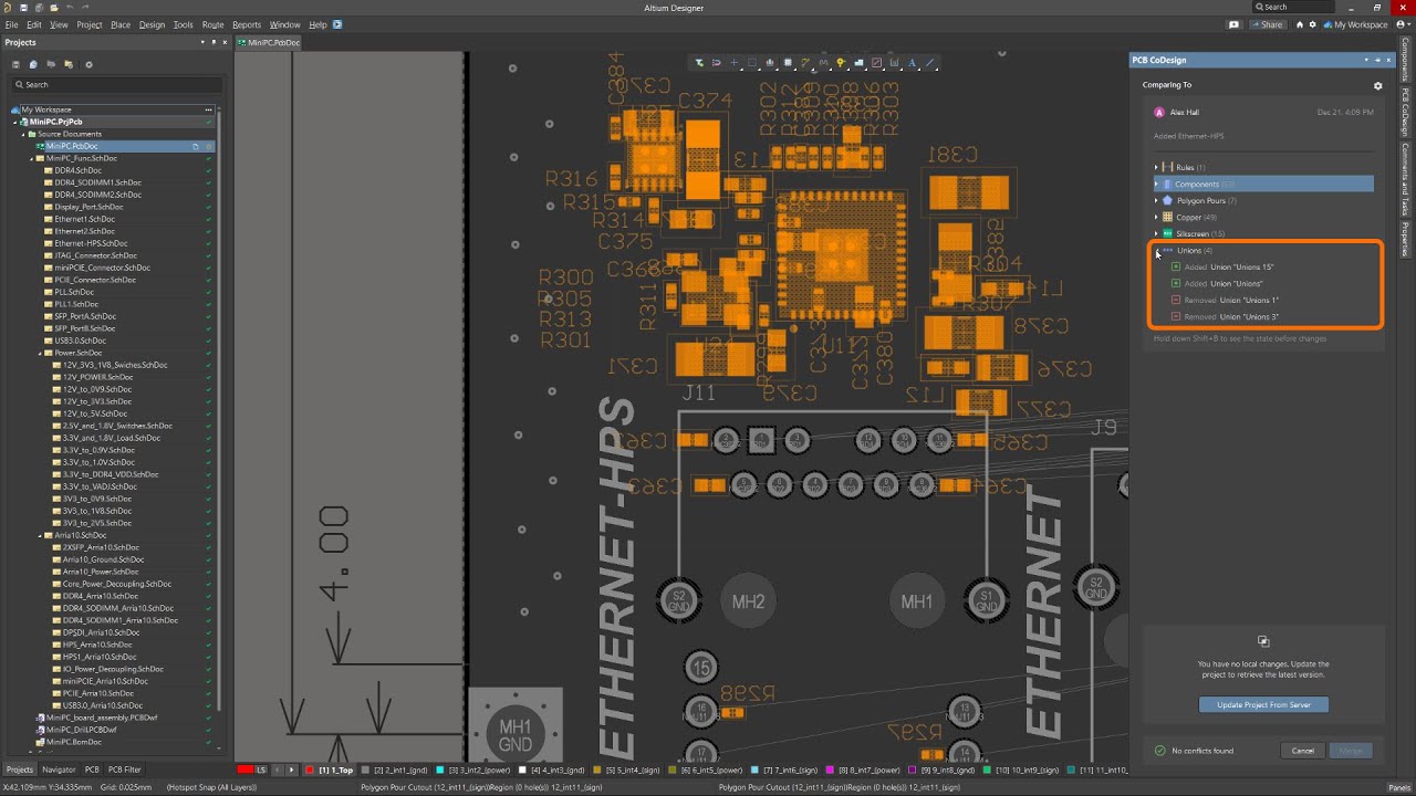
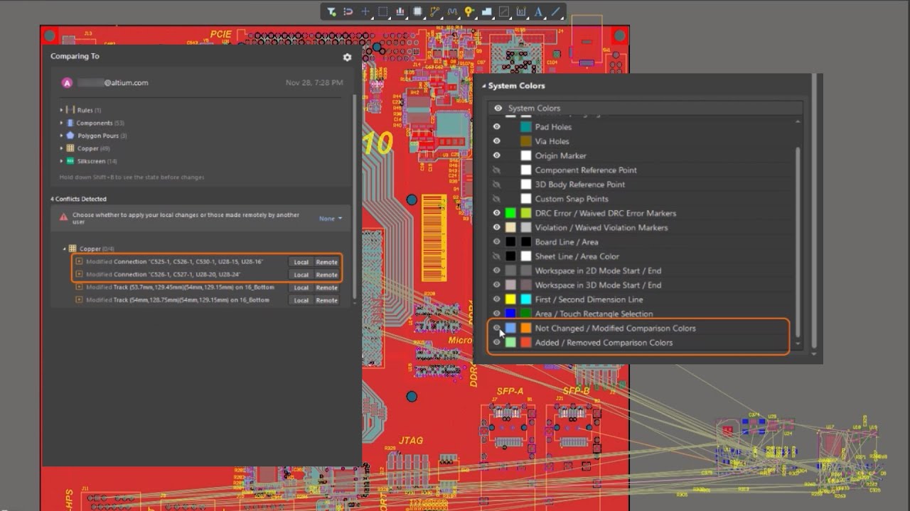
PCB 协同设计改进
借助 PCB 协同设计突出显示特定的已修改类别
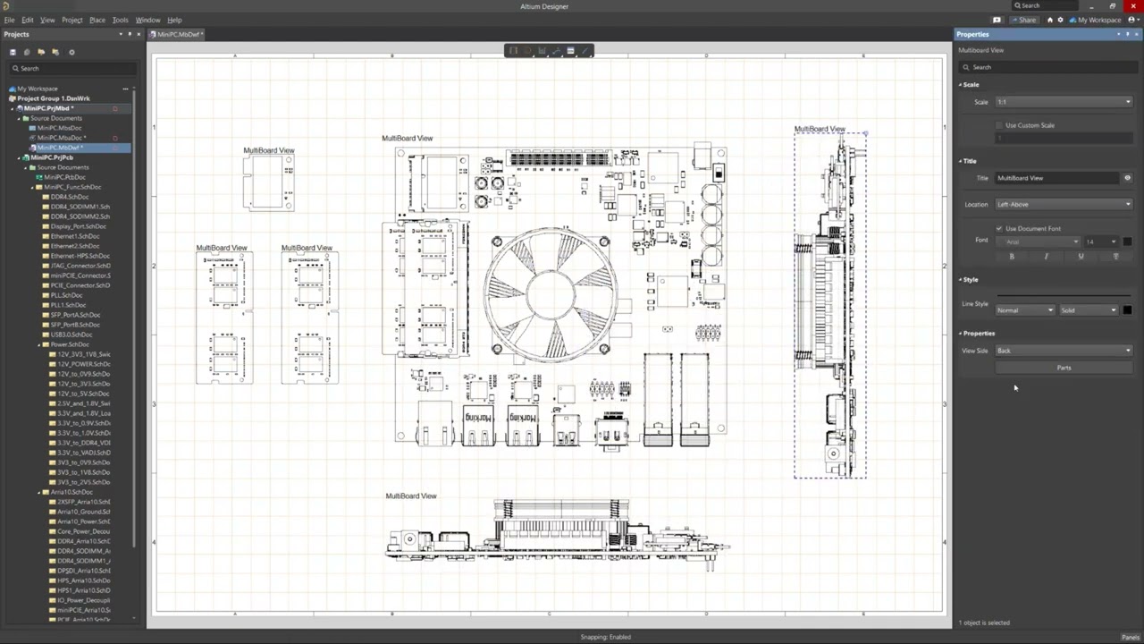
多板改进
为您的多板项目创建清晰的可视化表现形式
使用约束管理器简化复杂的设计规则
使用 PCB 协同设计加速设计进程
使用 3D 机电集成器件工具提升项目水平
Altium Designer 23
使用约束管理器应对任何设计复杂性
PCB改进
以任意角度重塑单端走线
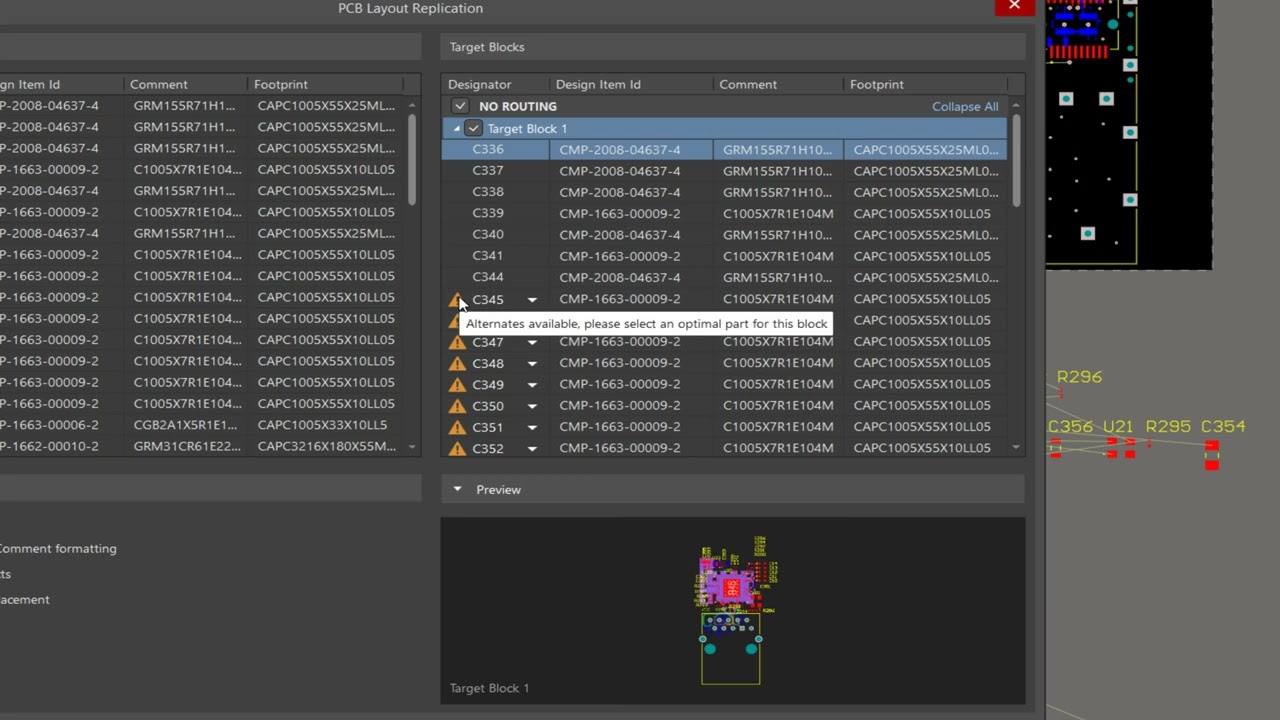
元件管理改进
使用“Where Used”面板跟踪复用块中的元件
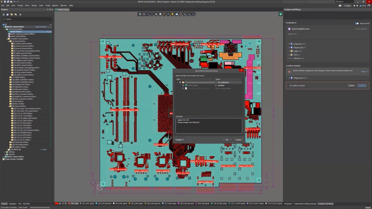
协同改进
通过PCB CoDesign功能实现高效协同设计
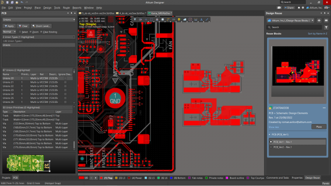
对于Pro版和Enterprise版订阅,Altium Designer中的PCB CoDesign功能将确保多名团队成员能够同时处理一个项目,以通过简化开发流程,提高测试和迭代效率,如期完成项目,从而彻底改变了协同设计方式。此项功能包括一种类似于Git的版本控制方法,以确保协同人员能够同时访问同一项目,将更改提交至主分支,并使用Commenting and Tasks功能在电路板上进行工作分配。将会以通知的形式提醒团队成员进行提交,通过Compare and Merge面板显示设计差异,并按颜色编码提供反馈。当发生冲突时,例如多名设计人员重复更改,您可以根据需要自行选择保留本地更改,或者接受最新提交的远程更改,从而确保顺利开展协同设计工作。
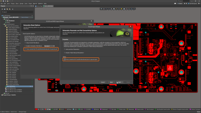
导入器增强功能
无缝导入OrCAD和Allegro设计文件
在将OrCAD和Allegro设计文件导入Altium Designer时,进行了关键性的改进和修复。这包括对自定义端口连接器的支持、准确的标题块参数处理、元件填充颜色保留以及精确的设计文件导入,从而确保您的设计过程无缝进行。
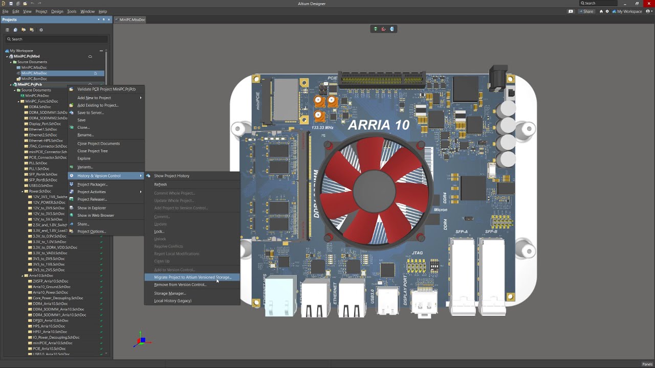
SVN 到 Git 迁移
将设计项目从 SVN 迁移到 Git
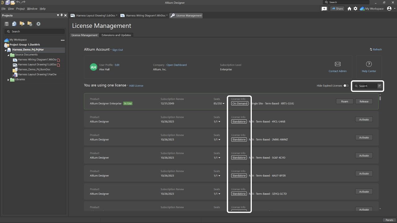
许可证管理改进
通过增强导航和标签功能,优化许可证管理
PCB 协同设计改进
添加了 Room 方向保持功能
PCB 协同设计改进
添加了可用于制造和装配说明的新特殊字符串
PCB设计改进
轻松管理设计中每个元件的零部件选择
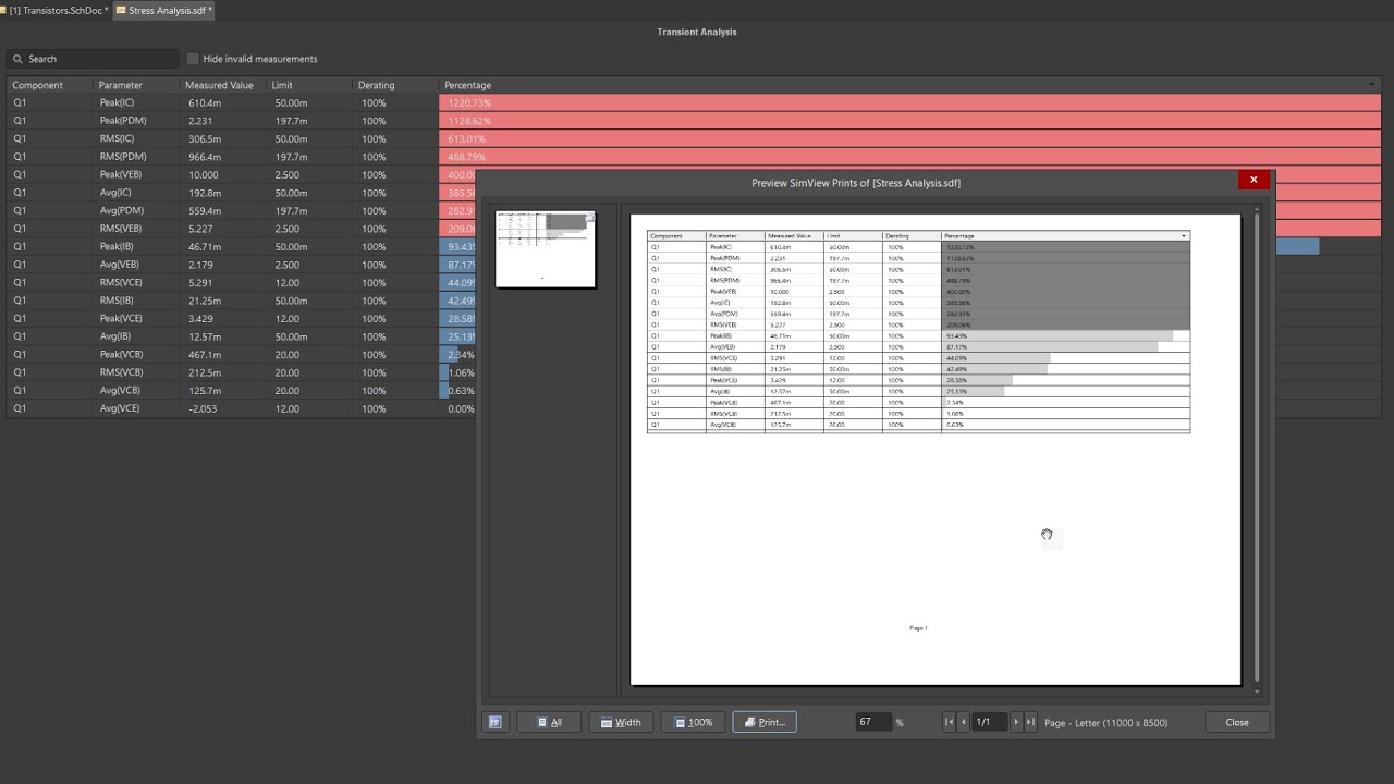
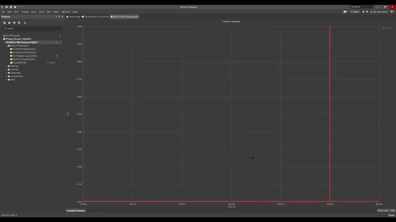
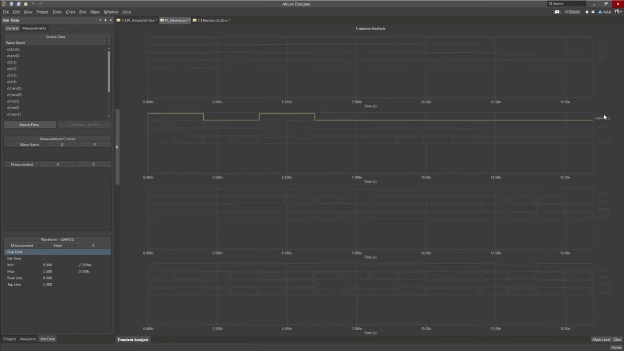
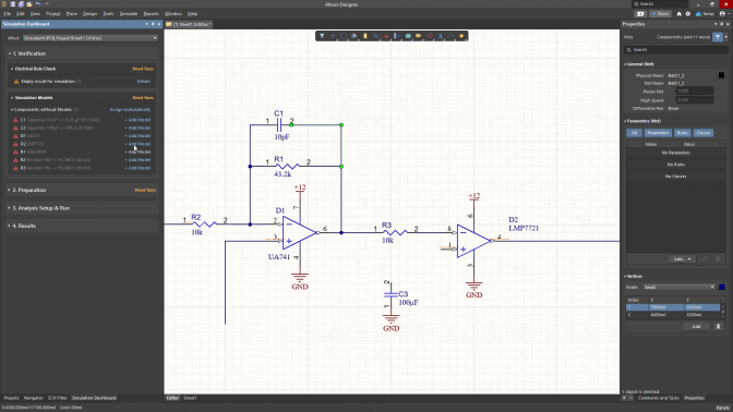
电路仿真改进
使用新仿真数据查看器精确测量结果
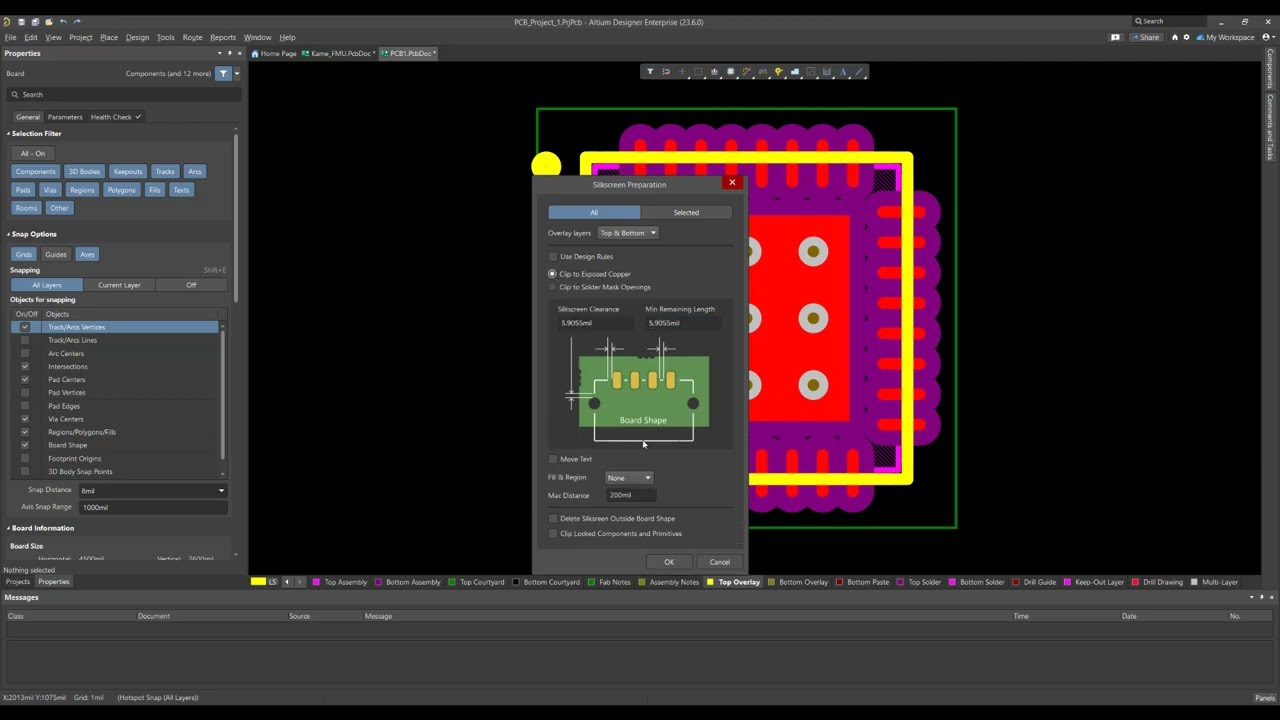
PCB 协同设计改进
精确定位丝印,为封装创建和 PCB 制造做准备
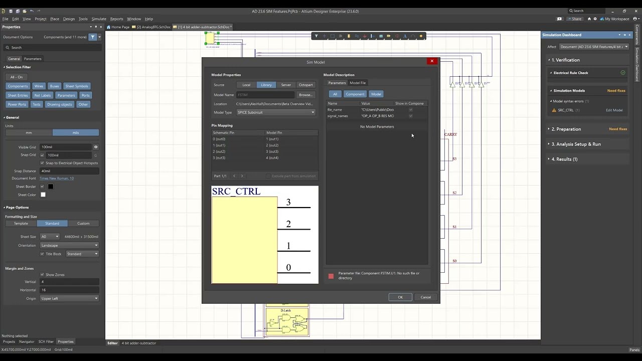
电路仿真改进
在仿真过程中使用 FSTIM 激励模型
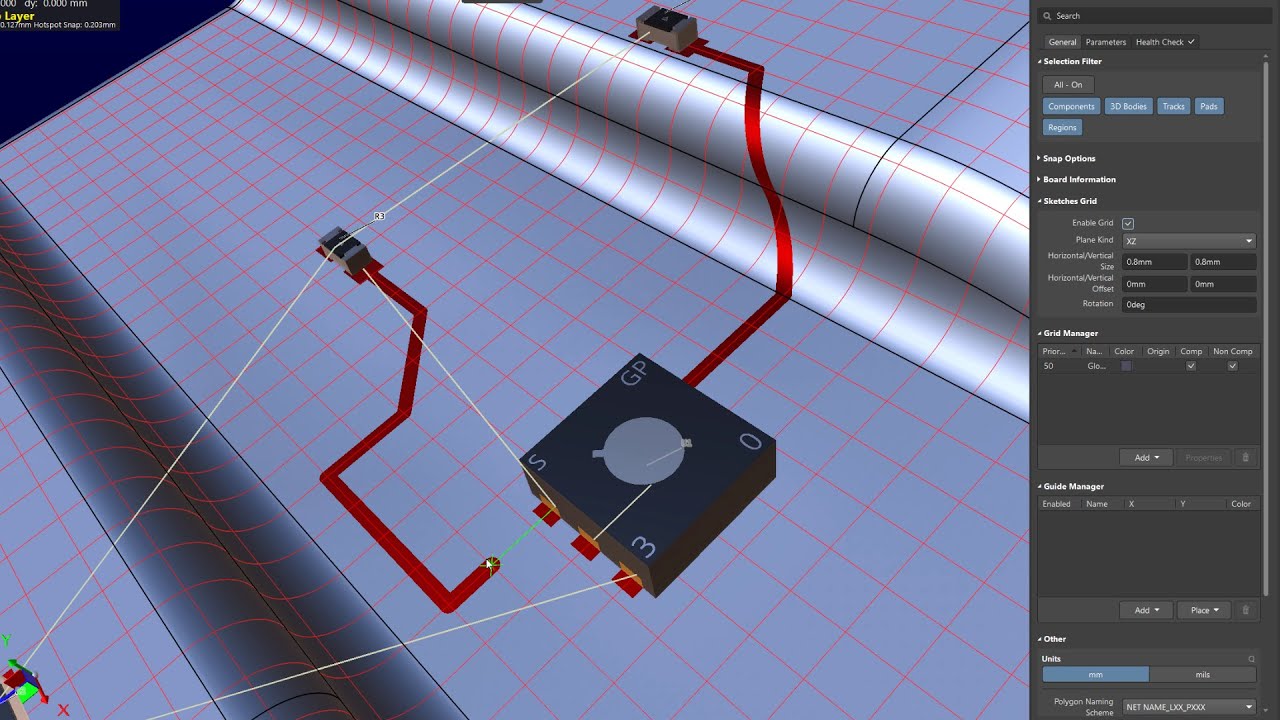
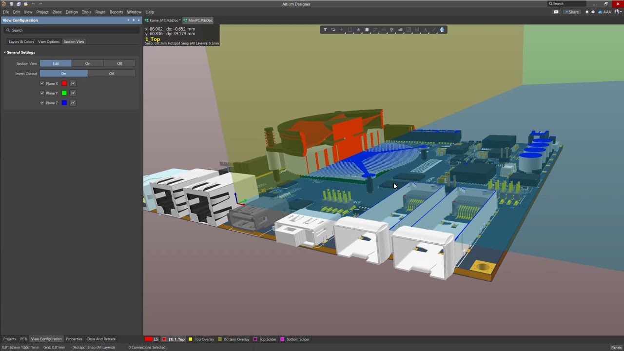
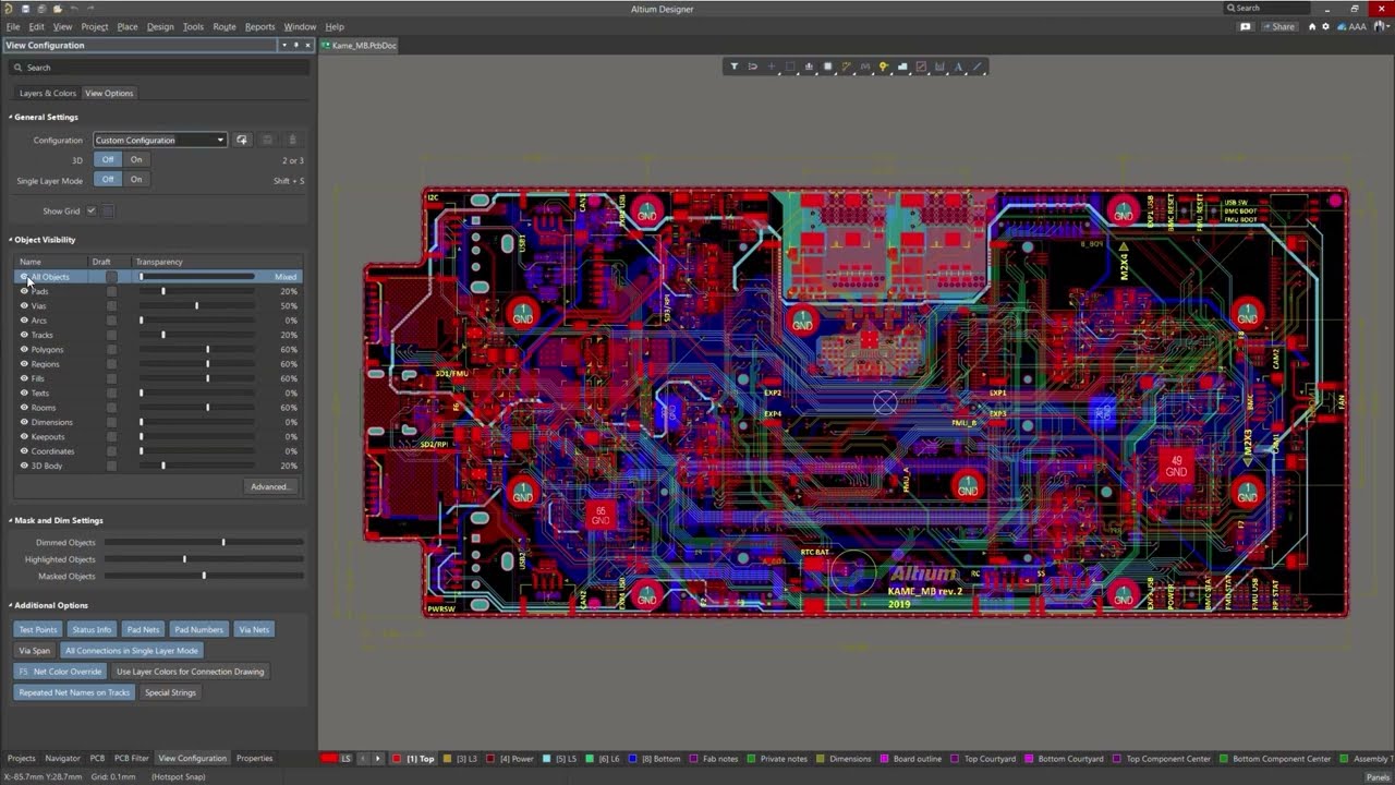
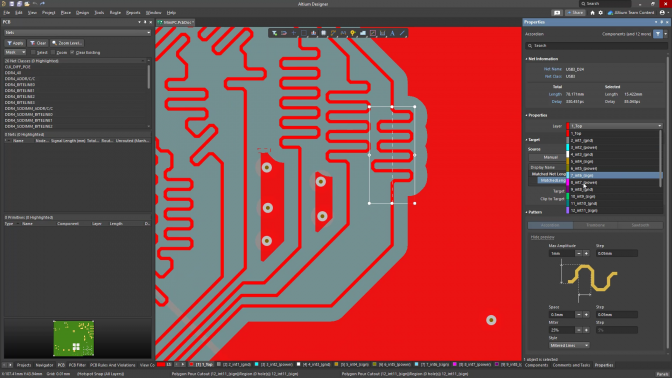
使用 PCB 剖面图功能查看隐藏元件
PCB 的剖面图功能为您的设计提供了前所未有的精确洞察,揭示了 PCB 布局和结构中通常不可见的细节。当处理密集和复杂的 PCB 时,剖面视图可以显示 PCB 中的细节。通过控制平面的放置和颜色,您可以轻松查看所有元件,甚至是隐藏在较大元件或机械零部件下的较小 SMD 元器件。
定制热风焊盘
使用实时仿真探测来测试您的电路
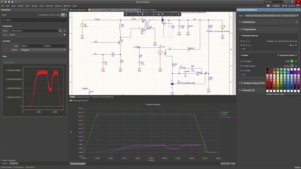
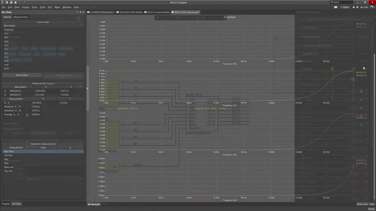
电路仿真支持受控源和可变无源器件在交流分析中的输出值
我们添加了对电压和电流受控源、函数信号源和可变无源器件的支持,以在进行交流分析时对电压、功率和电流输出变量进行分析。此功能非常适合音频项目、通信设计等设计类型。此外,我们还添加了对多位ADC和ROM PSPICE数字模型基元及其时序模型的支持。
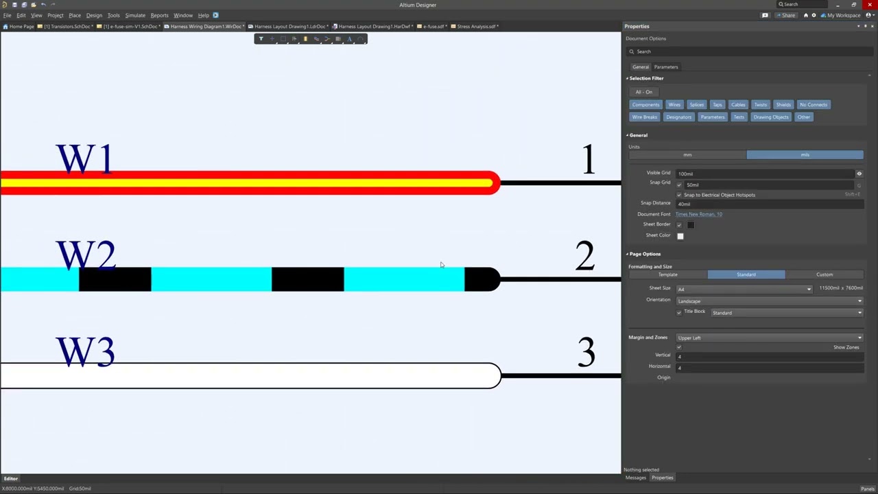
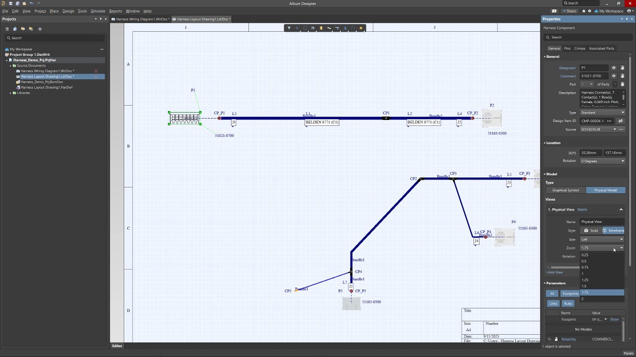
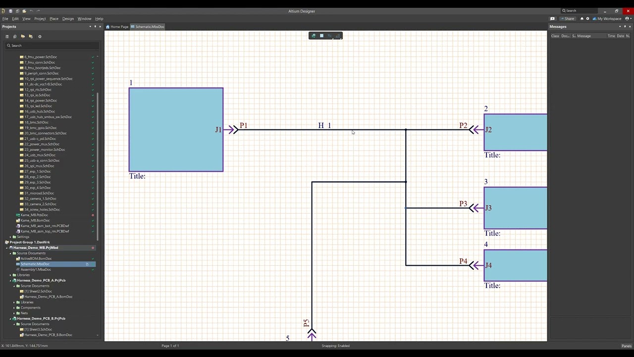
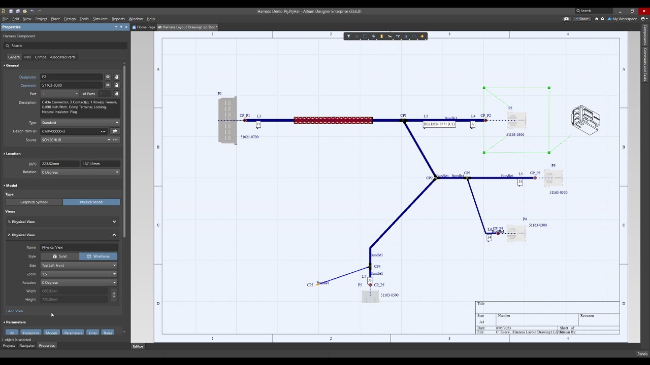
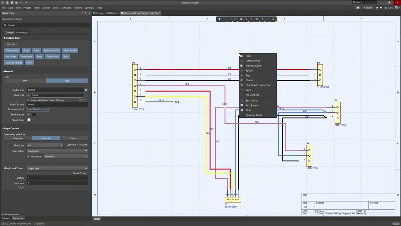
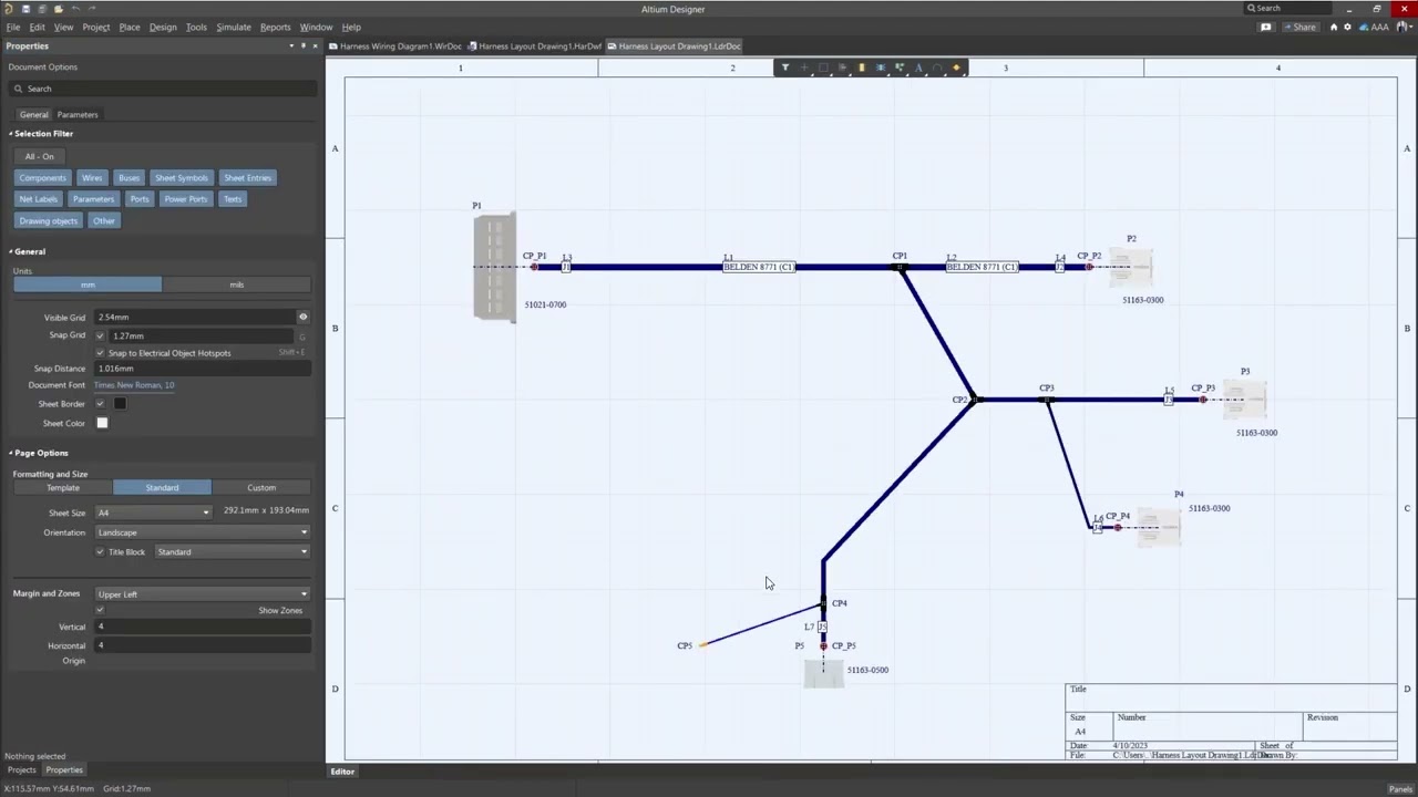
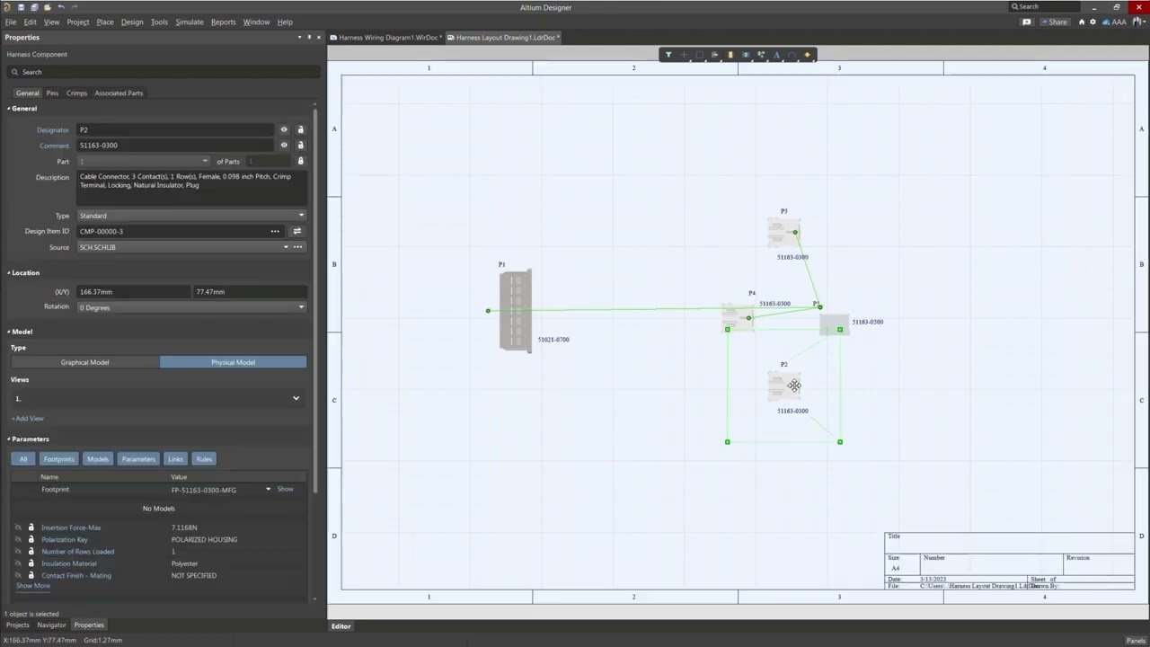
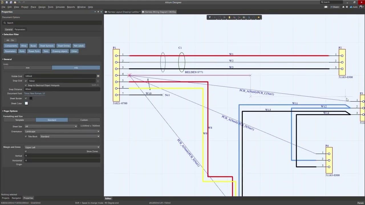
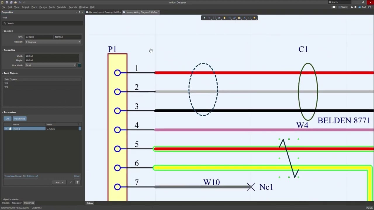
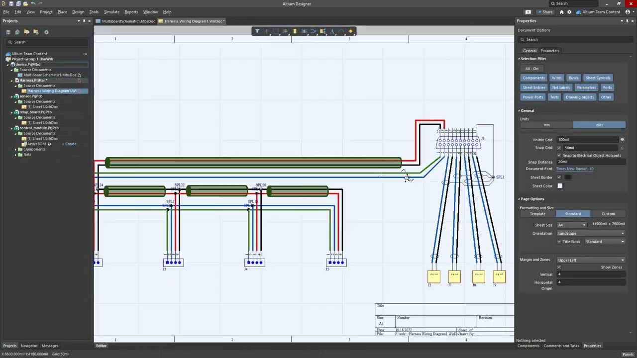
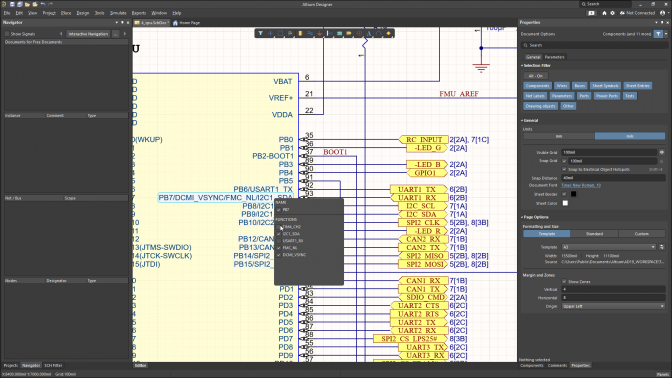
线束接线图对象的实时跟踪和固定纵横比
进行实时跟踪时,操作将主动跟随光标,直接向您展示通往最终导线目的地的路径。从而确保您能够在接线图中更加有效地追踪数据。接线图对象此时将与文档捕捉栅格同步,以将接线图统一性提升至一个新的水平。
线束设计新功能:3D 线框视图和向连接点添加模型
PCB 改进
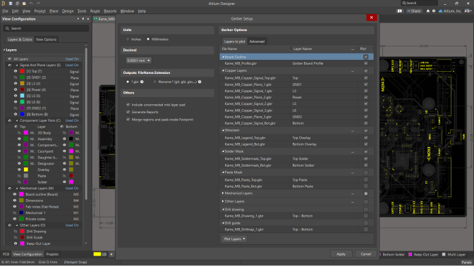
Gerber Setup 层类支持
电路仿真改进
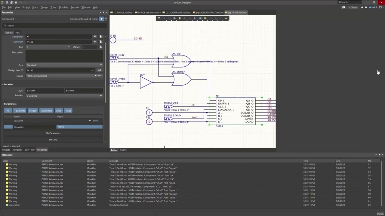
添加了对 PSpice 数字模型的支持
此版本的 Altium Designer 支持更多 PSpice 数字模型基元。我们添加了对 PINDLY 和 CONSTRAINT PSpice 数字行为模型基元的支持,以及对 DIGERRDEFAULT 选项的支持。
线束设计改进
线束设计改进
数据管理改进
协作和报告更新
线束设计改进
其他线束设计能力
PCB改进
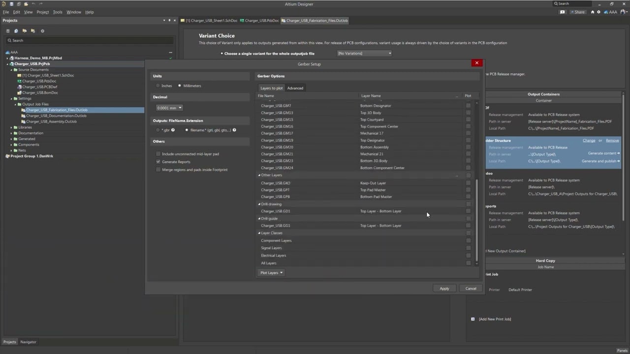
用于 Gerber 和视图配置的全新 PCB 功能
这个新的 PCB 功能允许您从视图配置面板加载存储的视图配置文件。此外,在使用新的统一 Gerber/Gerber X2 对话框时,现在还可以更改 Gerber Board Profile 图层的名称。
SIMULATION IMPROVEMENTS
New Extension For Power Integrity Analysis
Quickly assess the integrity of your power distribution network without the need for any specialized training with Power Analyzer by Keysight.
PRODUCT DESIGN IMPROVEMENTS
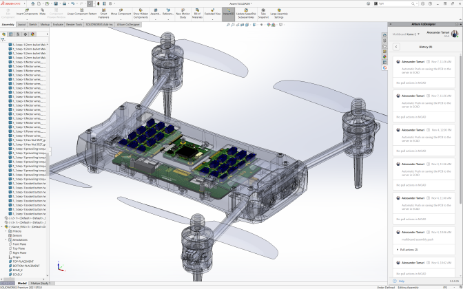
Multi-board support In MCAD CoDesigner
You are now able to transfer and sync your muli-board designs with your mechanical team using the MCAD CoDesigner.
产品设计改进
全新线束设计功能
Altium Designer 22
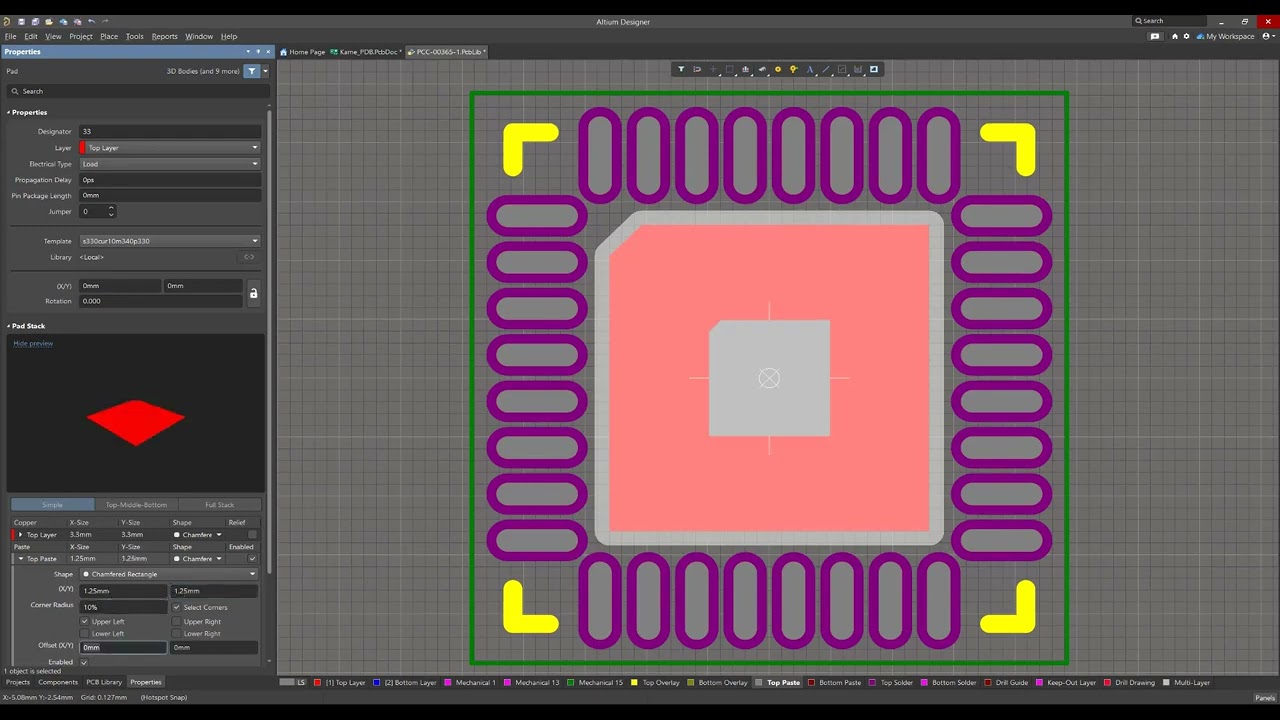
PCB Improvements
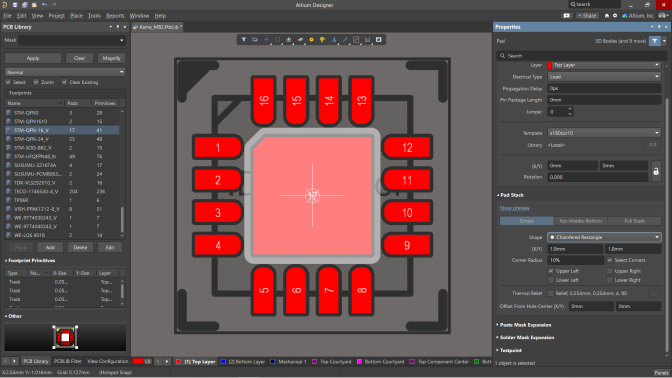
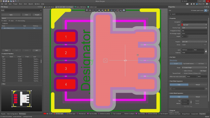
Custom Pad Shapes with Rounded/Chamfered Corners
Shape your pads the way you need in a matter of clicks. Extending the versatility of pad shapes, you can now customize the rounding of selected corners of pads that use either the Rounded Rectangle shape or the new Chamfered Rectangle shape.
PCB Improvements
Enhanced Gerber Setup Interface
Efficiency, simplicity and convenience are all delivered with the new UI for Gerber setup. Everything you need to prepare for Gerber generation is now at your fingertips in an intuitive setting.
SPICE SIMULATION IMPROVEMENTS
Additional Digital Models & Variant Support
Expanding the functionality available to you in the simulation arena, this release adds further support for PSPICE digital gates, timing and I/O models. Support for variants is also now available.
Data Management Improvements
Improved Manufacturer Part Search UI
The Manufacturer Part Search panel has long been a source of components for many users. Improvements have been made in this release that make it easier to use components in their libraries. This allows you to spend more time on development than on the process!
PCB Improvements
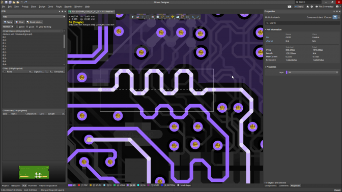
Additional Net Information for Tuning Objects
Detailed net information about tuning objects has been added in this release. Information about the maximum current and active resistance of accordion, sawtooth, and trombone objects is now available. More detail means it is less likely mistake will be made!
Schematic Capture Improvements
Quickly View Multi-function Pin Names
A large number of microcircuits have multi-functional pins. Working with them in Altium Designer has become even easier. This release introduces the ability to display the alternative pin names with just one click.
Schematic Capture Improvements
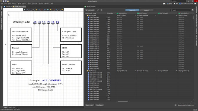
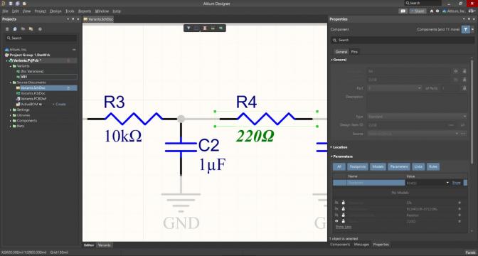
Improved Variant Management
Variant management is taken to the next level with this release. Time spent creating and editing variants is greatly reduced. Now you can design with large numbers of variants with streamlined ease and efficiency.
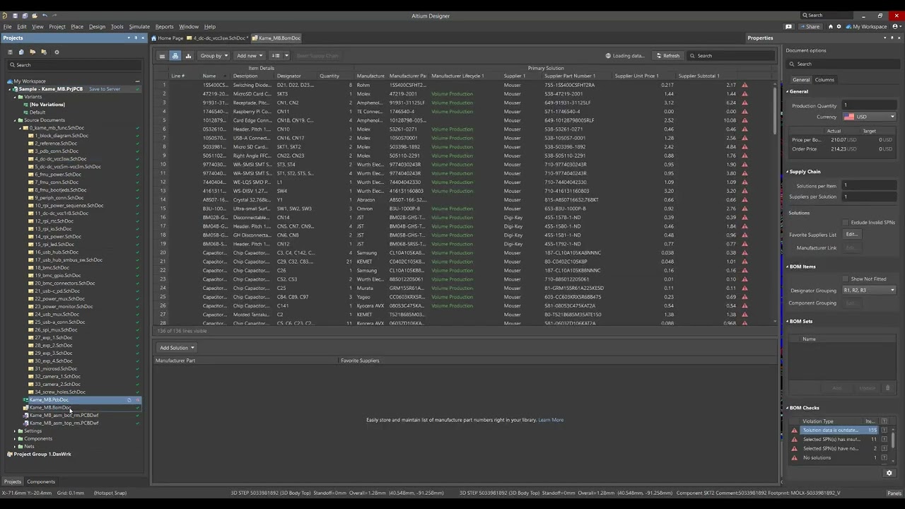
Data management improvements
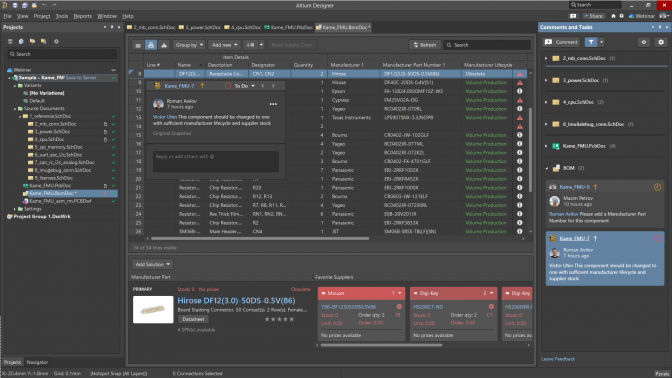
BOM Commenting
Support for commenting has arrived in the BOM arena with this release. All stakeholders can actively discuss the BOM with ease and convenience, as enjoyed already with schematic and PCB documents.
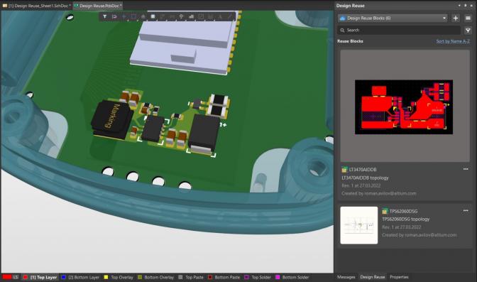
Data Management Improvements
Alternative PCB Layouts in a Reuse Block
Reuse Blocks are enhanced further in this release. You can now define multiple, alternate PCB layouts for use with a single block. When placing a block, quickly switch layouts to suit your physical and performance needs.
Data Management Improvements
Design Reuse Functionality
Take the enhanced functionality of Reuse Blocks for a spin in this release, with the ability to place a block (or schematic snippet) as a sheet symbol. Your proven circuitry is placed on an auto-generated child sheet.
Schematic Capture Improvements
Mark Multiple Components as Fitted/Not Fitted
With this release it becomes even easier to work with multi-variant design projects. Now you can select multiple components for the active variant and mark them as Fitted/Not Fitted in a single action.
PCB Improvements
Custom Pad Shapes
Modern components often contain pads that are complex in shape. This release of Altium Designer gives you the ability to create custom pad shapes quickly and easily, with management similar to that of standard pads.
PCB Improvments
Ability to Change Tuning Object Layer Properties
Design of high-speed PCBs becomes easier with this latest release. Now, when you need to quickly move tuning elements to a different layer, you can do so from the Properties panel with a single click.
SPICE Simulation Improvements
Auto-assign Simulation Models for Components without Models
This latest version of Altium Designer makes schematic simulation even easier. System intelligence automatically recognizes SPICE models and assigns them to components from available sources.
Output Improvements
Control of Paste Mask Output for Variants
Output data needs to be as accurate as possible. For multi-variant designs you can now ensure that the paste mask is only displayed where it is really needed.
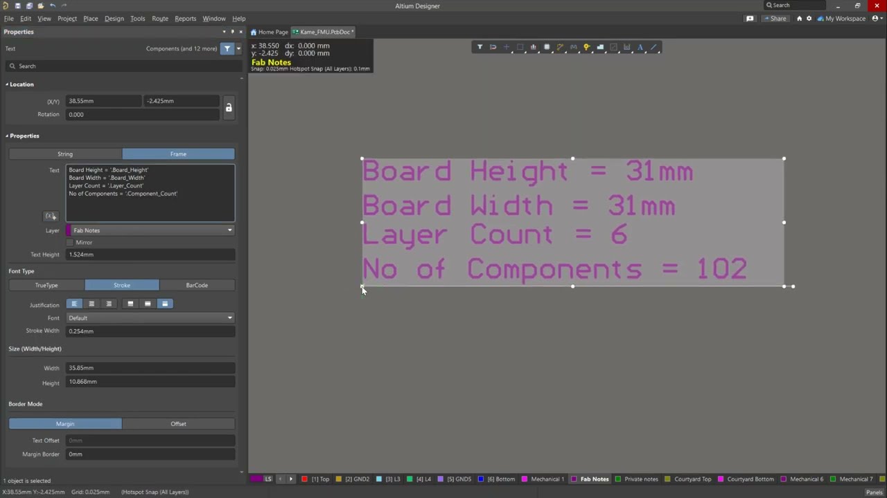
PCB Improvements
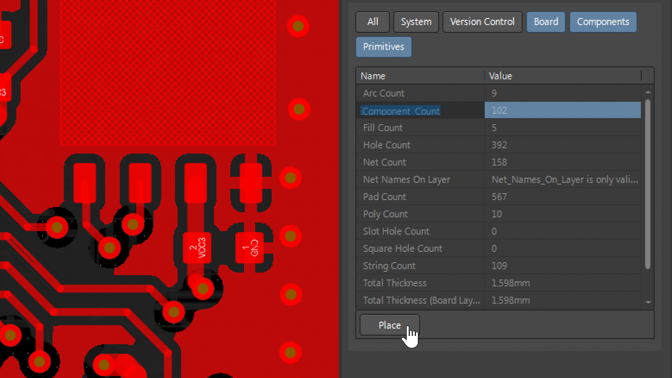
Quick Browsing of Parameters for a Board
Parametric information for your board is now conveniently available from the Properties panel. A single, convenient location with which to browse system, calculated and user-defined parameters, and place as needed in the form of special strings.
Schematic Capture Improvements
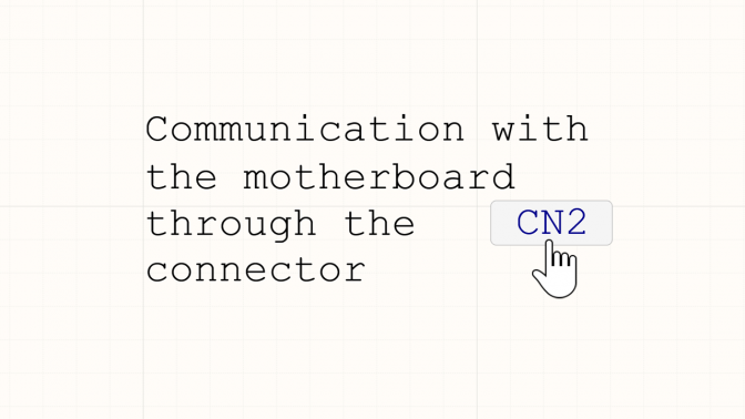
Active Links in Text
You can now specify active links to components and nets within a text frame object on a schematic. This handy navigation aid makes it much easier not only to read the document, but also to work with it.
Schematic Capture Improvements
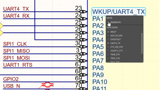
Multifunctional pins
You will often see that modern ICs consist of multi-functional pins. In this latest version of Altium Designer it has become far easier and much more convenient to work with such components.
Schematic Capture Improvements
Custom Diff Pair Suffixes
Even more possibilities for creating differential pairs. Now you can use any postfixes to designate positive and negative net of a differential pair.
PCB Improvements
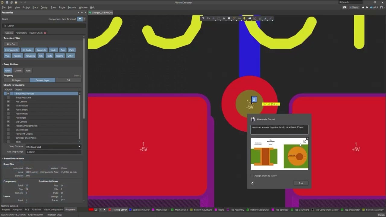
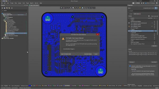
PCB Health Check Monitor
The condition of the PCB is under your control. A new intelligent feature that gives you confidence that your PCB is okay and complies with design rules.
Schematic Capture Improvements
Display of Alternate Component Parameters
Many schematic solutions are created as multivariant. With the new release, the schematic of multivariant project have become even more detailed and informative.
MultiBoard Improvements
Components from Altium 365
Working with multiboards has become easier and more convenient. Now you have more component sources at your disposal.
Data Мanagement Improvements
New Design Reuse Functionality
A reuse bloks help reduce development time and avoid errors. The new Design Reuse Panel and new functionality expands the possibilities for reuse blocks and snippets.
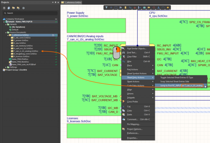
Further Enhancements to Sheet Cross-referencing
Schematic Capture Improvement
Adding cross-references to the project allows you to easily follow the connective flow of nets between the schematic sheets in a project.
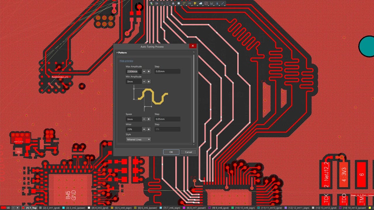
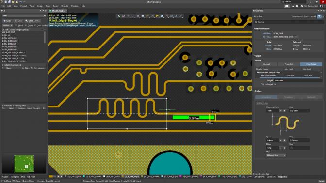
High-Speed Design Improvements
Relative Length Tuning
Designing high-speed PCB just got easier. The Length Tuning tools is now even more functionality. Complex tasks can now be solved even faster.
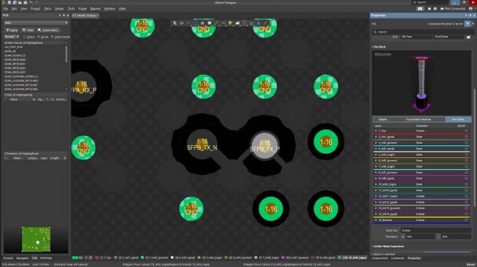
PCB Design Improvements
Enhanced UI for Via Stack Editing
The via editing mode is now even more convenient. Information about the via, editing its parameters and connections to polygons are now all in a new and simple, but familiar form.
Data Мanagement Improvements
Generic Components
The way from idea to real devices has become shorter. The new feature will reduce the time it takes to design a schematic.
 沪公网安备 31010502006411号