Altium Designer 新功能概览
探索 Altium Designer 最新版本中引入的新功能、改进和重要变更,
或查看我们正在为即将发布的版本所做的工作。
PCB Enhancements
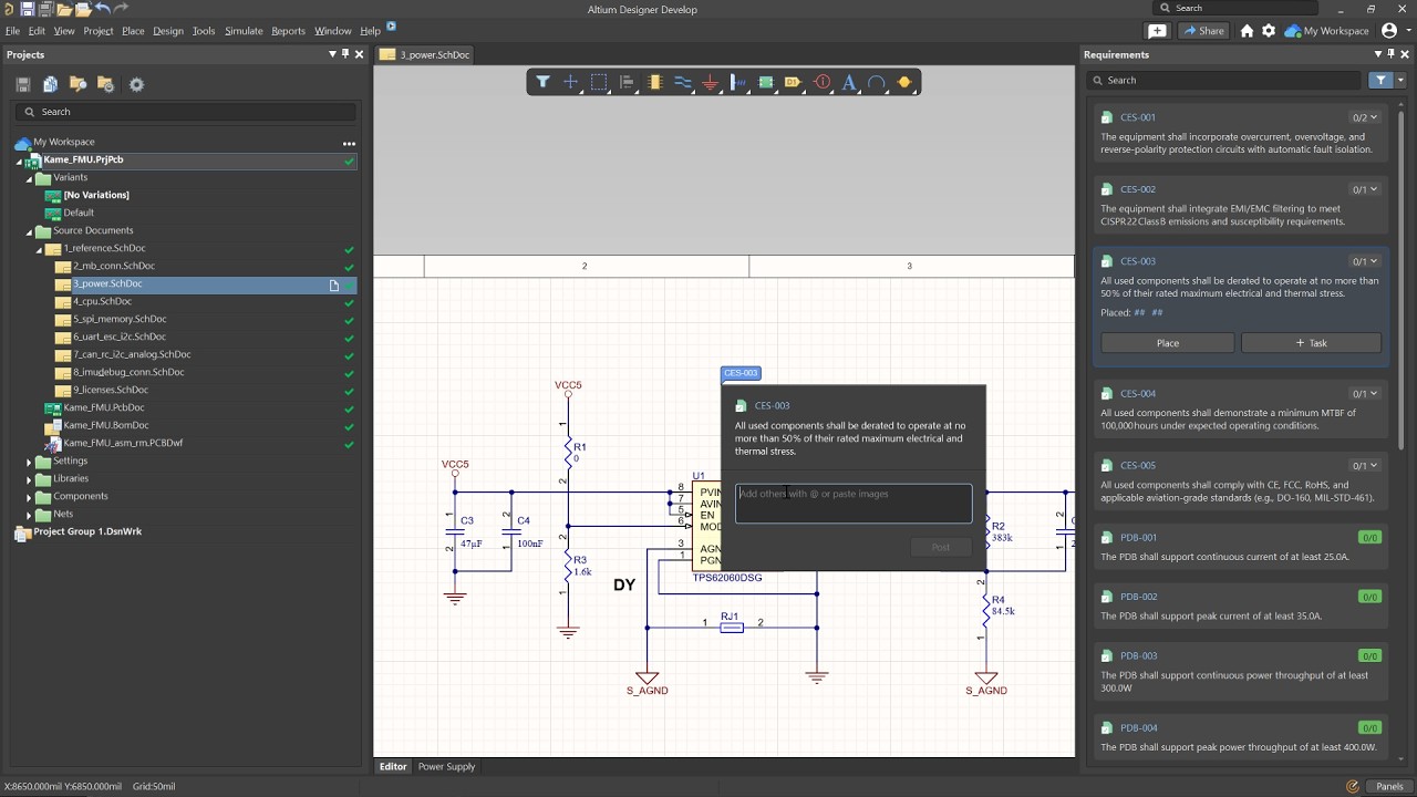
Connect Requirements Directly to Your PCB Design
The Requirements Portal integration in Altium Designer enhances PCB design by connecting system requirements directly to the design environment. You can place requirements on schematics or PCB documents, assign tasks, and track verification status in real time, ensuring data synchronization within Altium 365.
Recommended Content:
- Visit the Requirements Portal page.
- Learn more about the Octopart Discover, Altium Develop, and Altium Agile platform solutions.
PCB Enhancements
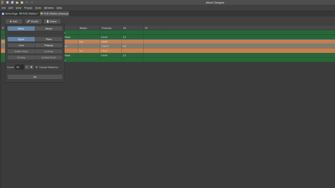
Handle High-Density PCB Layouts with Ease
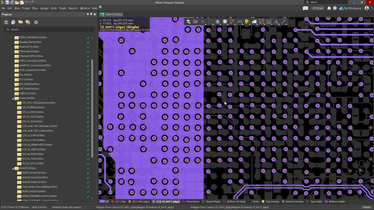
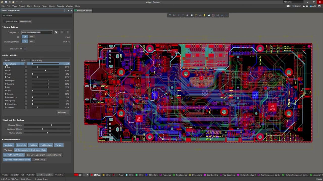
You can now create up to 128 signal layers in your PCB design, enabling the creation of more complex and high-density boards.
Recommended Content:
- To learn more about PCB Layout in Altium Designer, visit the resource page.
- Visit the PCB Layout documentation page.
- Learn more about the Octopart Discover, Altium Develop, and Altium Agile platform solutions.
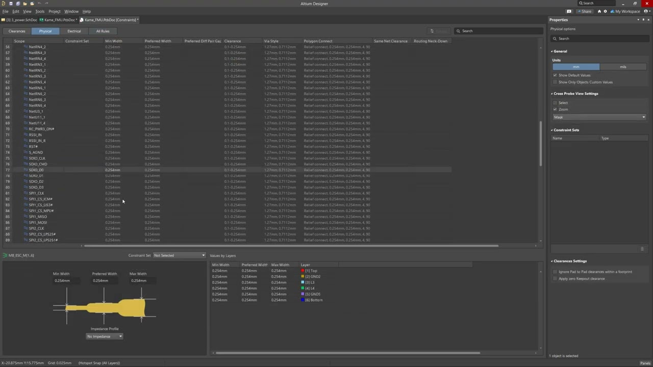
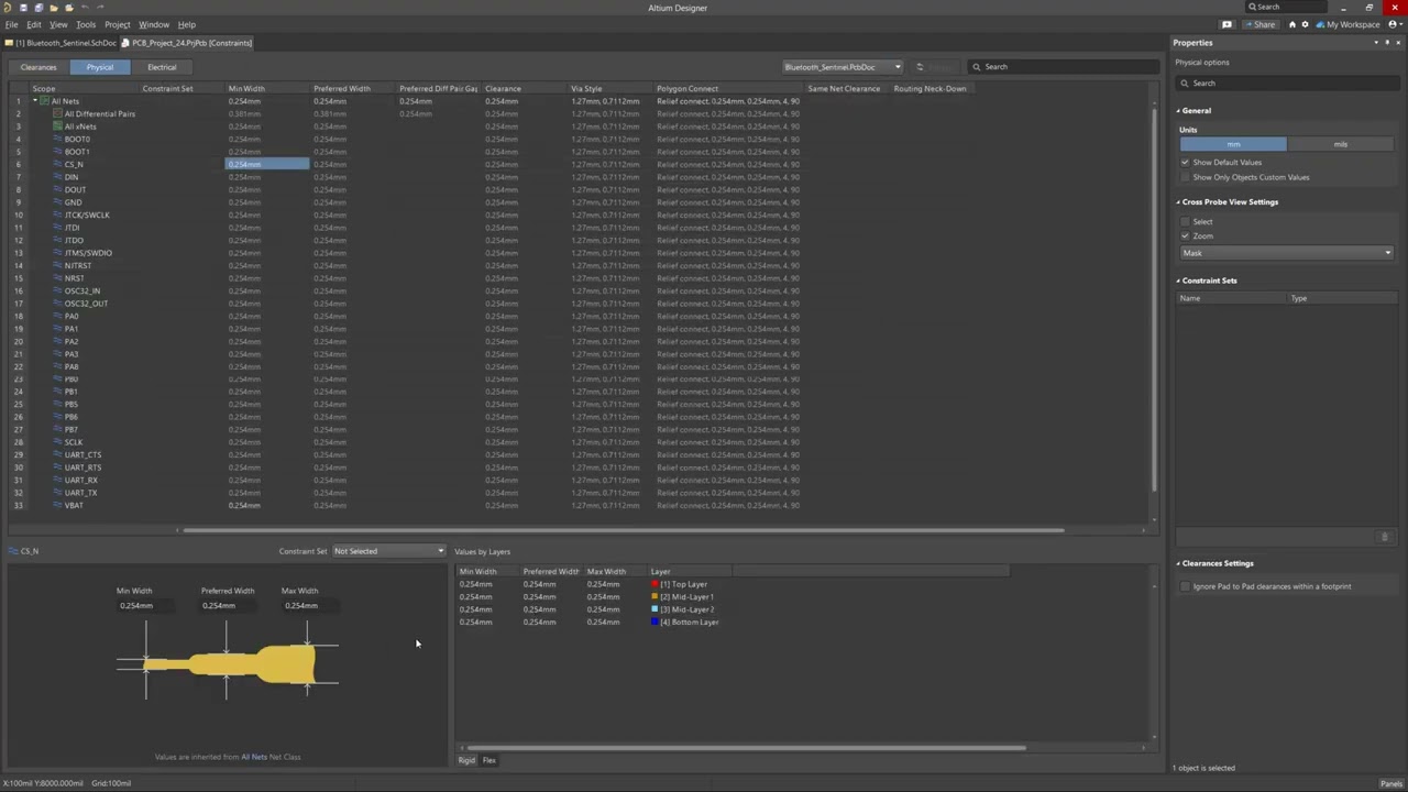
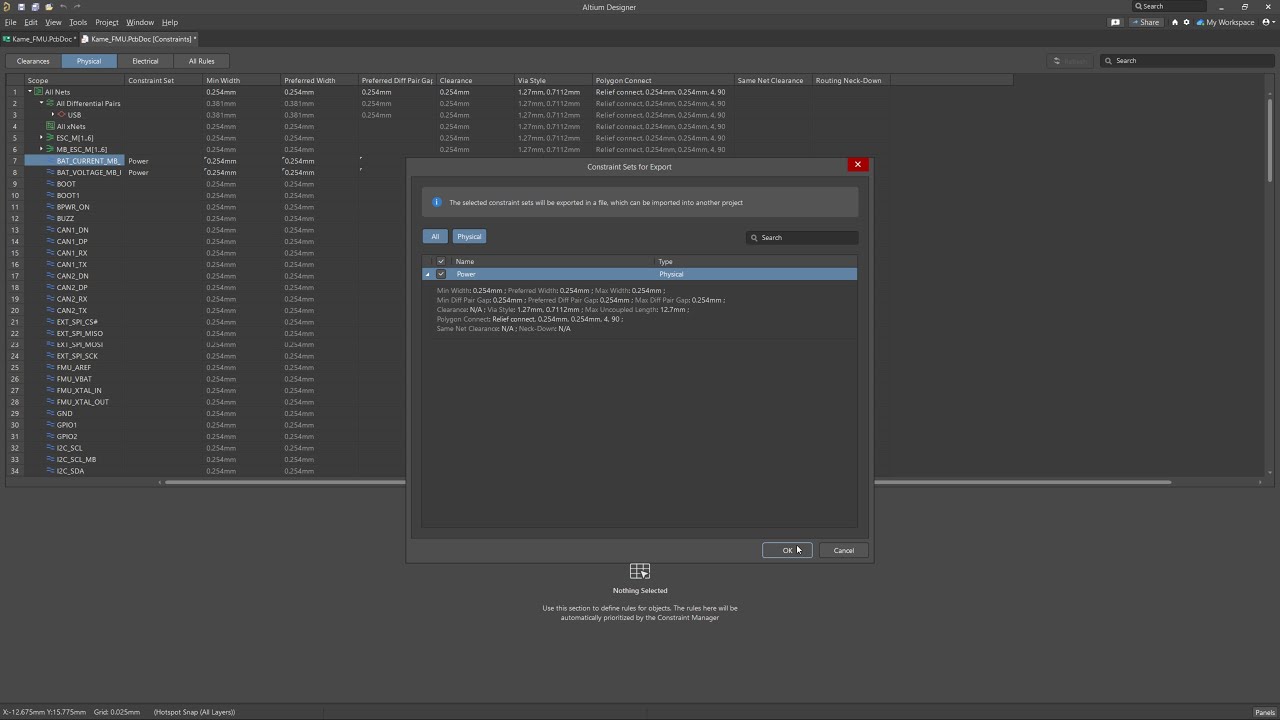
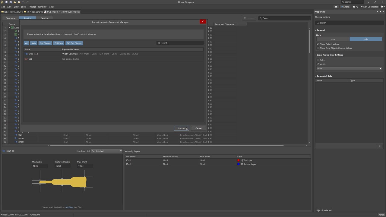
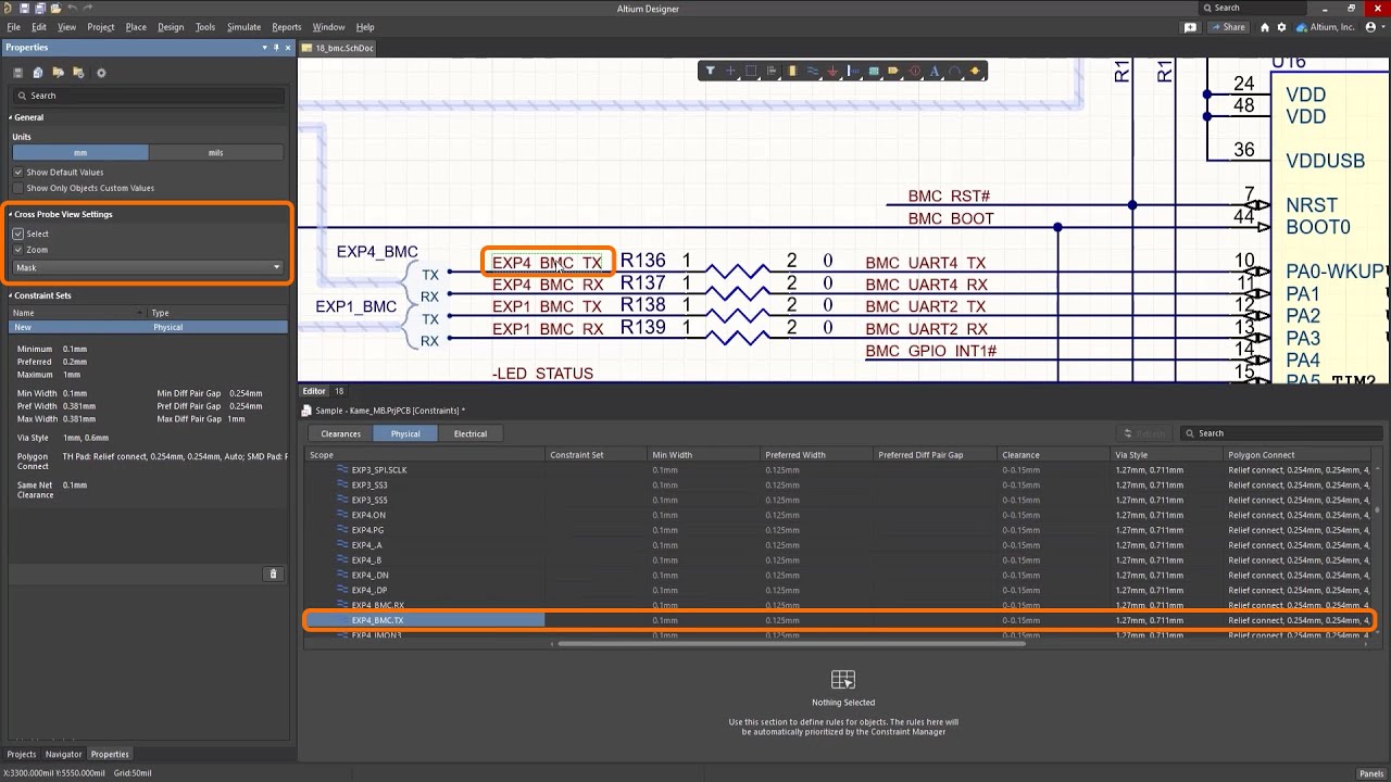
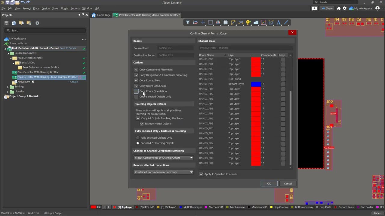
Constraint Manager Enhancements
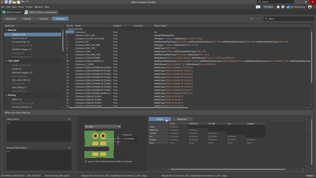
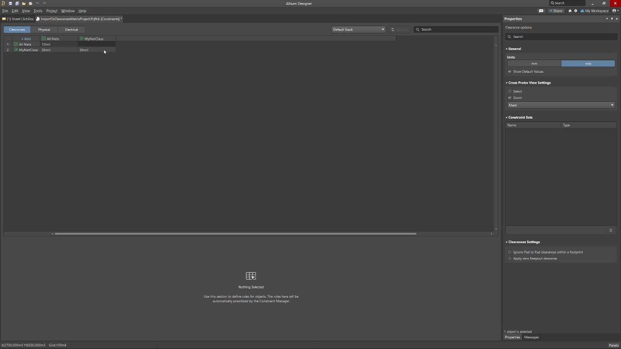
Create Clearance Rules Faster and with Less Effort
Clearance rule configuration in the Constraint Manager now includes Simple and Advanced views. The Simple view groups related object types to make rule setup easier, while the Advanced view provides a detailed clearance matrix for more precise control.
Recommended Content:
- To see an overview about the Constraint Manager, visit the feature page.
- Visit the Constraint Manager documentation page.
- Learn more about the Octopart Discover, Altium Develop, and Altium Agile platform solutions.
Altium Designer 26
Wire Bonding Enhancements
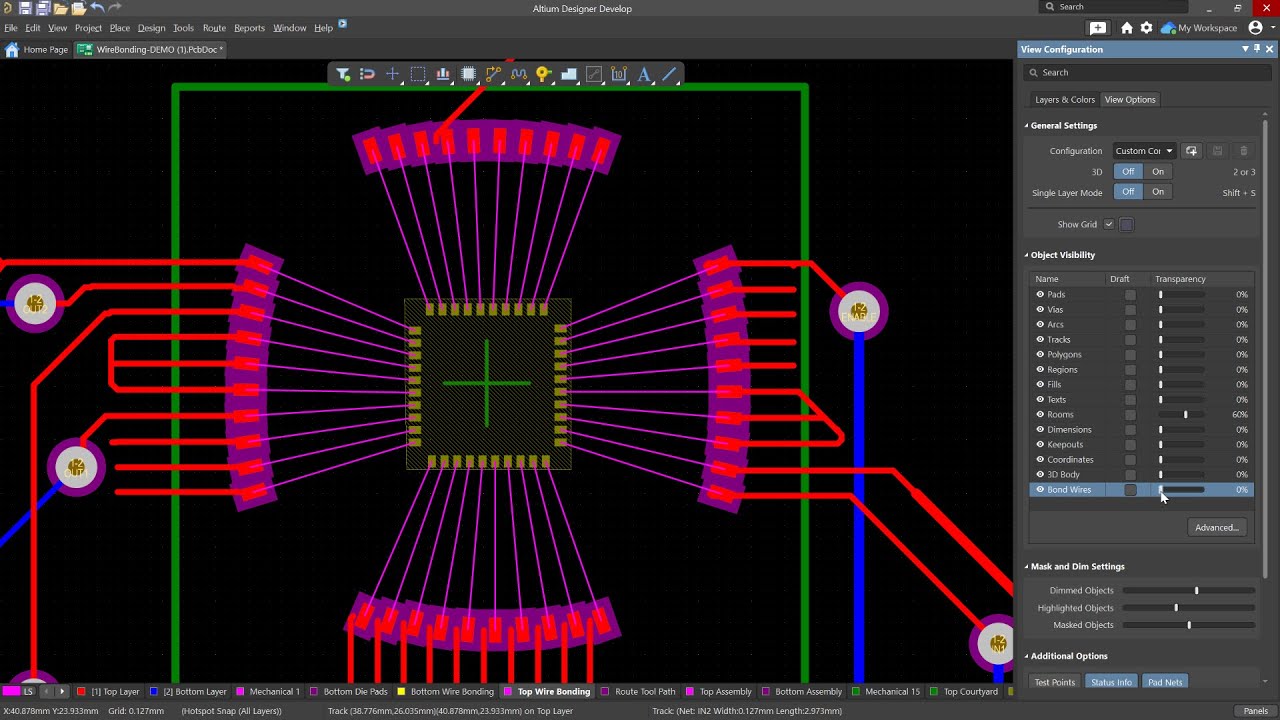
Gain Better Control Over Wire Bond Visibility
We've added new visibility controls for bond wires when working with boards or footprints that include wire bonding.
Recommended Content:
- To see an overview, visit the Wire Bonding feature page.
- Learn more about the Octopart Discover, Altium Develop, and Altium Agile platform solutions.
PCB Enhancements
Improve PCB Editor Performance with Via Instancing
The PCB editor now builds the geometry for each via instance rather than relying on a via template, using an approach called via instancing.
Recommended Content:
- To learn more about PCB Layout in Altium Designer, visit the resource page.
- Visit the PCB Layout documentation page.
- Learn more about the Octopart Discover, Altium Develop, and Altium Agile platform solutions.
PCB Enhancements
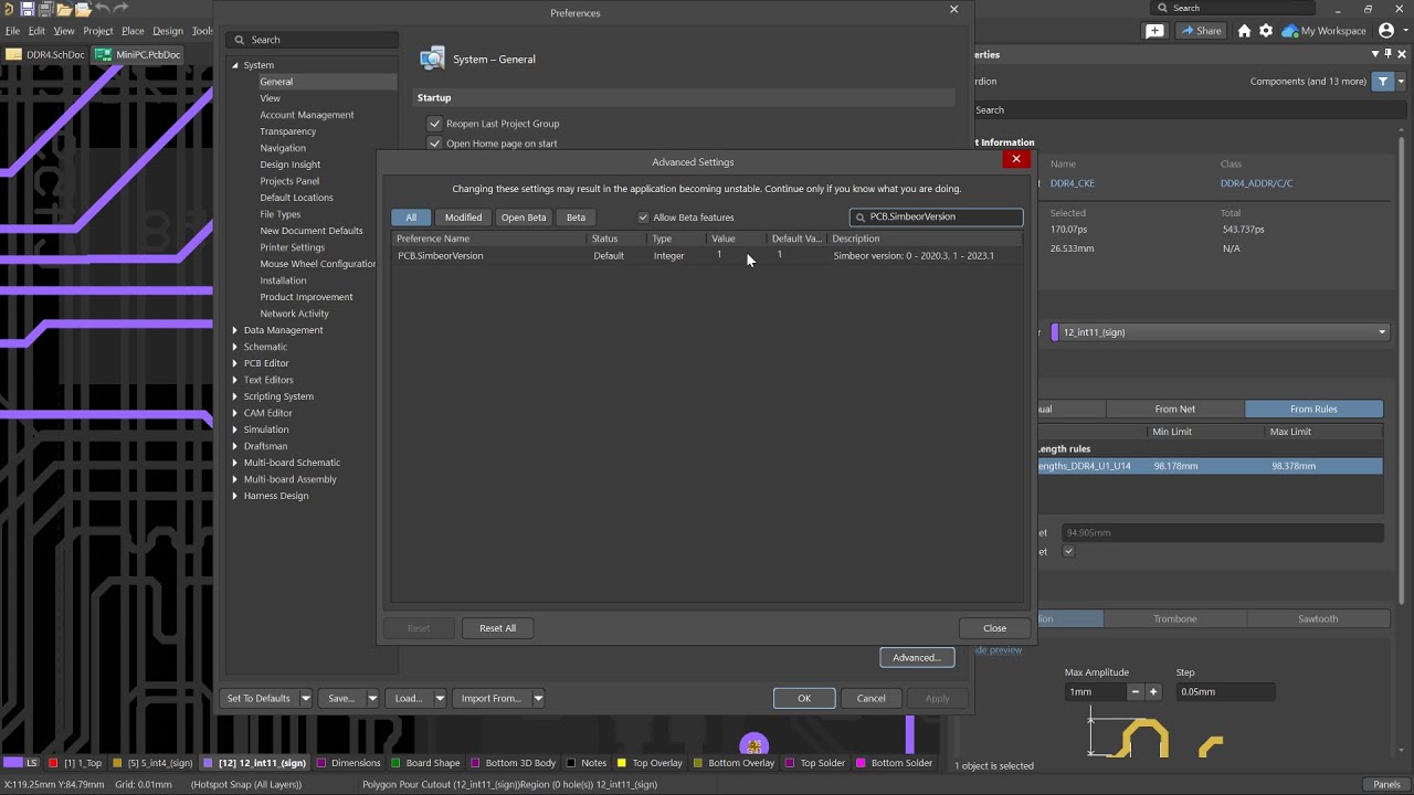
Choose the Simbeor Version for Your PCB Calculations
You can now control which version of Simbeor is used when calculating delay and impedance in the PCB editor.
Recommended Content:
- To learn more about PCB Layout in Altium Designer, visit the resource page.
- Visit the PCB Layout documentation page.
- Learn more about the Octopart Discover, Altium Develop, and Altium Agile platform solutions.
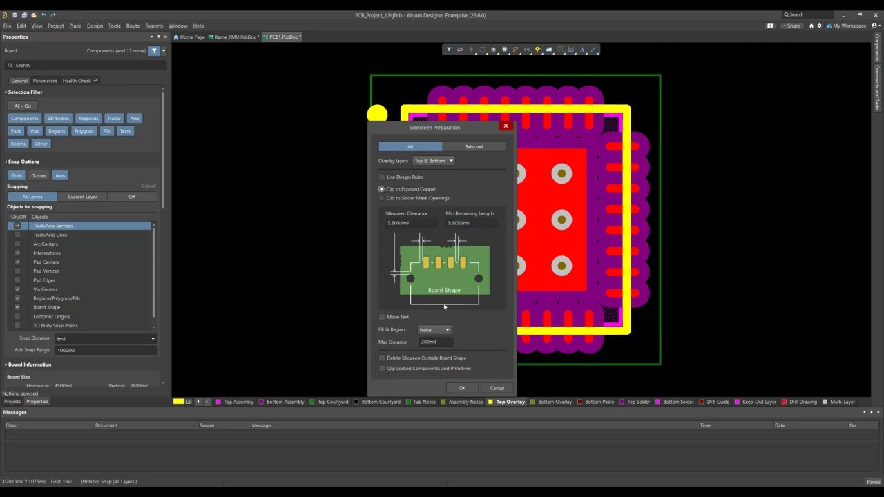
IPC Compliant Footprint Wizard Enhancements
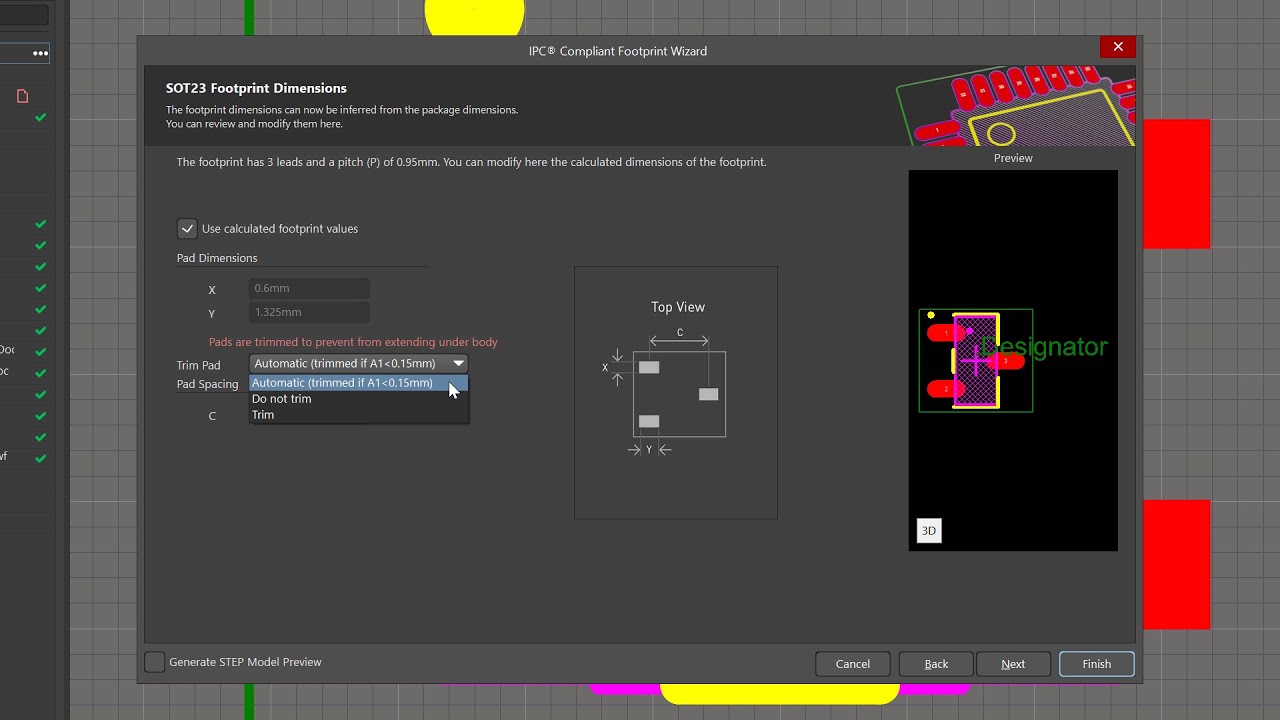
Generate IPC-7351B Compliant Footprints with More Control
The IPC Compliant Footprint Wizard has been updated across supported existing package types to better align generated footprints with IPC-7351B. The update includes changes to footprint calculation, package outline, silkscreen, courtyard, layer mapping, and density table behavior. It also adds pad trimming control for gullwing packages, including support in the batch generator Excel template. Molded package inputs have been clarified with an added lead span range parameter and a renamed body length range parameter.
Recommended Content:
- Learn more about the Octopart Discover, Altium Develop, and Altium Agile platform solutions.
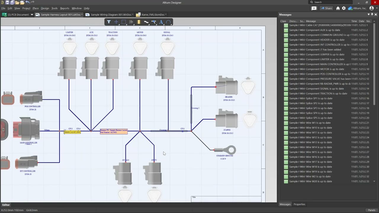
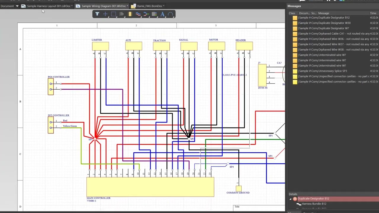
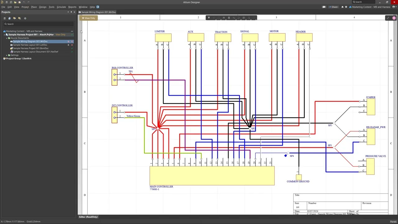
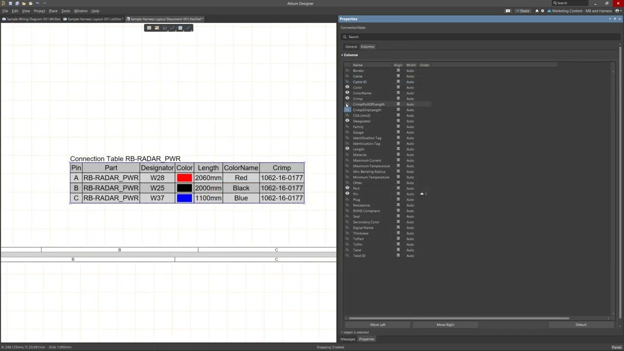
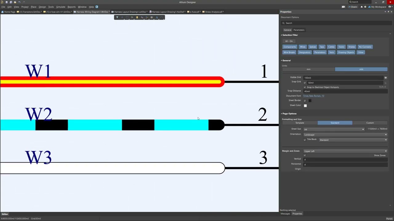
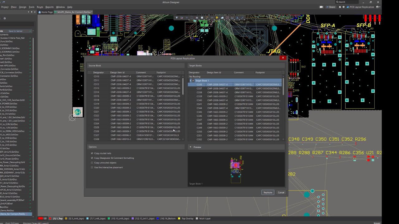
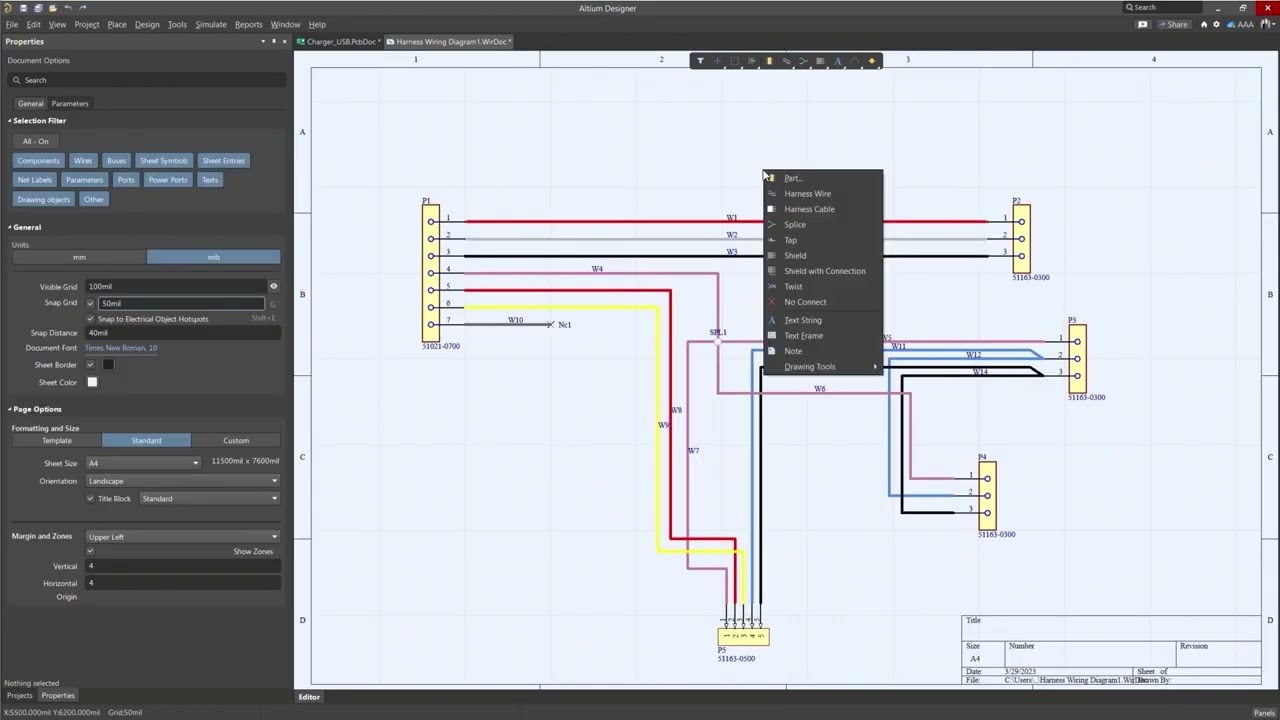
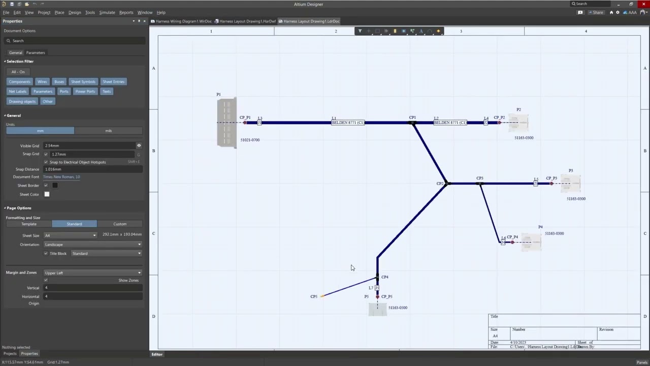
Harness Design Enhancements
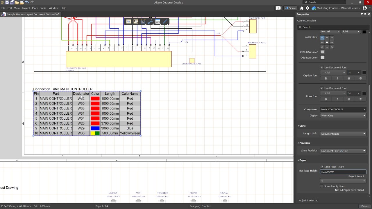
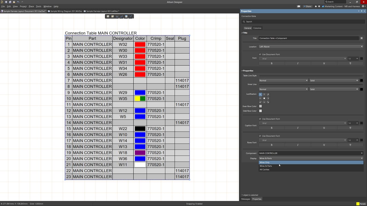
Present Large Harness Tables More Clearly
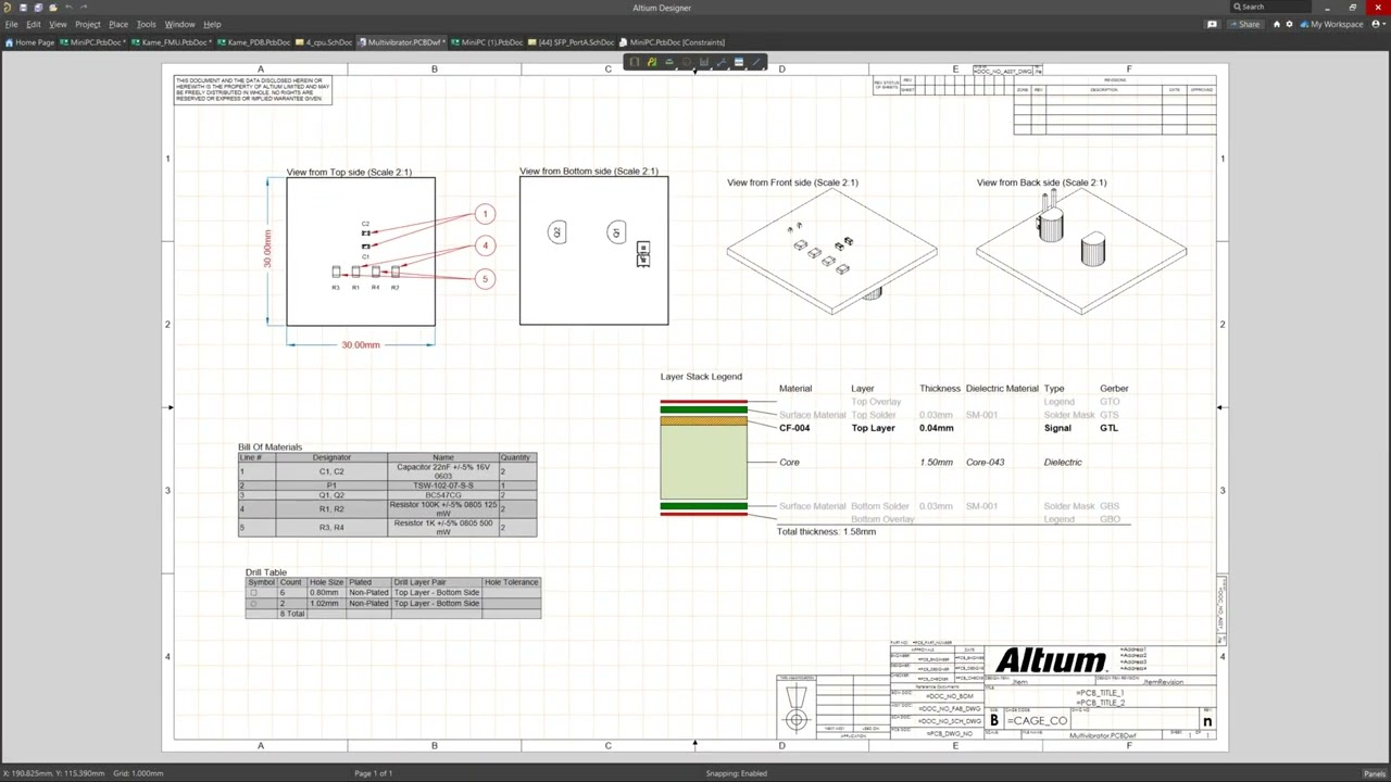
Harness Draftsman now supports splitting a connection table across multiple pages in a *.HarDwf document. A new page height limit lets you control how much of the table is shown on each page. This makes large harness connection tables easier to present in drawings without shrinking the table or moving the data to a separate document.
Recommended Content:
- To see an overview about the Harness Design tool, visit the feature page.
- Visit the Harness Design documentation page.
- Learn more about the Octopart Discover, Altium Develop, and Altium Agile platform solutions.
Component Management Enhancements
Improve Readability with Custom Pin Spacing
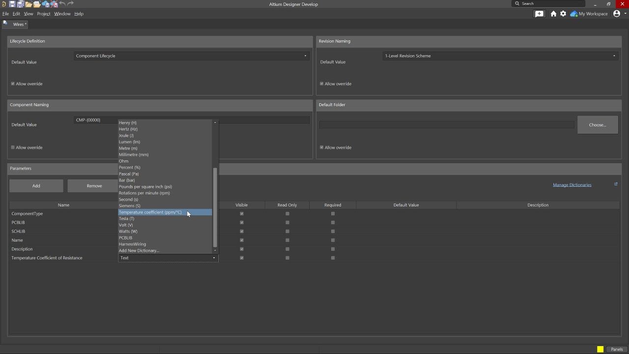
Component templates in a connected Workspace on the Altium Platform now support Temperature coefficient (ppm/°C) as a unit-aware user parameter data type. This allows temperature coefficient values to be defined with the correct units directly in the template.
Recommended Content:
- Learn more about the Octopart Discover, Altium Develop, and Altium Agile platform solutions.
Wire Bonding Enhancements
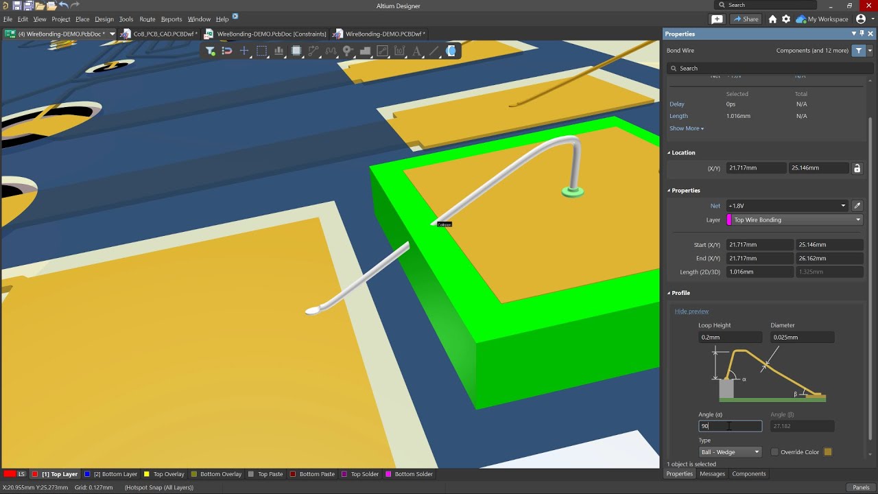
Improve Your 3D Wire Bonding Workflow
Wire bonding design now includes new 3D capabilities for defining bond wire shape, checking clearances, supporting import/export workflows, and managing wire bonding objects.
Recommended Content:
- To see an overview, visit the feature page.
- Learn more about the Octopart Discover, Altium Develop, and Altium Agile platform solutions.
ODB++ Enhancements
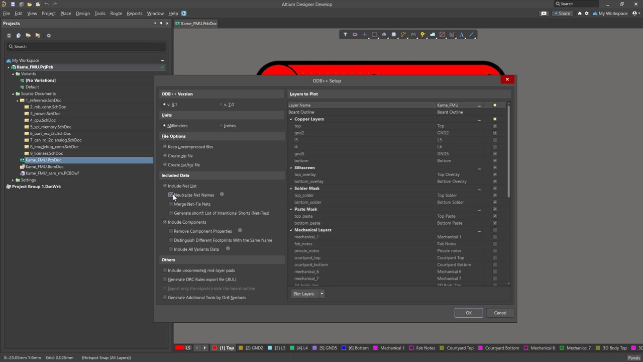
Customize Your ODB++ Output for Each Partner
You can now control exactly what design information is included in ODB++ output for different manufacturing recipients. This includes selecting signal layers for export, choosing whether the netlist is included, disabled, or neutralized, and controlling whether component data is removed or exported without properties.
Recommended Content:
- Visit the fabrication outputs documentation page.
- Learn more about the Octopart Discover, Altium Develop, and Altium Agile platform solutions.
Schematic Capture Enhancements
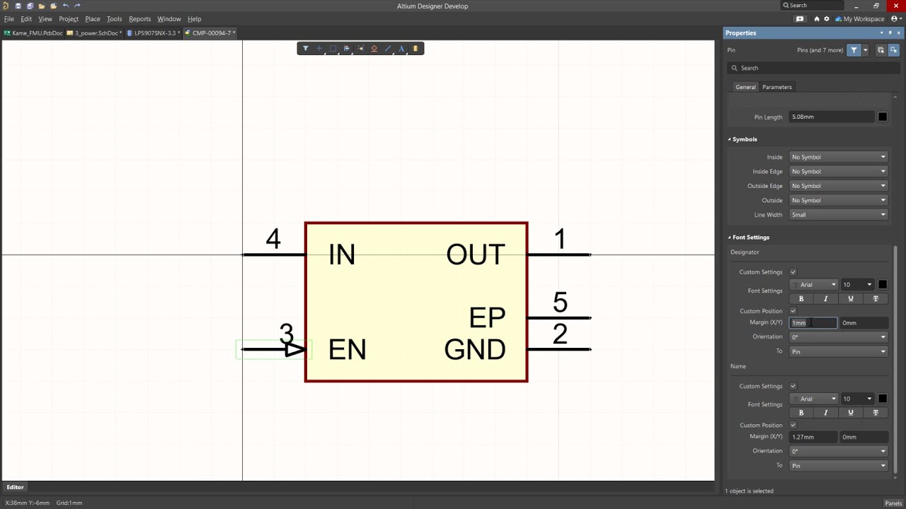
Improve Readability with Custom Pin Spacing
You can now define a custom vertical margin for a pin’s designator and name. This can be configured globally through Schematic Preferences or locally within individual Pin properties.
Recommended Content:
- To learn more about Schematic Capture in Altium Designer, visit the resource page.
- Visit the Schematic Capture documentation page.
- Learn more about the Octopart Discover, Altium Develop, and Altium Agile platform solutions.
PCB Enhancements
Create IPC-Aligned Footprints with Less Effort
The default values for the Solder Mask Expansion rule in PCB documents and rule-driven solder mask expansion in PCB library documents are now set to 0 mil instead of 4 mil.
Recommended Content:
- To learn more about PCB Layout in Altium Designer, visit the resource page.
- Visit the PCB Layout documentation page.
- Learn more about the Octopart Discover, Altium Develop, and Altium Agile platform solutions.
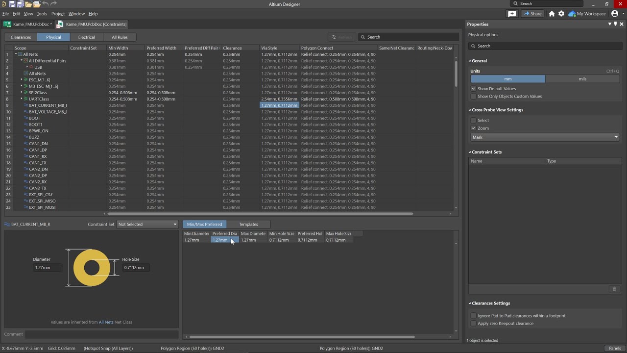
Constraint Manager Enhancements
Make Via Rule Configuration More Intuitive
When defining a routing via style rule in the physical view, you can now specify minimum, maximum, and preferred values for both diameter and hole size. Also, new controls allow you to quickly switch between Min/Max/Preferred constraints and template-based definitions.
Recommended Content:
- To see an overview about the Constraint Manager, visit the feature page.
- Visit the Constraint Manager documentation page.
- Learn more about the Octopart Discover, Altium Develop, and Altium Agile platform solutions.
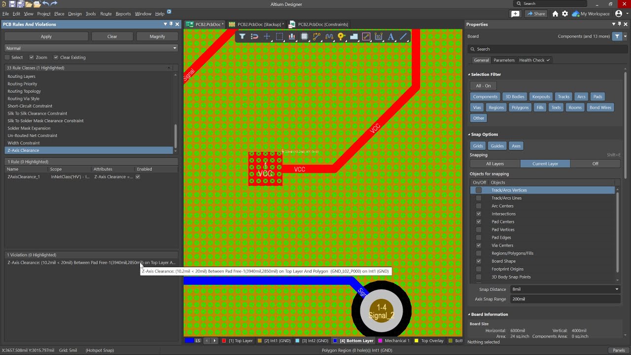
PCB Enhancements
Detect Z-Axis Clearance Issues Earlier
The Z-axis clearance rule allows you to check the shortest distance between copper across layers by defining clearances between specific net classes, differential pairs, or even by applying schematic parameter directives.
Recommended Content:
- To learn more about PCB Layout in Altium Designer, visit the resource page.
- Visit the PCB Layout documentation page.
- Learn more about the Octopart Discover, Altium Develop, and Altium Agile platform solutions.
PCB Enhancements
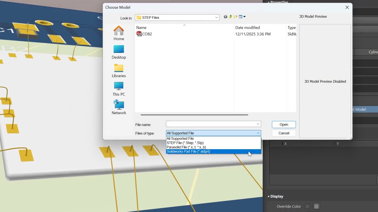
Import and Export with Modern Mechanical Models
We've added support for SOLIDWORKS 2024 and 2025 part models for importing 3D bodies and updated the Parasolid export to version 35.1.
Recommended Content:
- To learn more about PCB Layout in Altium Designer, visit the resource page.
- Visit the PCB Layout documentation page.
- Learn more about the Octopart Discover, Altium Develop, and Altium Agile platform solutions.
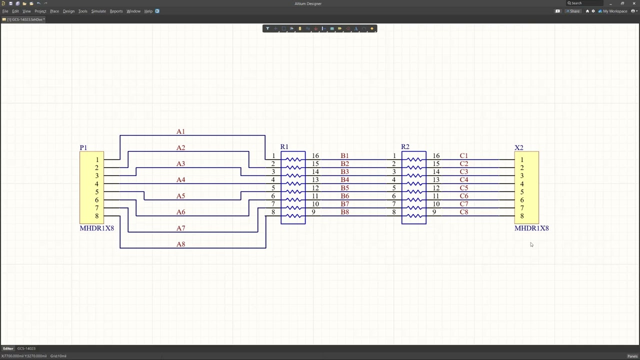
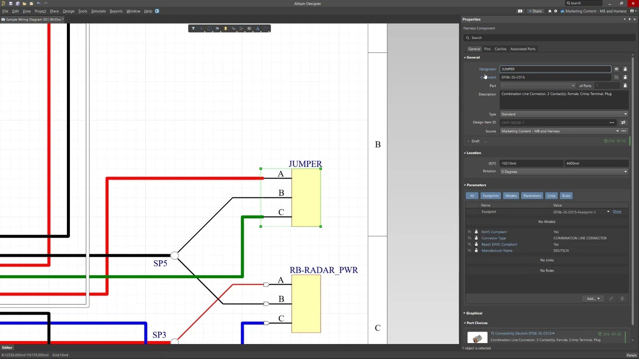
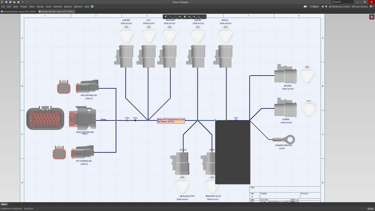
Harness Design Enhancements
Clearly Show Jumper Wires in Your Harness Designs
Jumper wires that connect two cavities within the same connector are now correctly represented in Layout Drawings.
Recommended Content:
- To see an overview about the Harness Design tool, visit the feature page.
- Visit the Harness Design documentation page.
- Learn more about the Octopart Discover, Altium Develop, and Altium Agile platform solutions.
Harness Design Enhancements
Keep Your Harness Designs in Sync with Library Updates
The "Update From Libraries" feature is expanded to support more harness-related objects in Wiring Diagrams and Layout Drawings.
Recommended Content:
- To see an overview about the Harness Design tool, visit the feature page.
- Visit the Harness Design documentation page.
- Learn more about the Octopart Discover, Altium Develop, and Altium Agile platform solutions.
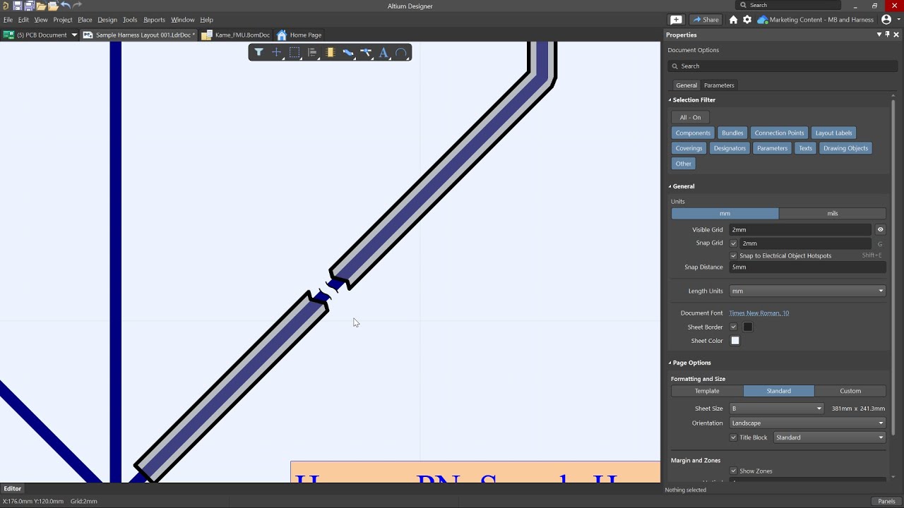
Harness Design Enhancements
Clearly Communicate Your True Harness Length
The harness bundle length is now automatically set to match the drawn length in the layout, and when you enter the real physical length and it is different, Altium Designer clearly marks the bundle with a 'Not to Scale' break symbol. Also, when a covering extends over a bundle with a break symbol, a corresponding break symbol will be displayed for that covering.
Recommended Content:
- To see an overview about the Harness Design tool, visit the feature page.
- Visit the Harness Design documentation page.
- Learn more about the Octopart Discover, Altium Develop, and Altium Agile platform solutions.
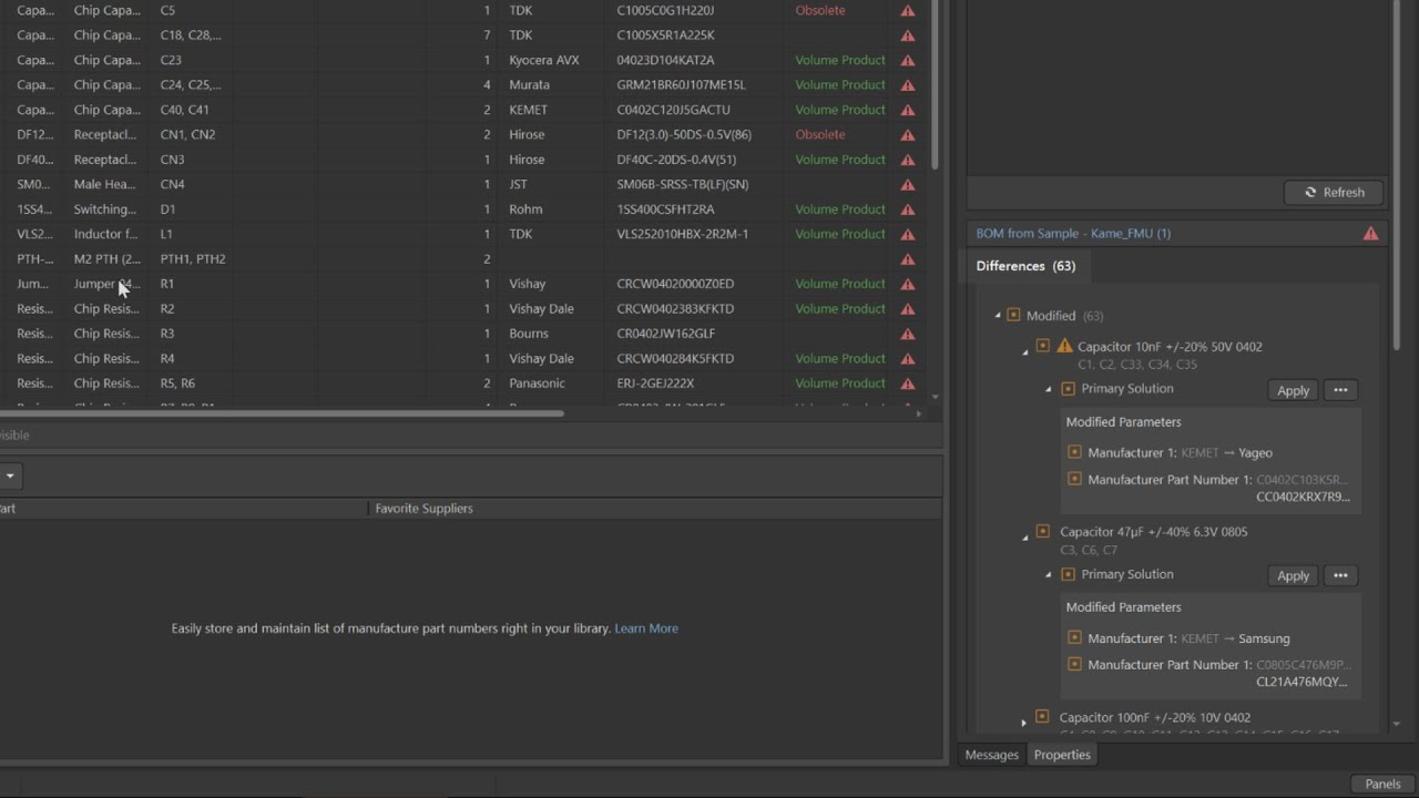
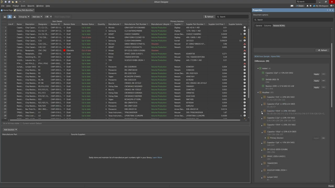
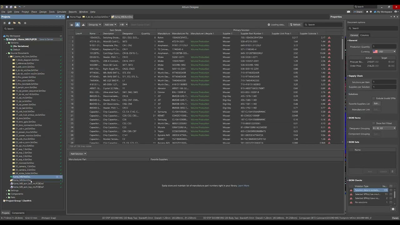
BOM CoDesign Enhancements
Save Time Looking at Differences in BOM CoDesign
You can now automatically exclude supplier related data from the differences section when comparing the engineering activeBOM with procurement BOMs managed in the BOM portal using BOM CoDesign.
Recommended Content:
- Visit the BOM CoDesign documentation page.
- Learn more about the Octopart Discover, Altium Develop, and Altium Agile platform solutions.
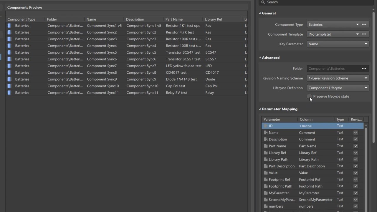
Component Management Enhancements
Protect Component Lifecycle States During Synchronization
A new Preserve lifecycle state option allows you to keep the existing lifecycle state when synchronizing components between your Workspace and your component database using the Components Synchronization feature.
Recommended Content:
- Learn more about the Octopart Discover, Altium Develop, and Altium Agile platform solutions.
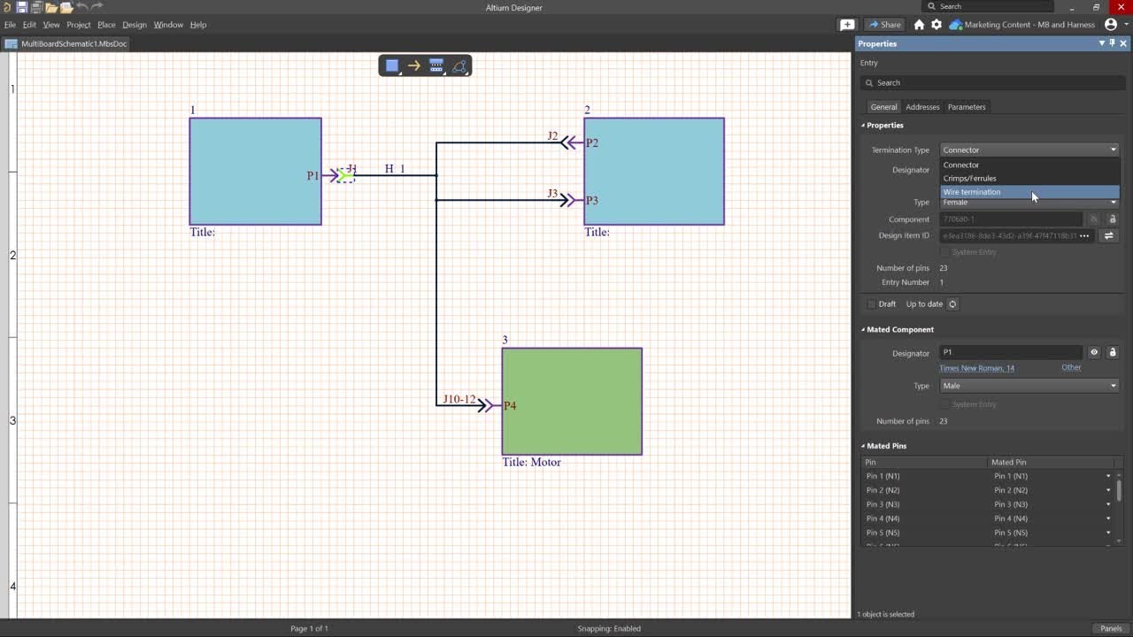
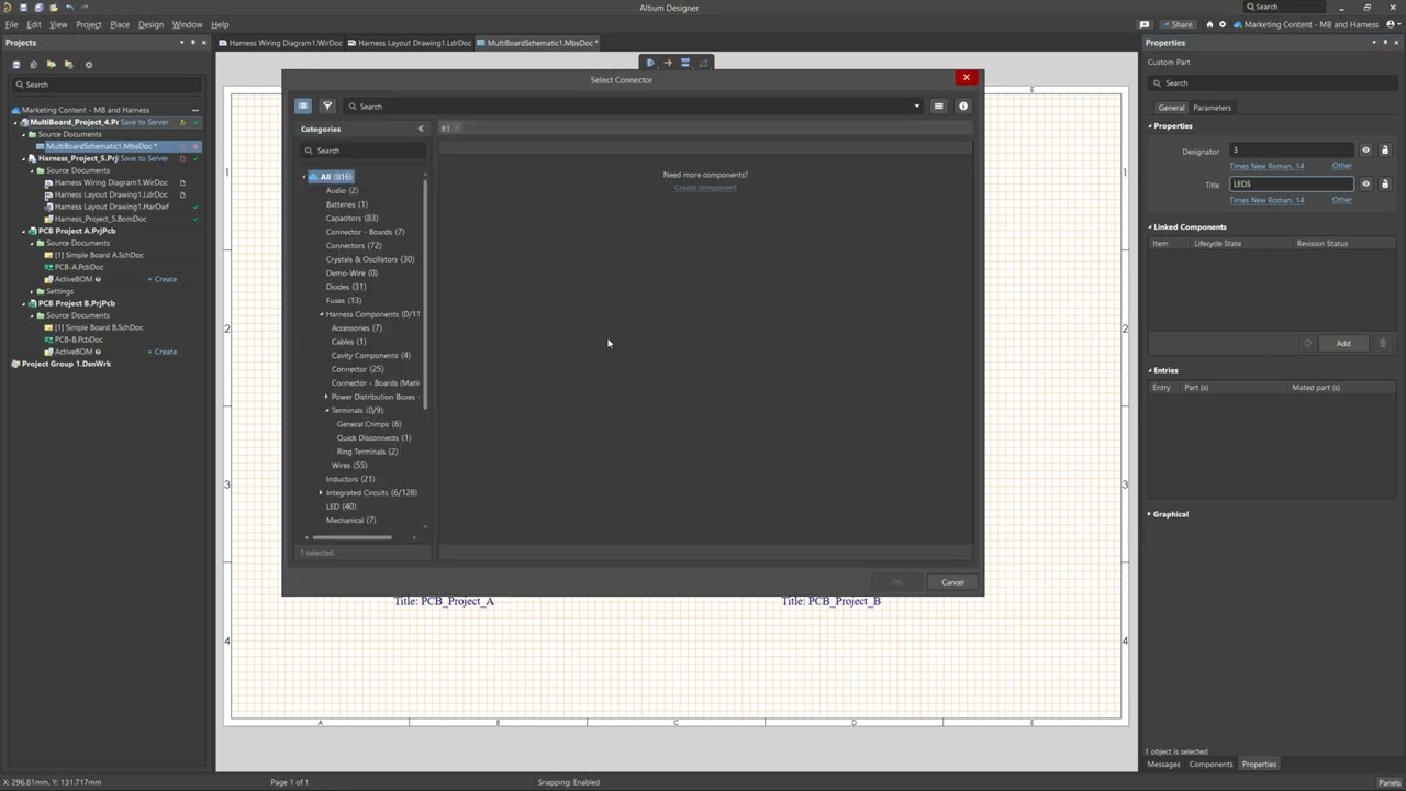
Multi-board Design Enhancements
Define Your Multi-board Terminations with Precision
You can now define termination types directly in your multi-board schematics, with the ability to clearly specify if each harness entry connects to a connector, a crimp or ferrule, or a simple wire termination, giving you precise control over every connection.
Recommended Content:
- To see an overview visit the Multi-board Design feature page.
- Visit the Multi-board Design documentation page.
- Learn more about the Octopart Discover, Altium Develop, and Altium Agile platform solutions.
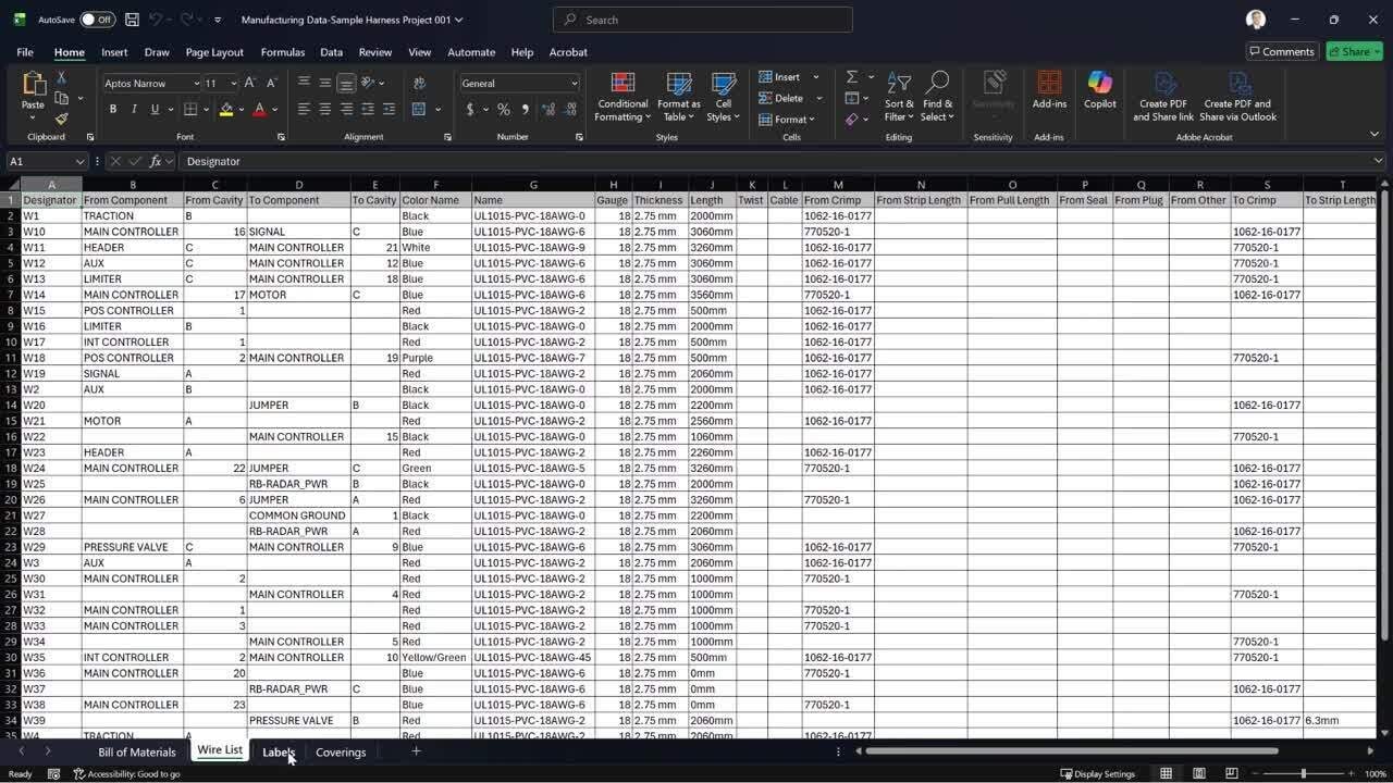
Harness Design Enhancements
Export a Complete Harness Excel Manufacturing Workbook
You can export a complete Excel manufacturing workbook directly from your project This includes your BOM for quoting, wiring lists for automation, label summaries, and detailed covering information for assembly. Enhancements also include smarter wire validation, more flexible covering control, and clearer “As Required” material reporting for a smoother, more accurate manufacturing workflow.
Recommended Content:
- To see an overview about the Harness Design tool, visit the feature page.
- Visit the Harness Design documentation page.
- Learn more about the Octopart Discover, Altium Develop, and Altium Agile platform solutions.
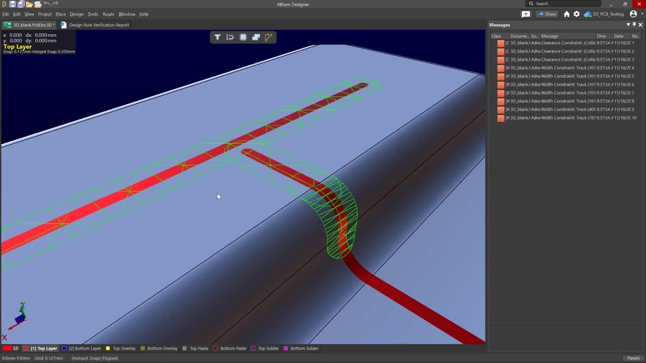
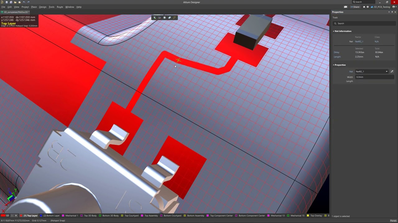
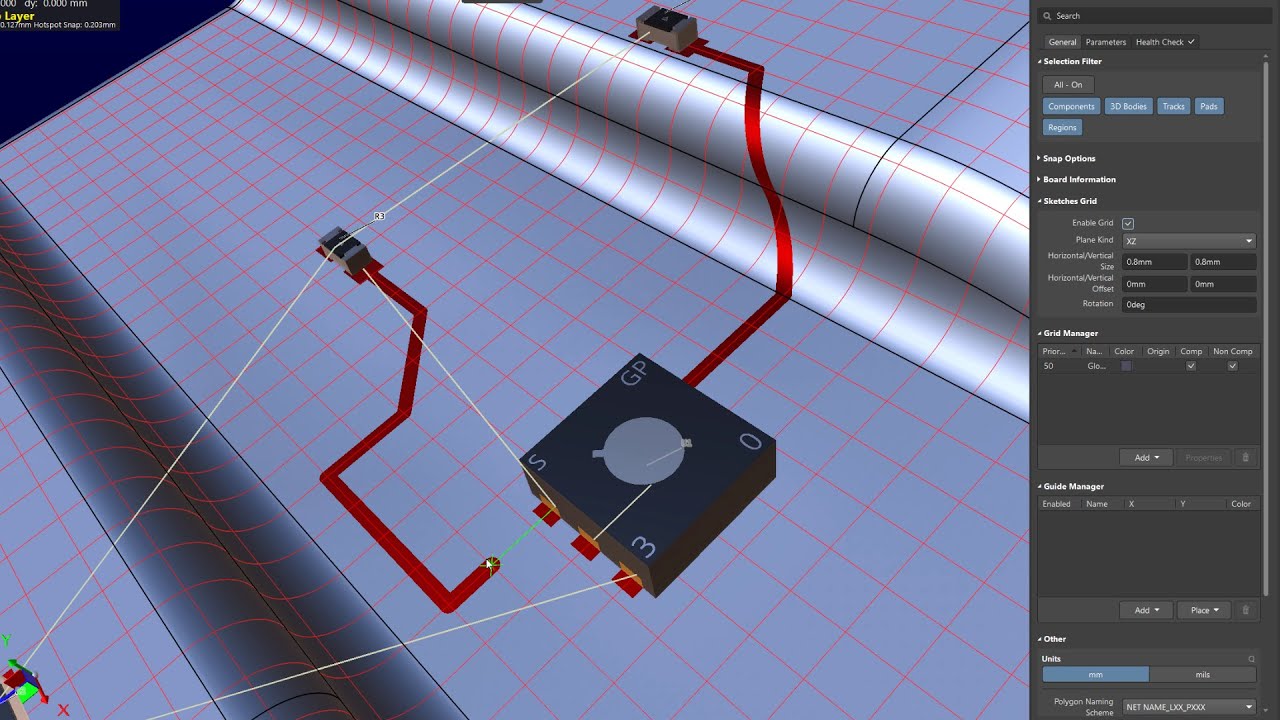
3D-MID Enhancements
Validate Your 3D-MID Designs with Confidence
You can now run batch design rule checking for width, clearance, length, and matched lengths violations on all routed tracks on your 3D substrate.
Recommended Content:
- To see an overview about the 3D-MID Design Tool, visit the feature page.
- Visit the 3D-MID Design documentation page.
- Learn more about the Octopart Discover, Altium Develop, and Altium Agile platform solutions.
Altium Designer 25
Constraint Manager Enhancements
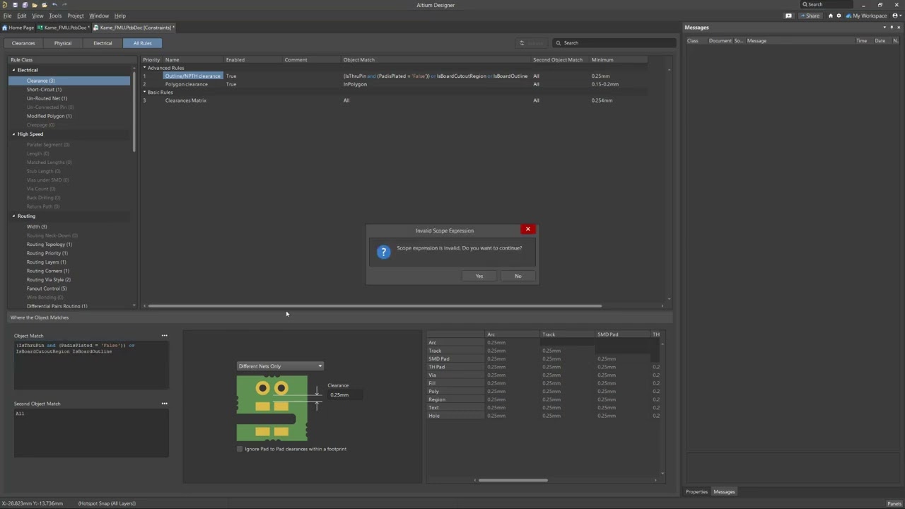
Catch Your Syntax Issues Early for Custom Rules
The Constraint Manager now automatically detects and highlights any rule containing a syntactically incorrect custom query expression.
Recommended Content:
- To see an overview about the Constraint Manager, visit the feature page.
- Check out our recent OnTrack Podcast video on the Constraint Manager, Deep Diving Into Altium Designer's New Constraint Manager.
- Visit the Constraint Manager documentation page.
Multi-board Design Enhancements
Enhance Your Modular Design with Inline Harness Connectors
The Inline Harness Connector feature in the multi-board schematic editor now allows you to divide an existing harness connection into two parts.
Recommended Content:
- To see an overview visit the Multi-board Design feature page.
- Check out our recent webinar on system design, Unlock Complete System Design with Altium Designer 24.
- Visit the Multi-board Design documentation page.
Harness Design Enhancements
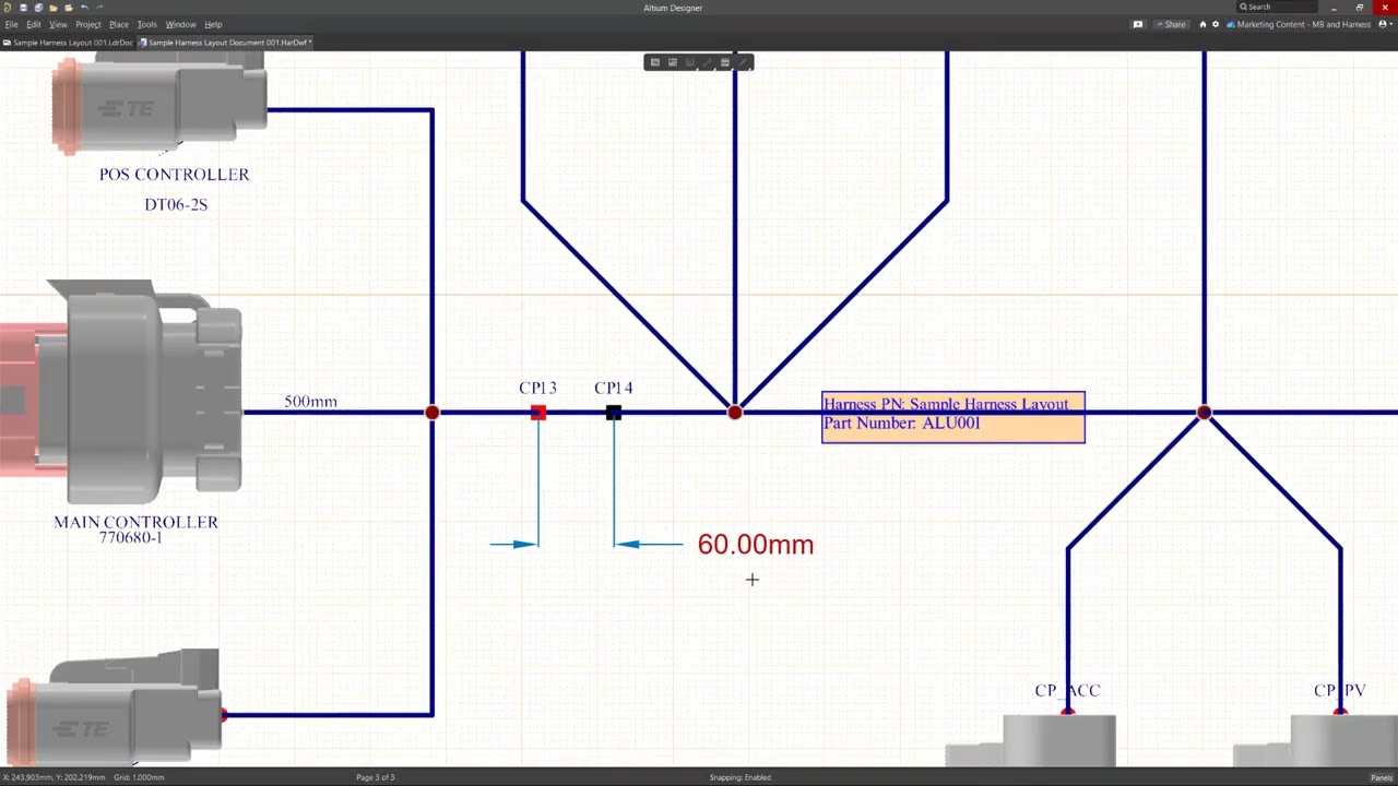
Speed Up Your Harness Drafting with Automatic Length Fills
The value field now automatically populates with the corresponding bundle length when you place a linear dimension between connection points in a harness manufacturing drawing.
Recommended Content:
- To see an overview about the Harness Design tool, visit the feature page.
- Check out our recent webinar on Harness Design, Future-Proof your Wire Harnesses with Altium Designer.
- Visit the Harness Design documentation page.
Constraint Manager Enhancements
Boost Your Productivity with Automated Constraint Manager Refreshes
The Constraint Manager now automatically refreshes to import schematic directives when you push changes to the PCB using the Engineering Change Order (ECO) process.
Recommended Content:
- To see an overview about the Constraint Manager, visit the feature page.
- Check out our recent OnTrack Podcast video on the Constraint Manager, Deep Diving Into Altium Designer's New Constraint Manager.
- Visit the Constraint Manager documentation page.
Multi-board Design Enhancements
Accelerate Your Multi-Board Design with Collaborative Features
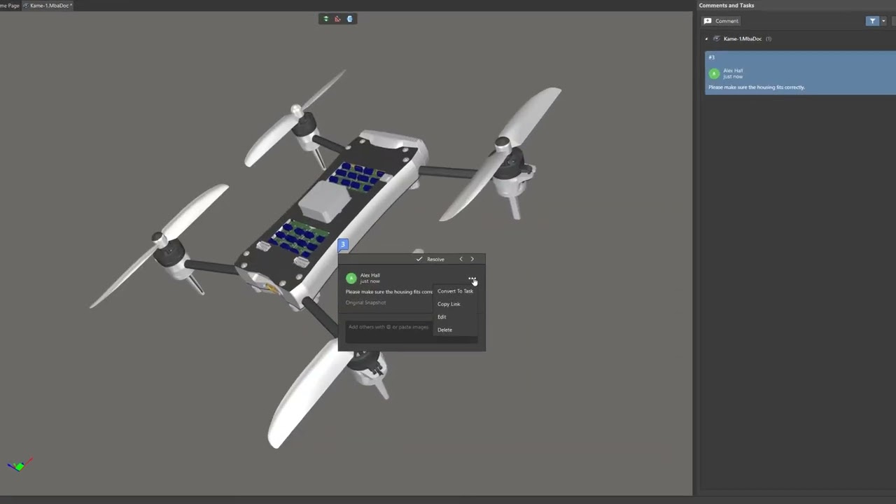
There is now support for interactive commenting and task management in Multi-board Assembly documents.
Recommended Content:
- To see an overview visit the Multi-board Design feature page.
- Check out our recent webinar on system design, Unlock Complete System Design with Altium Designer 24.
- Visit the Multi-board Design documentation page.
Component Management Enhancements
Simplify Your Workflow Through Grouped Component Operations
All components are now organized under a new ‘Workspace Components’ folder in the Projects panel. This allows you to open, close, save locally, push to the Workspace, or discard changes for all grouped components at once.
Constraint Manager Enhancements
Quickly Recover Your Edits in the Constraint Manager
You now have the ability to Undo/Redo changes made within the Constraint Manager.
Recommended Content:
- To see an overview about the Constraint Manager, visit the feature page.
- Visit the Constraint Manager documentation page.
Harness Design Enhancements
Enhance Your Harness Design Accuracy and Visualization
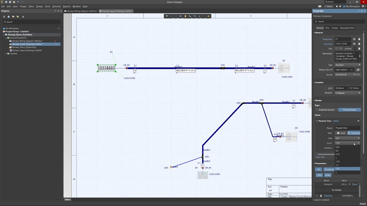
Parasolid format 3D models are now embedded in the layout drawing when adding a Physical View for a harness component or connection point.
Recommended Content:
- To see an overview about the Harness Design tool, visit the feature page.
- Check out our recent webinar on Harness Design, Future-Proof your Wire Harnesses with Altium Designer.
- Visit the Harness Design documentation page.
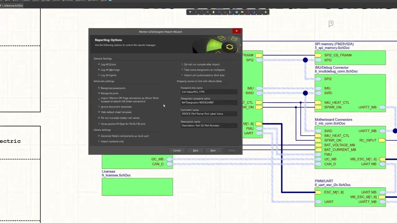
Importer Enhancements
Import Your Designs Seamlessly from Third-Party Tools
When importing an xDX Designer design, a new option has been added that allows you to import 'off-page' connectors in the source design as ports on the generated schematic documents, rather than default off-sheet connectors.
Recommended Content:
- Visit the Import/Export documentation page to learn more.
Constraint Manager Enhancements
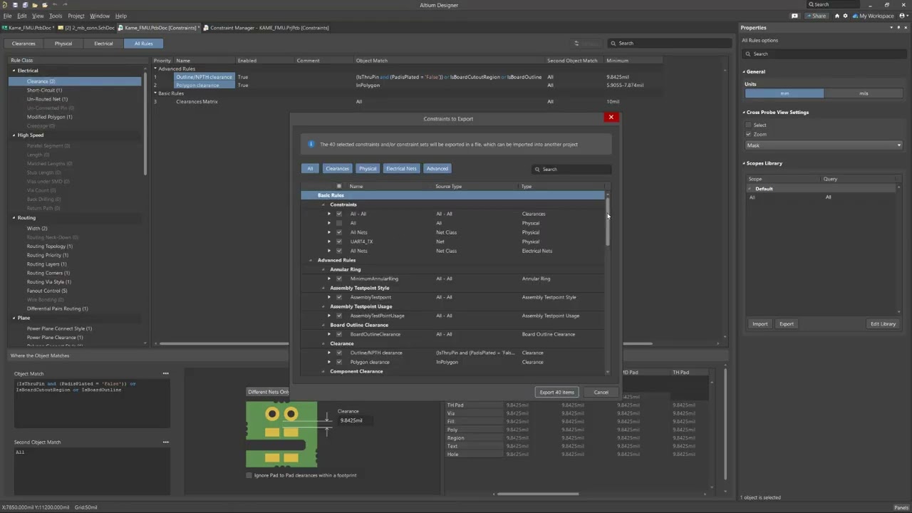
Easily Synchronize Your Design Rules Across Projects
Advanced Rules with custom scopes can now be imported and exported from the Constraint Manager in Altium Designer. With this upgrade, all design rules can now be exported and imported using this functionality.
Recommended Content:
- To see an overview about the Constraint Manager, visit the feature page.
- Visit the Constraint Manager documentation page.
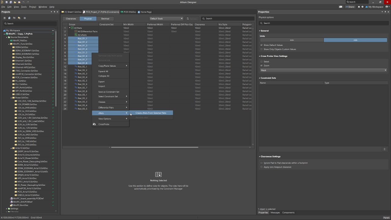
Constraint Manager Enhancements
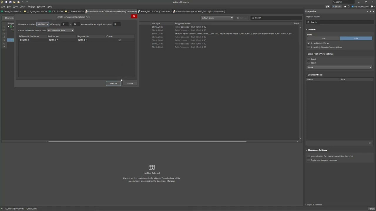
Efficiently Generate Your Differential Pairs from xNets
Differential pairs can now be generated from xNets using either the Physical view or the Diff Pairs tab of the Electrical view in the Constraint Manager.
Recommended Content:
- To see an overview about the Constraint Manager, visit the feature page.
- Visit the Constraint Manager documentation page.
Harness Design Enhancements
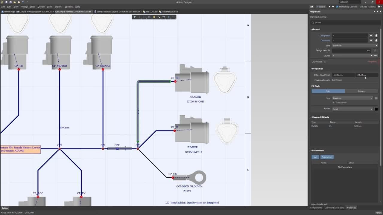
Achieve Greater Precision for Your Harness Coverings
The Start offset and End offset can now be specified for a harness covering, which, combined with the enclosed bundle segment length, automatically calculates and displays the accurate covering length directly in the main design space and the BOM.
Recommended Content:
- To see an overview about the Harness Design tool, visit the feature page.
- Visit the Harness Design documentation page.
Constraint Manager Enhancements
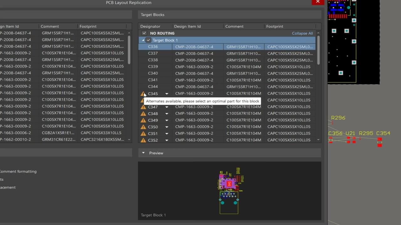
Simplify Routing with Automated Custom Topology and xSignal Creation
The Constraint Manager now automatically creates custom routing topologies and xSignals for xNets that traverse discrete components with more than two pins, such as resistor banks, upon selecting the Custom routing topology type.
Recommended Content:
- To see an overview about the Constraint Manager, visit the feature page.
- Visit the Constraint Manager documentation page.
Harness Design Improvements
Ensure Comprehensive Documentation in Your Harness Designs
In harness design, we’ve added the ability to specify Strip Length and Pull Off Length for pins lacking an assigned cavity type.
Recommended Content:
- To see an overview about the Harness Design tool, visit the feature page.
- Check out our recent webinar on Harness Design, Future-Proof your Wire Harnesses with Altium Designer.
- Visit the Harness Design documentation page.
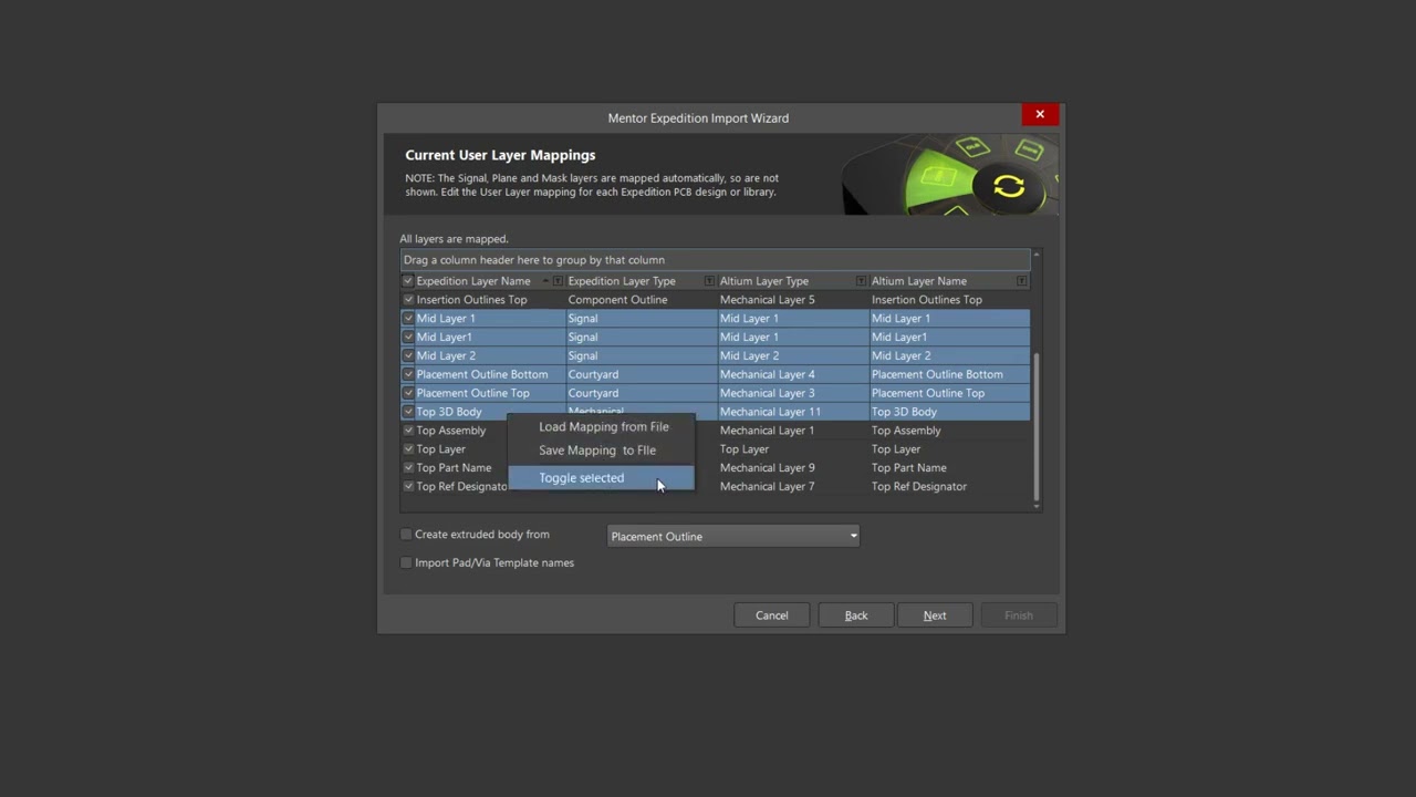
Importer Enhancements
Efficiently Manage Layers When Importing Xpedition Files
The import process for Mentor Xpedition files has been enhanced to allow toggling multiple layers on or off simultaneously during import.
Recommended Content:
- Visit the Import/Export documentation page to learn more.
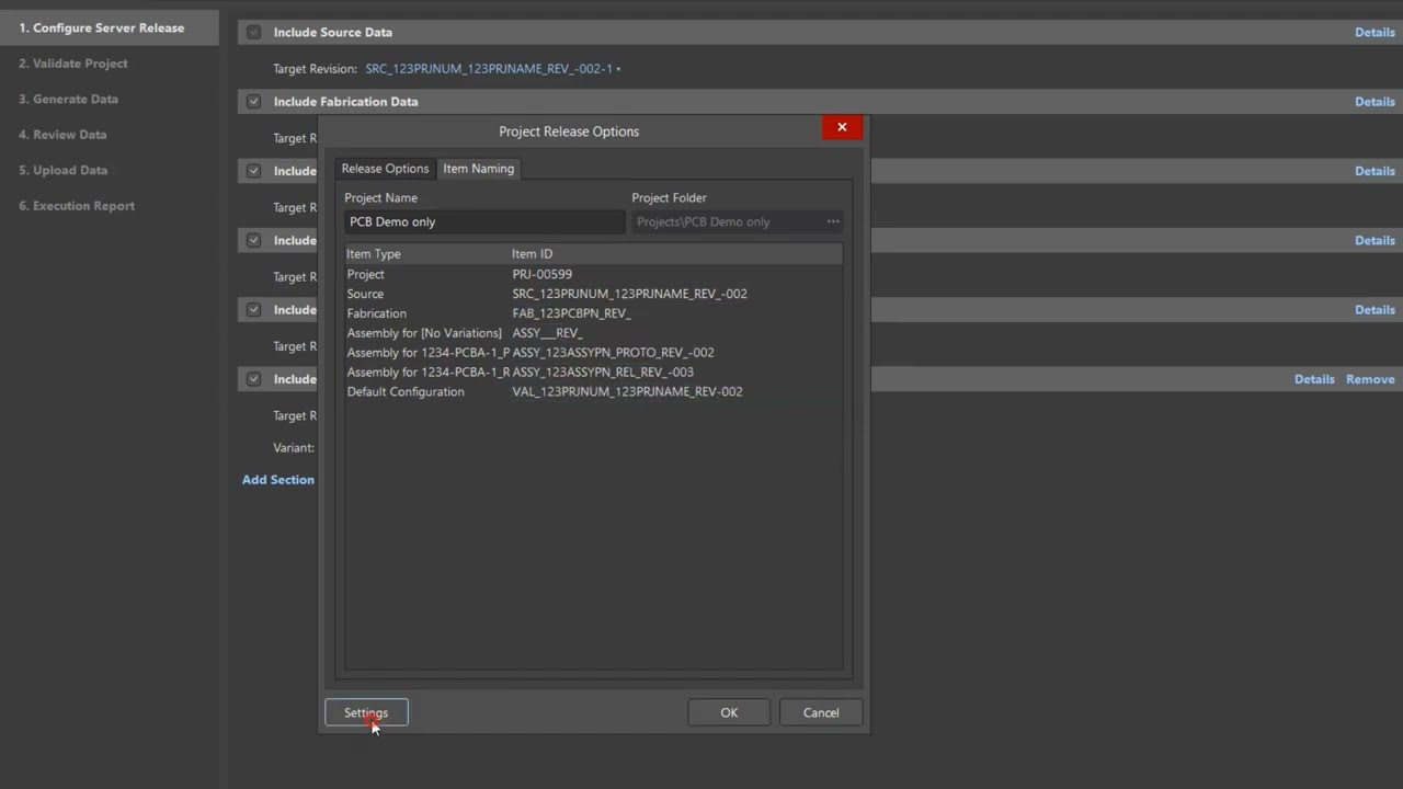
Design Output Improvements
Improve Organization and Accuracy Across Project Release Data
Defined project and variant parameters from your connected Workspace templates are now accurately used in naming released data sets such as Source, Fabrication, Assembly, and Custom outputs.
Recommended Content:
- Visit the Preparing Outputs and Releasing the Project documentation page to learn more.
Constraint Manager Enhancements
Import Clearance Rules Automatically into the Clearance Matrix
When importing clearance rules from schematic design directives or migrating projects from the legacy design rules dialog, clearance rules are now placed in the Clearance Matrix within the Constraint Manager, rather than being assigned to the Advanced Rules section.
Recommended Content:
- To see an overview about the Constraint Manager, visit the feature page.
- Check out our recent OnTrack Podcast video on the Constraint Manager, Deep Diving Into Altium Designer's New Constraint Manager.
- Visit the Constraint Manager documentation page.
Harness Design Improvements
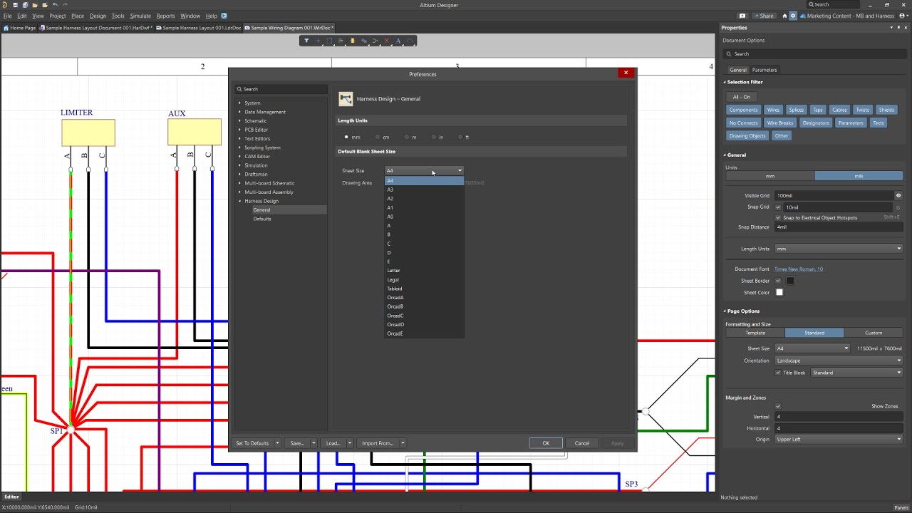
Gain More Control Over Your Harness Design Settings
You now have more control over harness design settings. A new preference lets you set the default blank sheet size for wiring diagrams and layout drawings. Length units have been standardized and can be customized at different levels, including preferences, documents, and tables like BOMs and connection lists. You can also filter connection tables to show only 'no connect' objects. Additionally, a fix ensures that specified units now apply correctly to all wires, including those not part of a cable.
Recommended Content:
- To see an overview about the Harness Design tool, visit the feature page.
- Check out our recent webinar on Harness Design, Future-Proof your Wire Harnesses with Altium Designer.
- Visit the Harness Design documentation page to learn more.
PCB Layout Enhancements
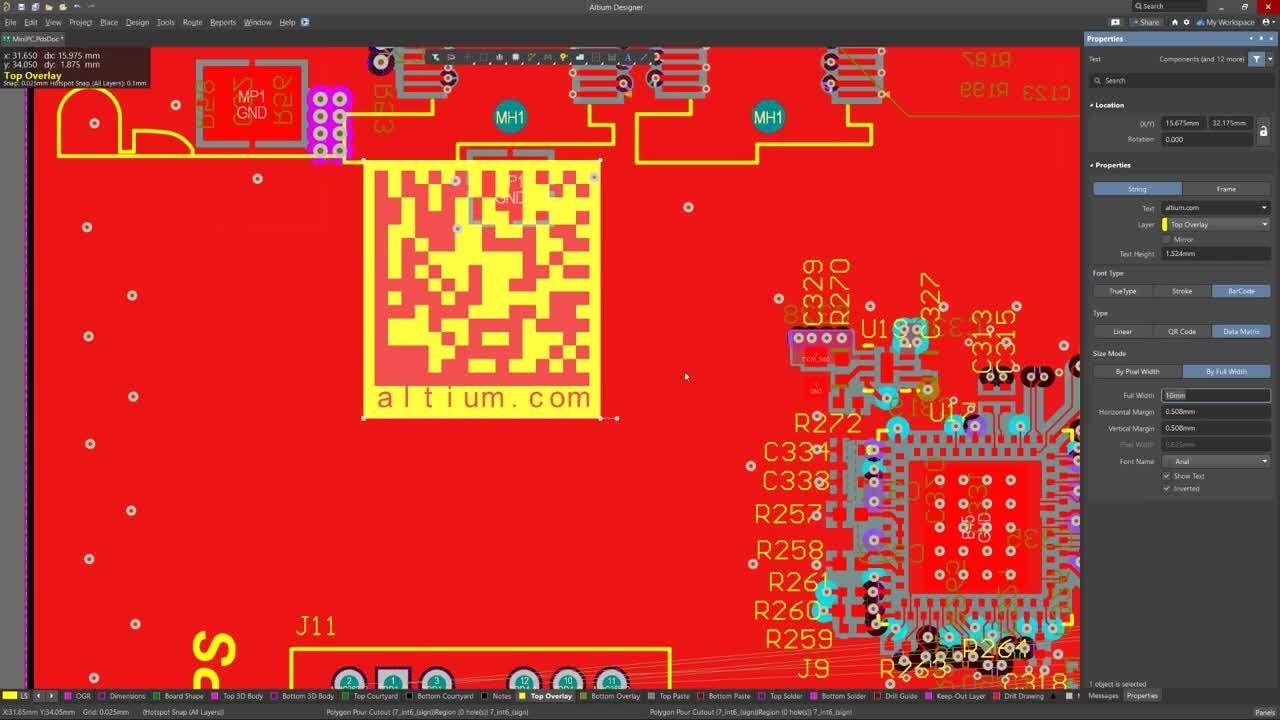
Generate and Place QR and Data Matrix Codes on your PCB
You can now generate and place QR and Data Matrix codes directly in your PCB design, making it easier to add scannable data for tracking, identification, and automation.
Recommended Content:
- To learn more about PCB Layout in Altium Designer, visit the resource page.
- Visit the PCB Layout documentation page.
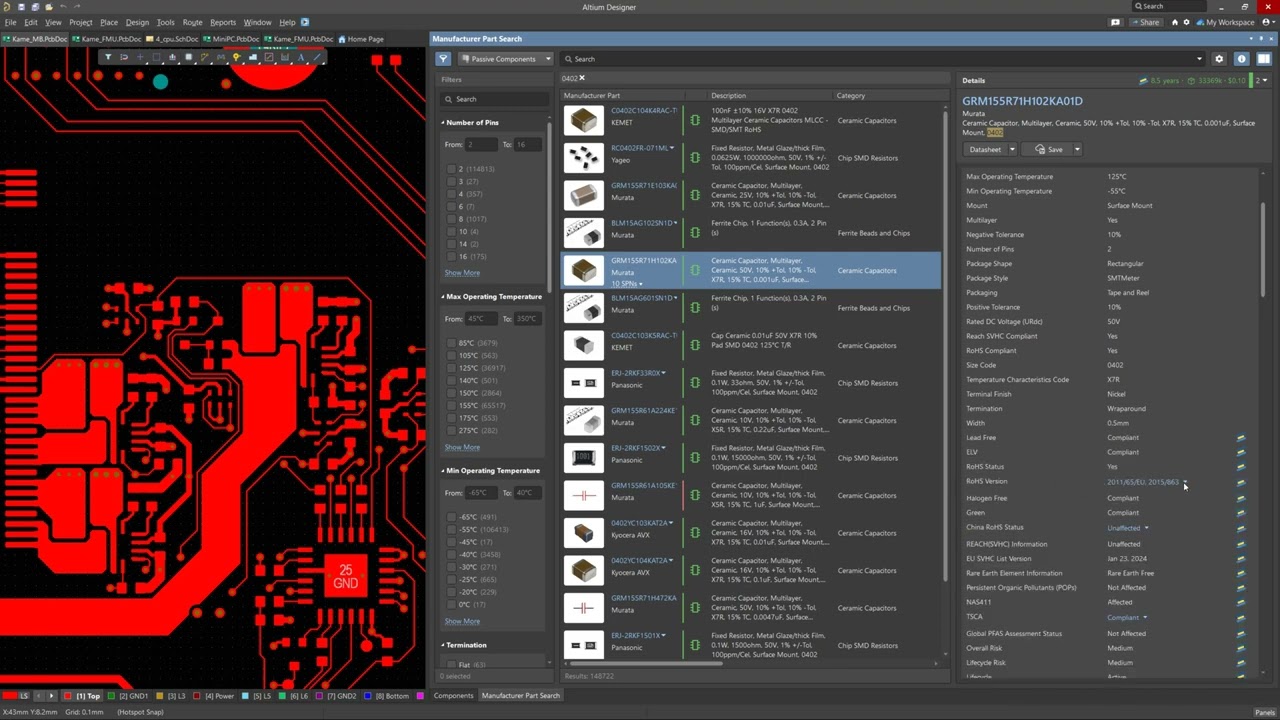
Component Management Enhancements
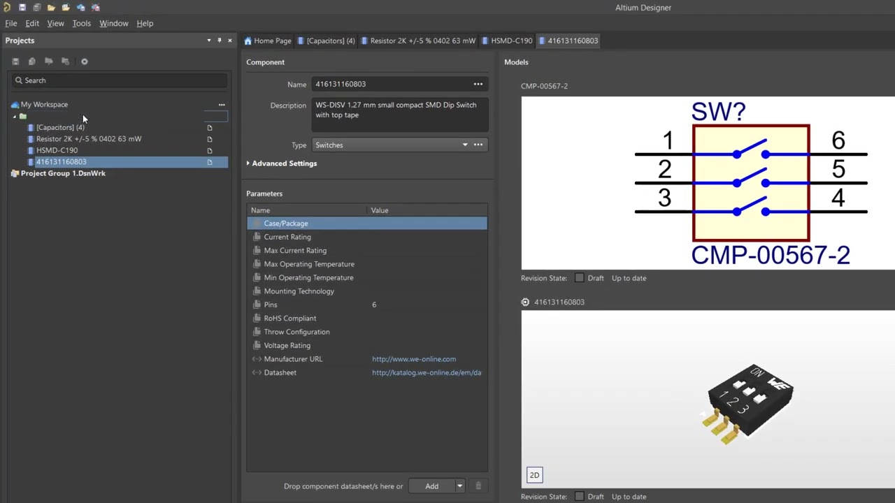
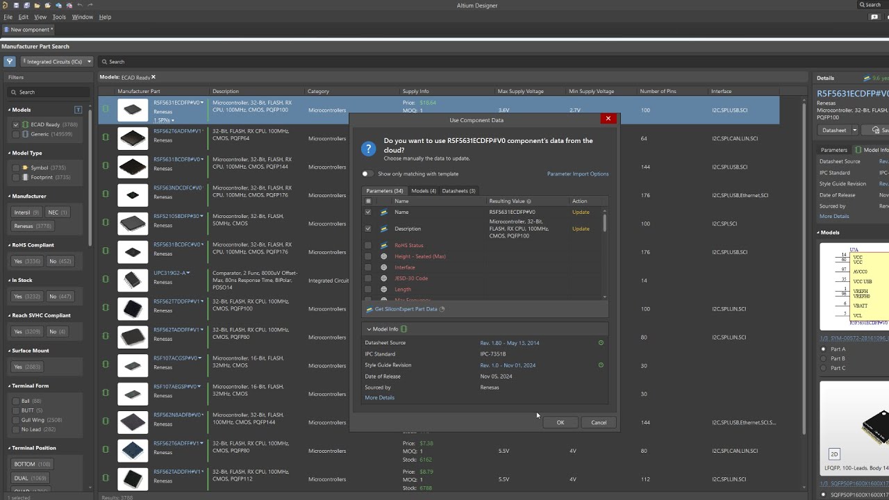
Use Qualified Models and Access Detailed Part Information
Categorizes part models as 'Generic' or 'ECAD Ready,' with detailed model information available in the Manufacturer Part Search panel and related dialogs.
Recommended Content:
- Visit the Component Management documentation page to learn more.
Constraint Manager Enhancements
Make Automated xNets for Serial Component Pin Configurations
Enhanced xNet generation for serial components automates the creation of xNets in the Constraint Manager based on the pin configurations of components, supporting dual-inline, single-inline, and odd-pin configurations.
Recommended Content:
- To see an overview about the Constraint Manager, visit the feature page.
- Check out our recent OnTrack Podcast video on the Constraint Manager, Deep Diving Into Altium Designer's New Constraint Manager.
- Visit the Constraint Manager documentation page.
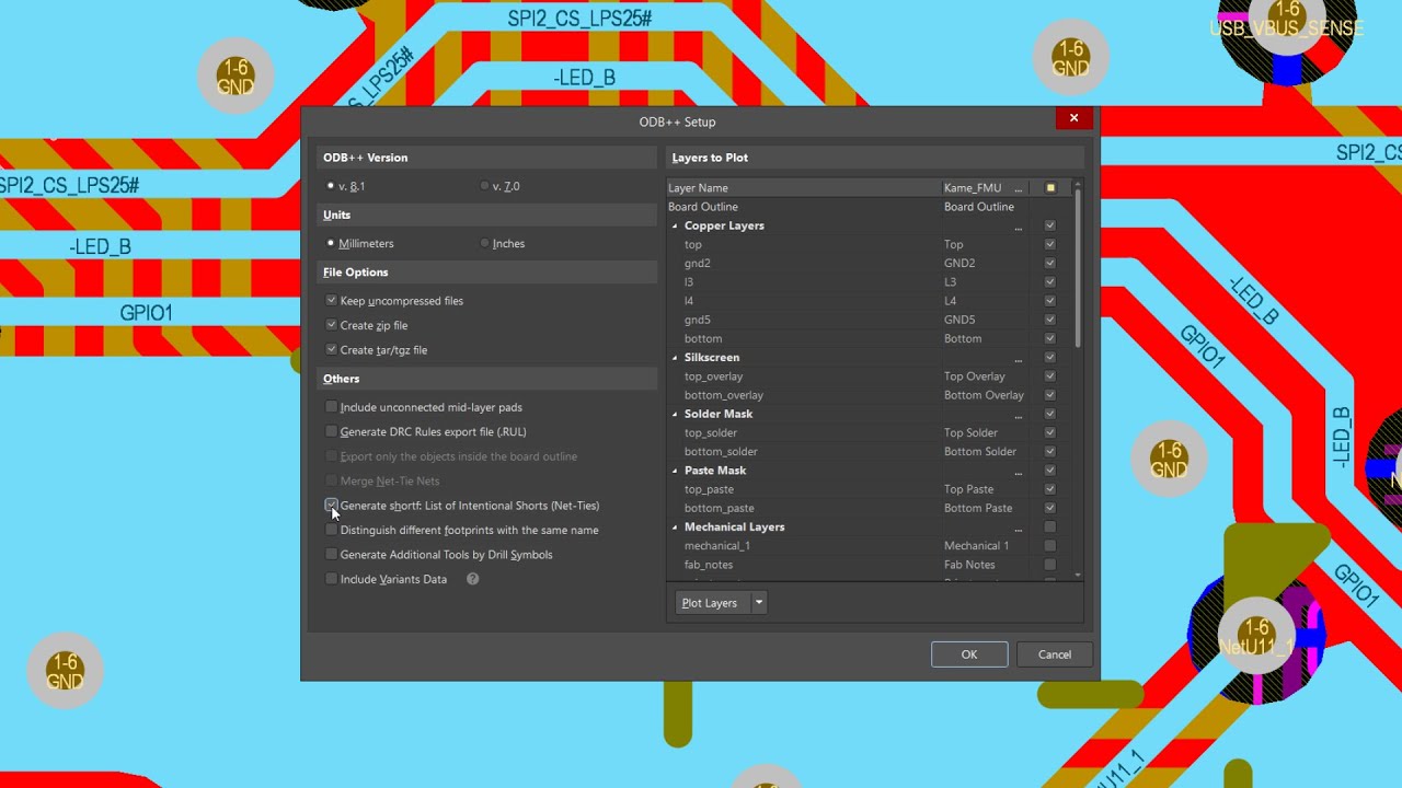
ODB++ Enhancements
Generate an Intentional Shorts List with ODB++ v8.1 Support
Adds support for generating a list of intentional shorts (Net-Ties) in ODB++ v8.1 output, including a new option in the ODB++ Setup dialog.
BOM CoDesign Feature
Enable Collaborative BOM Management with BOM CoDesign
Through the Altium 365 Workspace, designers and procurement specialists can collaborate on related BOM snapshots, allowing for detailed comparisons between managed BOMs and the design’s ActiveBOM.
Recommended Content:
- Visit the BOM CoDesign documentation page.
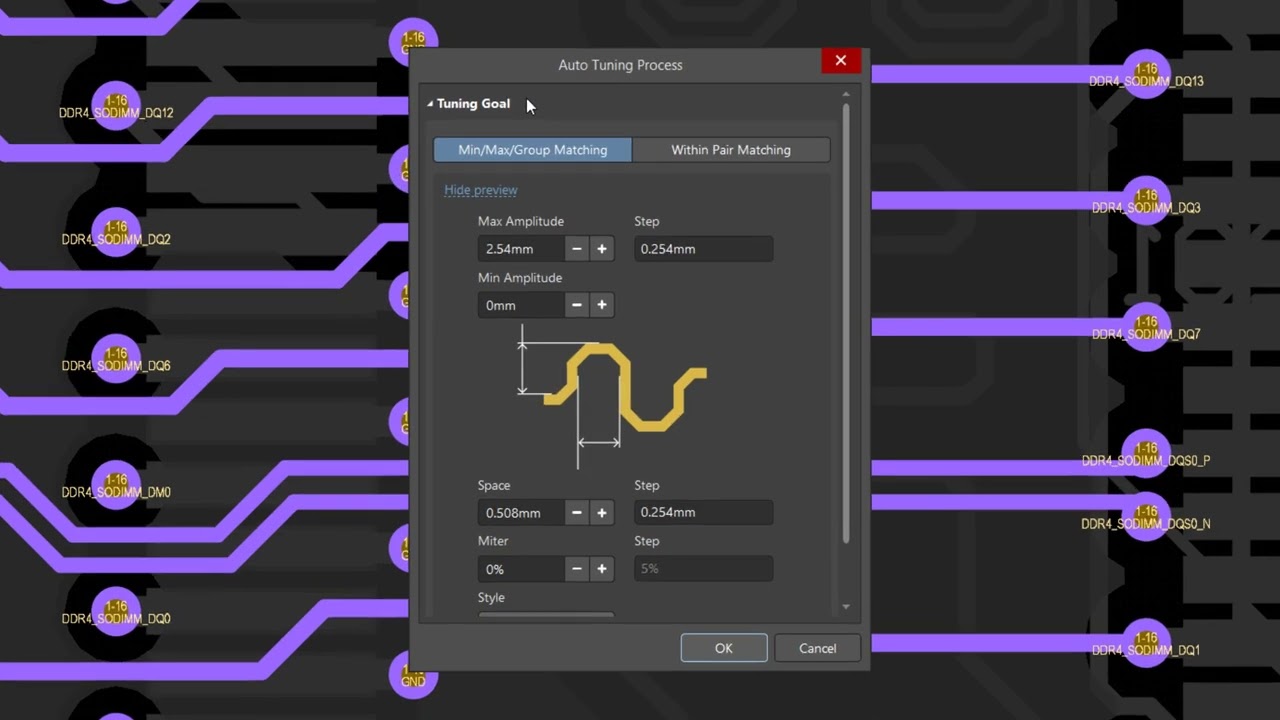
PCB Layout Enhancements
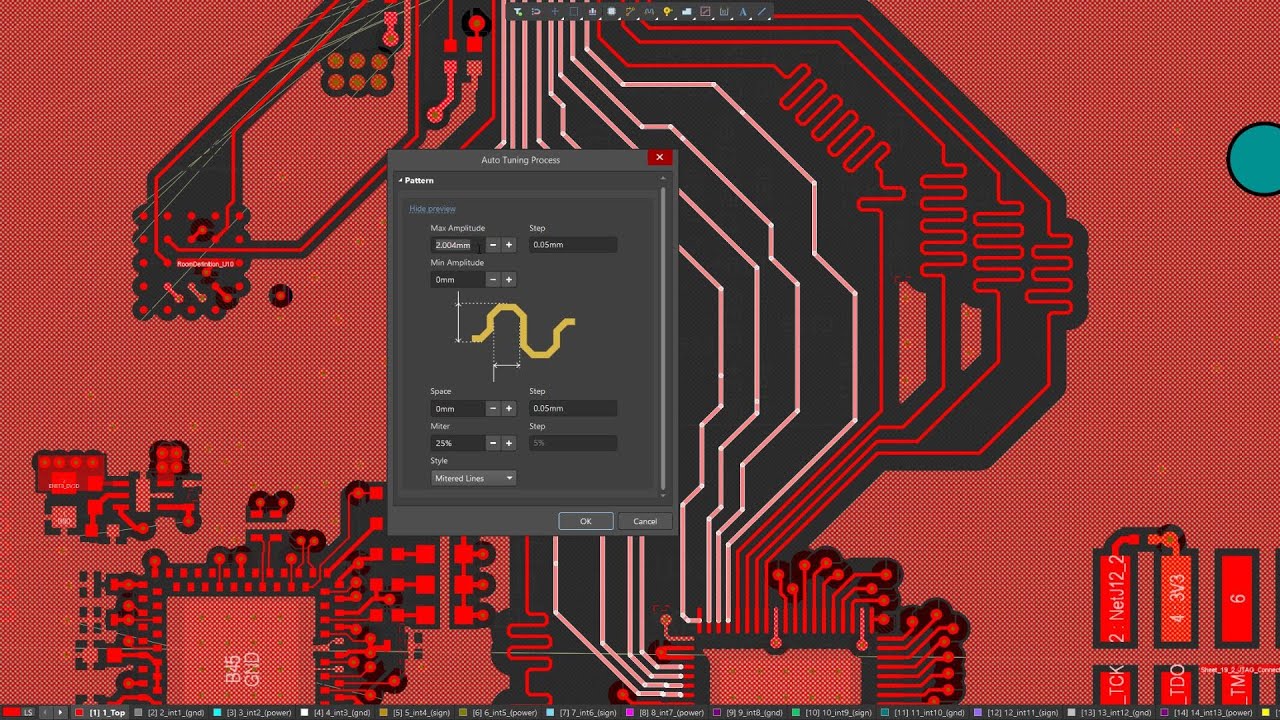
Experience Clearer Terminology in the Auto Tuning Dialog
The Auto Tuning Process dialog has updated terminology, including “Tuning Goal” replacing “Pattern” and revised names for “Accordion” and “Sawtooth” to reflect their specific matching purposes.
Recommended Content:
- To learn more about PCB Layout in Altium Designer, visit the resource page.
- Visit the PCB Layout documentation page.
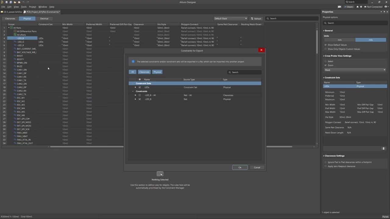
Constraint Manager Enhancements
Export and Import Your Constraints with Unified Commands
The export and import processes for constraints and constraint sets have been streamlined into single commands.
Recommended Content:
- To see an overview about the Constraint Manager, visit the feature page.
- Check out our recent OnTrack Podcast video on the Constraint Manager, Deep Diving Into Altium Designer's New Constraint Manager.
- Visit the Constraint Manager documentation page.
Wire Bonding Improvements
Place Die Pads by Height with Wire Bonding Support
Die pads are now bound, by height, to the 3D body they are placed on instead of the highest 3D body in the die pad location.
Recommended Content:
- To see an overview, visit the feature page.
- Watch the recording of our recent webinar, Unlock New Design Possibilities with Wire Bonding.
Multi-board Design Improvements
Use External Components in Your Multi-board Designs
Multi-board design now has support for placing external peripherals/components that are not part of the regular child PCB board assemblies.
Recommended Content:
- To see an overview visit the Multi-board Design feature page.
- Check out our recent webinar on system design, Unlock Complete System Design with Altium Designer 24.
- Visit the Multi-board Design documentation page.
Harness Design Improvements
Override the Calculated Wire Length in Your Layout Drawing
Harness Layout Wire Length Override allows you to manually adjust the wire length on a Layout Drawing within a harness design.
Recommended Content:
- To see an overview about the Harness Design tool, visit the feature page.
- Check out our recent webinar on Harness Design, Future-Proof your Wire Harnesses with Altium Designer.
- Visit the Harness Design documentation page to learn more.
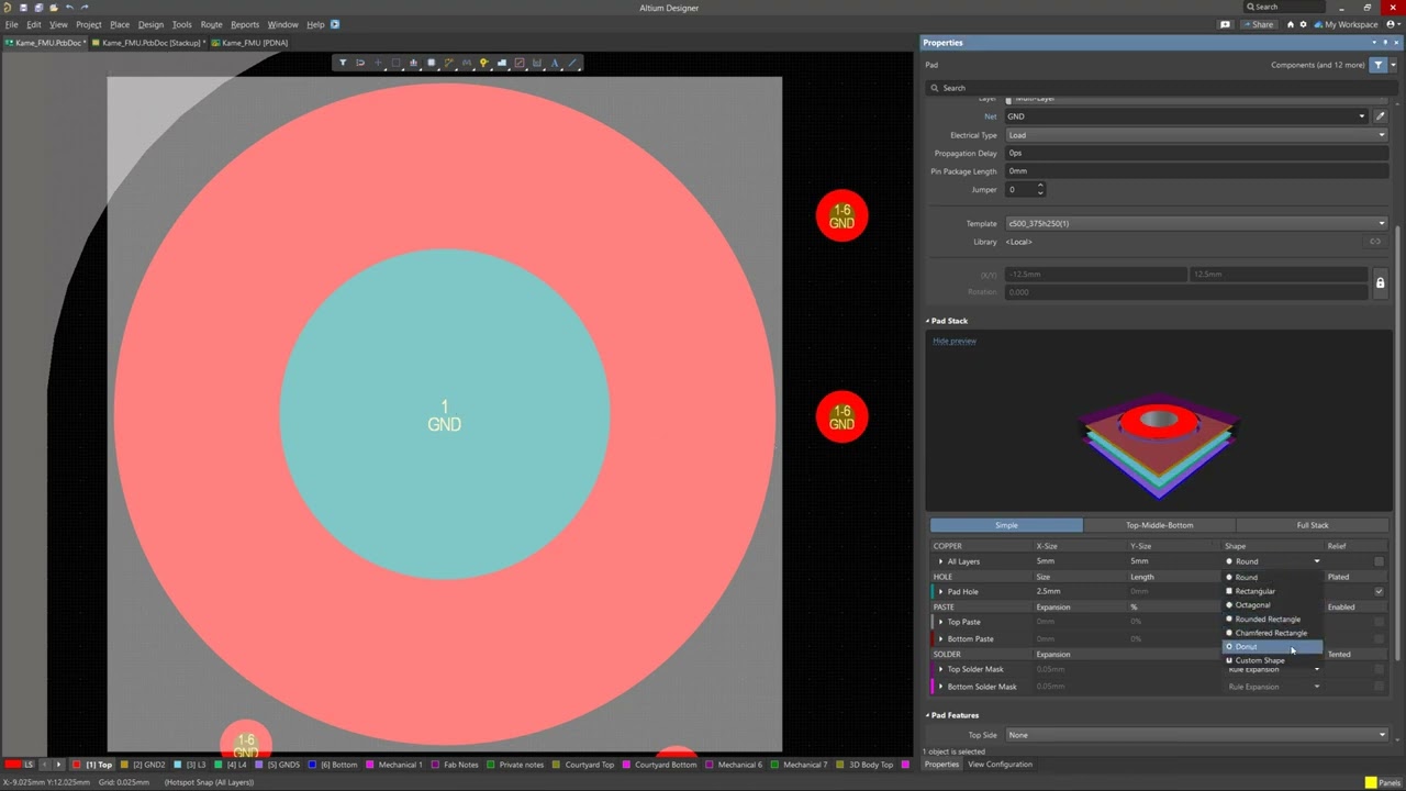
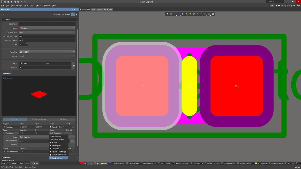
PCB Layout Improvements
Design in Custom Components with Donut Pad Support
You can now create true round donut pad shapes in the properties panel.
Recommended Content:
- To learn more about PCB Layout in Altium Designer, visit the resource page.
- Visit the PCB Layout documentation page.
Data Management Enhancements
Ensure Accurate Variant Parameters for Seamless PLM Integration
Variant-level parameters defined in your project now correctly propagate into the assembly parameters upon release to your connected Workspace.
Altium Designer 24
PCB Improvements
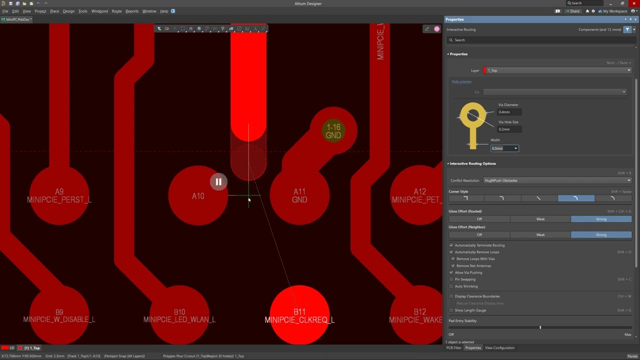
Automatically Narrow Traces in Tight Spaces with Auto-shrinking
The Auto-shrinking feature in the interactive router reduces the width of a trace to ensure it can be routed in tight spaces.
Recommended Content:
- To learn more about PCB Layout in Altium Designer, visit the resource page.
- Visit the PCB Layout documentation page.
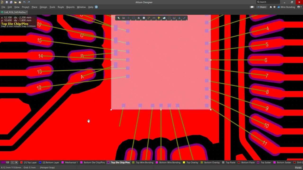
Wire Bonding Enhancements
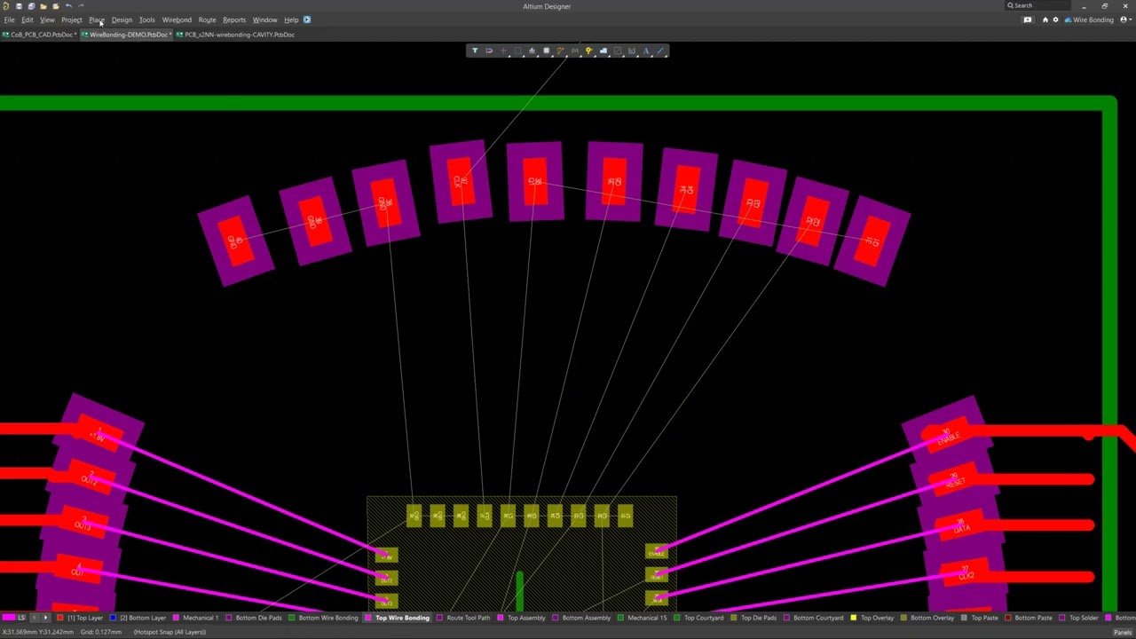
Simplify Chip-on-Board Design with Wire Bonding Support
Wire Bonding Support allows for designing hybrid boards using chip-on-board (CoB) technology, enabling seamless integration of dies directly onto PCBs with bond wires connecting to other components.
Recommended Content:
- To see an overview, visit the feature page.
- Watch the recording of our recent webinar, Unlock New Design Possibilities with Wire Bonding.
Harness and Multi-board Enhancements
Gain Insight with Harness and Multi-board View Only Mode
Harness & Multi-board View Only Mode in allows users with a Standard Subscription or Viewer License to access and explore Harness and Multi-board projects without editing rights.
Recommended Content:
- To see an overview visit the Harness Design and Multi-board Design feature pages.
- Check out our recent webinar on system design, Unlock Complete System Design with Altium Designer 24.
- Visit the Harness Design or Multi-board Design documentation pages.
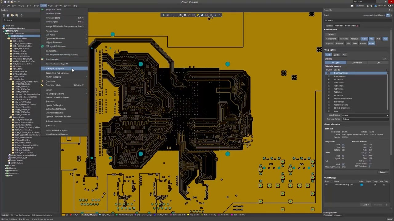
Signal Integrity Enhancements
Ensure Signal Integrity with the SI Analyzer by Keysight
This downloadable software extension allows you to perform signal integrity analysis directly within your design environment in Altium Designer.
Recommended Content:
- To see an overview, visit the product page.
- To see the Signal Integrity Analyzer in action, watch the video tutorials.
- Watch the recording of our webinar, Signal Integrity Made Simple.
Constraint Manager Enhancements
Enable or Disable Rules Directly in the Constraint Manager
Easily manage your PCB design rules with the ability to enable or disable basic rules directly from the All Rules view in the Constraint Manager from the PCB.
Recommended Content:
- To see an overview about the Constraint Manager, visit the feature page.
- Check out our recent OnTrack Podcast video on the Constraint Manager, Deep Diving Into Altium Designer's New Constraint Manager.
- Visit the Constraint Manager documentation page.
Harness Design Improvements
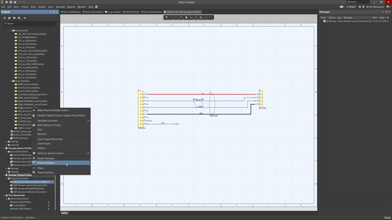
Release Your Harness Design Projects
Simplify your Harness Design release process with Altium Designer's Project Releaser. Automate and manage releases with one-touch ease, reducing errors and saving time, whether working online with Altium 365 or offline.
Recommended Content:
- To see an overview about the Harness Design tool, visit the feature page.
- Check out our recent webinar on Harness Design, Future-Proof your Wire Harnesses with Altium Designer.
- Visit the Harness Design documentation page.
3D-MID Design Improvements
Modify Tracks or Add New Vertices to Your 3D-MID Design
Refine your 3D-MID designs with Altium Designer's new track editing features. You can click and drag to modify tracks or add new vertices, giving you more control and precision in your design process.
Recommended Content:
- To see an overview about the 3D-MID Design Tool, visit the feature page.
- Visit the 3D-MID Design documentation page.
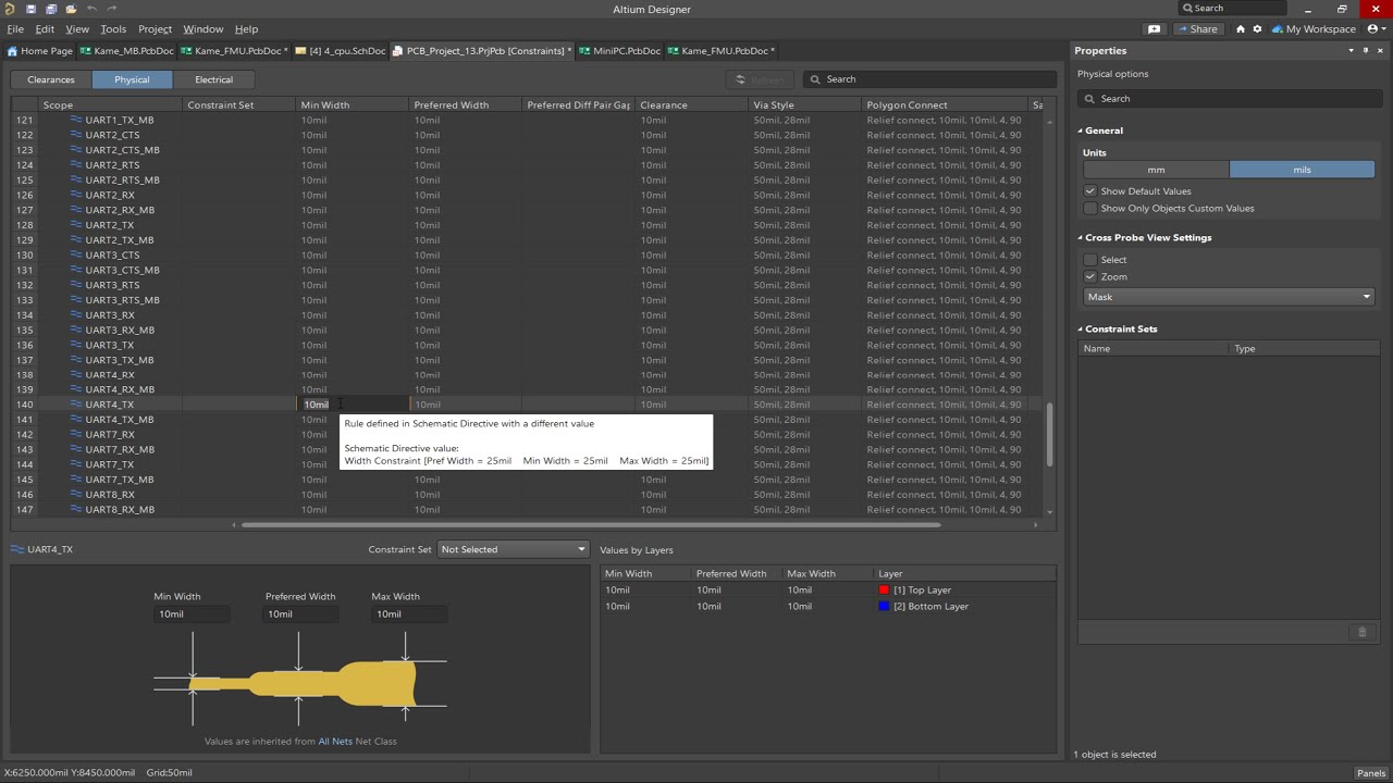
Constraint Manager Improvements
Set Layer-Specific Width Constraints from Your Schematic
When accessing the Constraint Manager from the schematic, it is now possible to choose and configure specific width constraints per layer for any PCB document in the same design project, and independently across layer stacks defined for a chosen board.
Recommended Content:
- To see an overview about the Constraint Manager, visit the feature page.
- Check out our recent OnTrack Podcast video on the Constraint Manager, Deep Diving Into Altium Designer's New Constraint Manager.
- Visit the Constraint Manager documentation page.
Harness Design Improvements
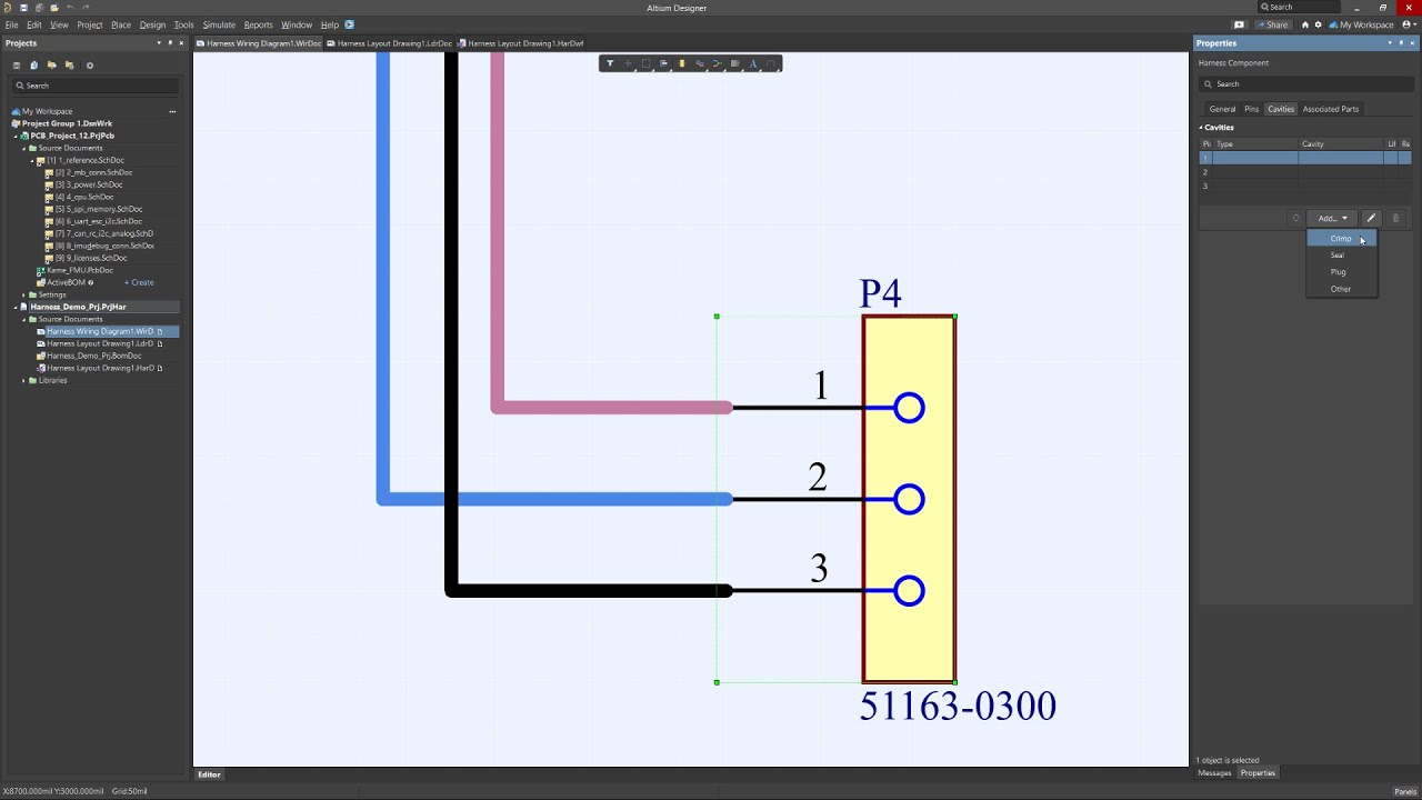
Specify Strip and Pull Off Length for Your Crimps
You now have the ability to specify the 'Strip Length' and 'Pull Off Length' when defining a crimp-type cavity in the Wiring Diagram.
Recommended Content:
- To see an overview about the Harness Design tool, visit the feature page.
- Check out our recent webinar on Harness Design, Future-Proof your Wire Harnesses with Altium Designer.
- Visit the Harness Design documentation page.
3D-MID Enhancements
Select and Drag Multiple Components in 3D-MID Design
3D-MID Design now includes the ability to select and drag multiple components on the substrate. This enhancement allows users to easily reposition multiple components simultaneously on the 3D substrate.
Recommended Content:
- To see an overview about the 3D-MID Design Tool, visit the feature page.
- Visit the 3D-MID Design documentation page.
PCB Improvements
Design Single-Layer PCBs with Integrated Layer Stack Management
The Single Layer PCB Support feature in Altium Designer allows users to create single-layer PCBs, with full integration in the Layer Stack Manager and related outputs.
Recommended Content:
- To learn more about Layer Stack Manager in Altium Designer, visit the documentation page.
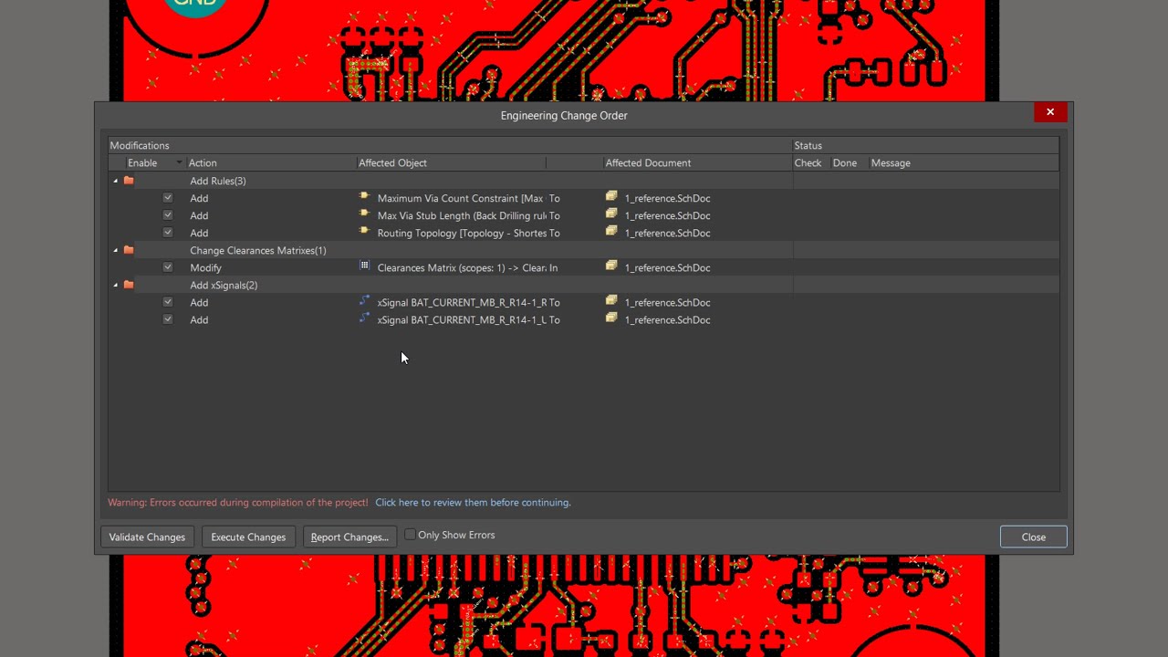
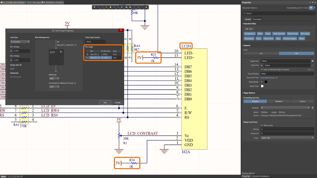
约束管理器增强
在约束管理器中导入指令的值
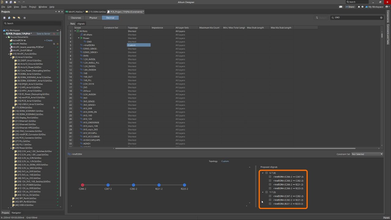
现在,可以通过新的对话框功能在约束管理器中汇总从原理图导入的值,以更加直观的方式将约束可视化。还可以在设计区中以蓝色显示导入的指令,从而与不同符号进行区分,并在属性面板中访问相应规则。支持在约束管理器中直接通过定向ECO传播从PCB创建xNet和xNet类,以简化PCB与原理图之间的同步工作。此外,针对双引脚网络选定Custom拓扑结构后,即可自动将其引脚作为节点添加到拓扑结构编辑区域,以便于选定建议的xSignals。
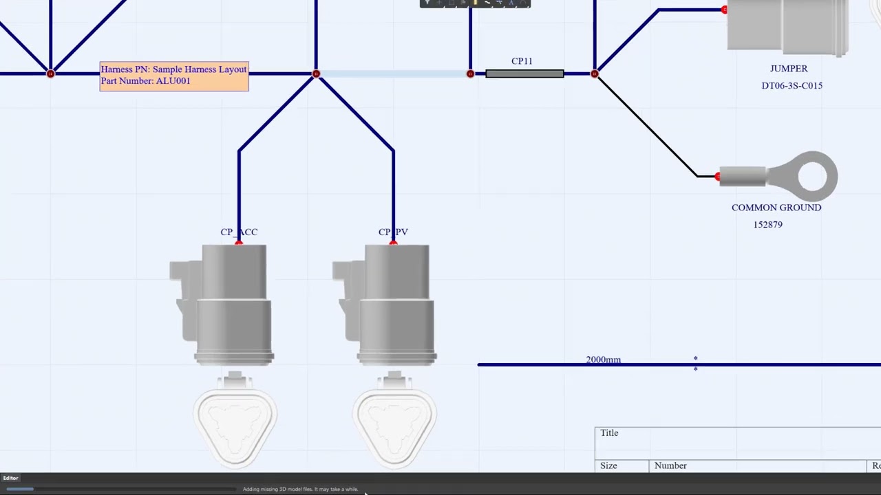
线束设计增强
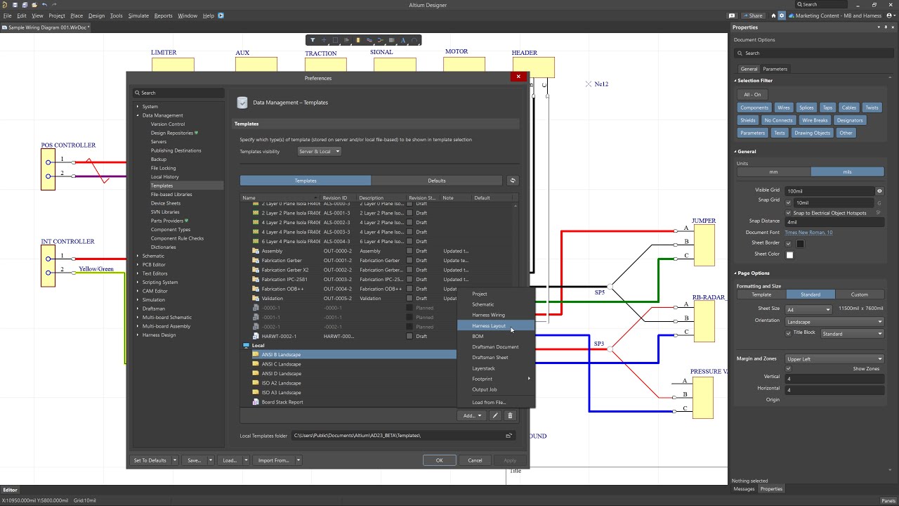
创建线束设计模板
您可以在连接的Altium 365 Workspace中轻松创建、上传、编辑并复用Harness Wiring Diagram和Harness Layout Drawing模板,以简化工作流程。此外,Altium Designer还通过在Wiring Diagram中纳入对象‘Type’字段以及在Layout Drawing中纳入标签和覆盖层,增强了对设计的控制,从而可以精确管理是否将其包含在BOM中。另外,现在可以向屏蔽对象分配一个库ID,以增强其组织性和可访问性。Altium Designer简化了导线颜色定义,可以在Wiring Diagram中使用单个颜色参数来反映二次和三次配色,从而提高了导线的可见性和清晰度。在引入导线对象的‘Include Cut’参数后,您可以控制是否将其包含在Harness Draftsman文档的Wiring List中。
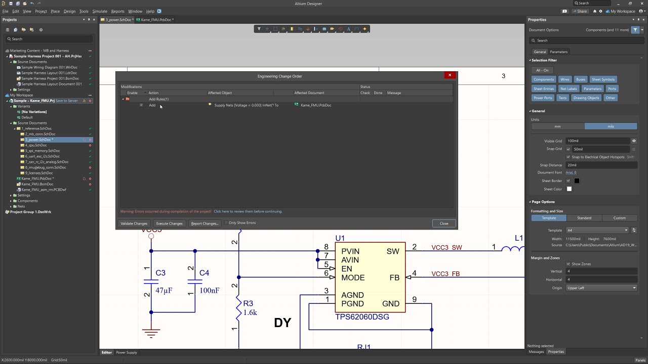
原理图输入改进
自动添加Supply Nets规则
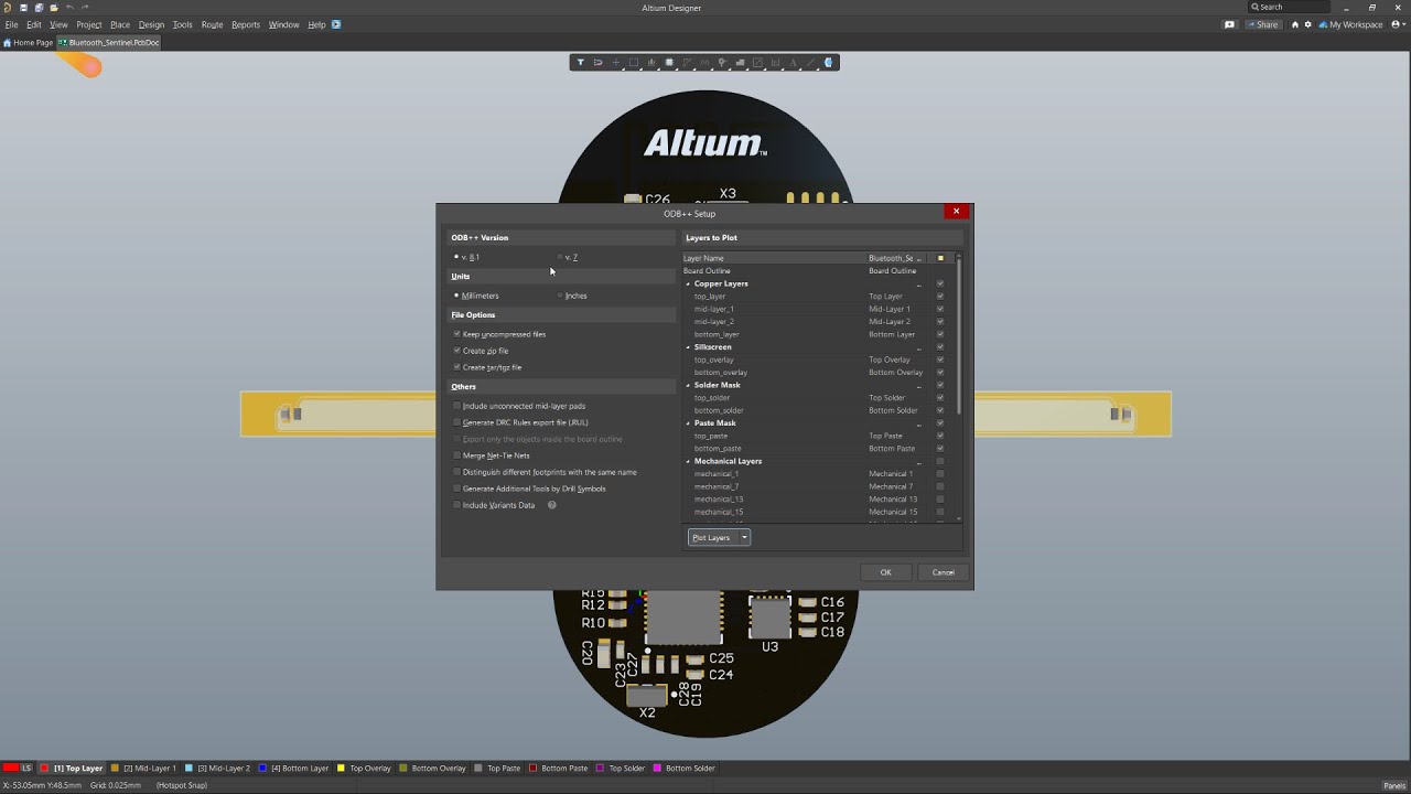
数据生成增强
生成最新v.8.1 ODB++ 格式
您现在可以在单次安装中选择使用最新ODB++ v.8.1或旧版v.7.0格式。您可以集体或单独地为所有已定义变量生成数据,从而简化工作流程。此外,通过整合各种层子类型和支持区域文件,它还简化了柔性/刚柔结合板的制造难度。
PCB 布局增强
防止无意的元件封装镜像
为了便于及早检测到封装镜像,当使用键盘快捷键进行元件或Room翻转以添加安全层时,警告对话框内的选项通常会默认为‘No’。此外,在PCB Health Check Monitor的Components部分,还新添加了一个‘Components with Mirrored Footprints’检查选项,用于检测已放置元件封装与PCB设计区之间的引脚变化情况,以及相关源库中的相应封装。另外,还对‘Update From PCB Libraries’工具进行了功能增强,以检测所有层内位号标识符和三维主体的变化情况,并在Properties选项卡上列出差异。
约束管理器改进
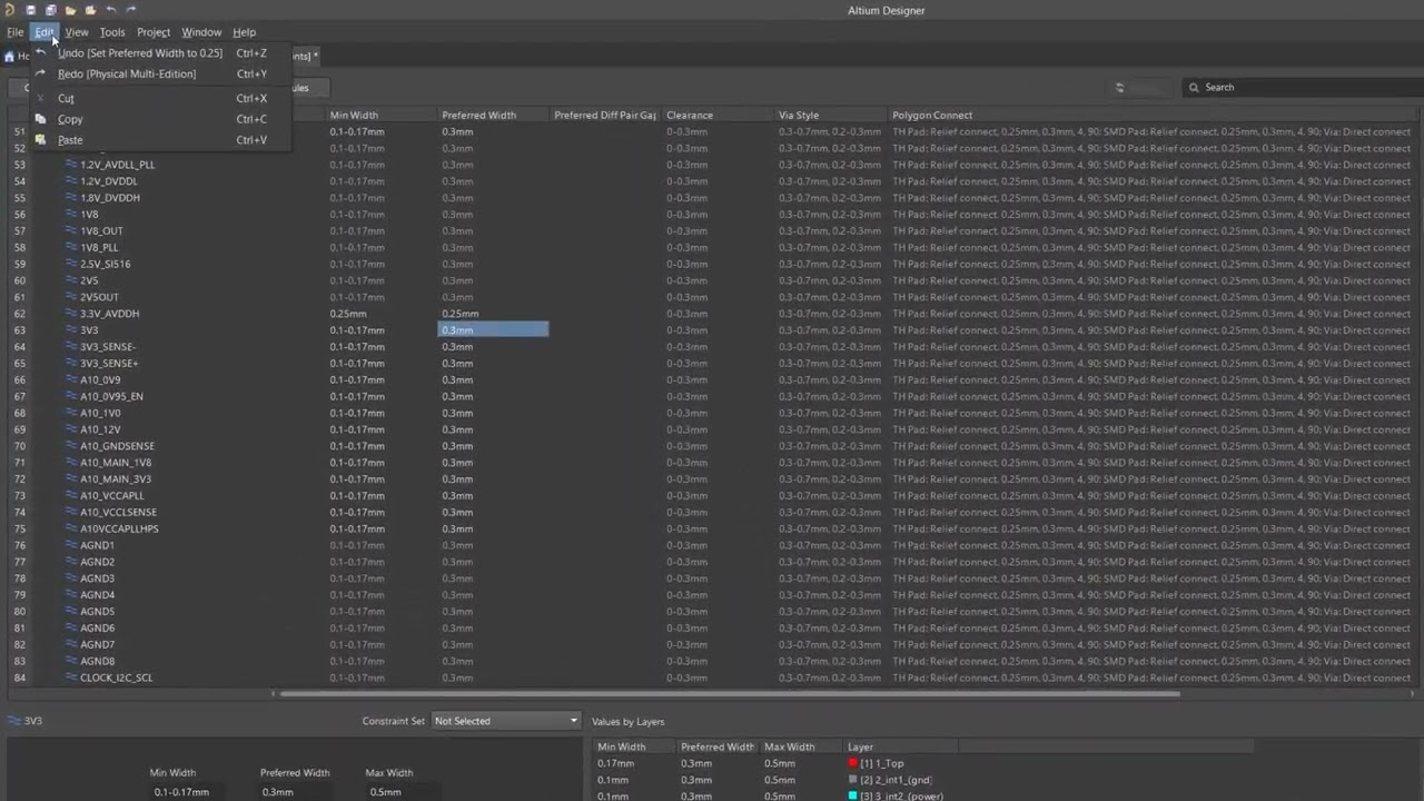
在约束管理器内自动同步宽度值
当您将宽度值输入顶部栅格区域的单个单元格后,该宽度值将自动传播到所有相应的宽度或间距字段。此外,当在原理图中开展工作时,将指示Constraint Manager中定义的约束与源原理图中通过设计指令指定的约束之间的同步状态。
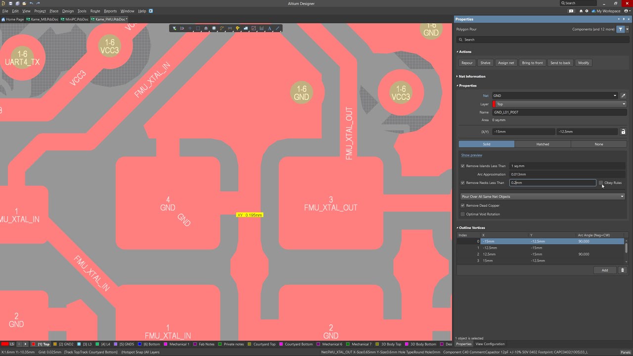
PCB 布局改进
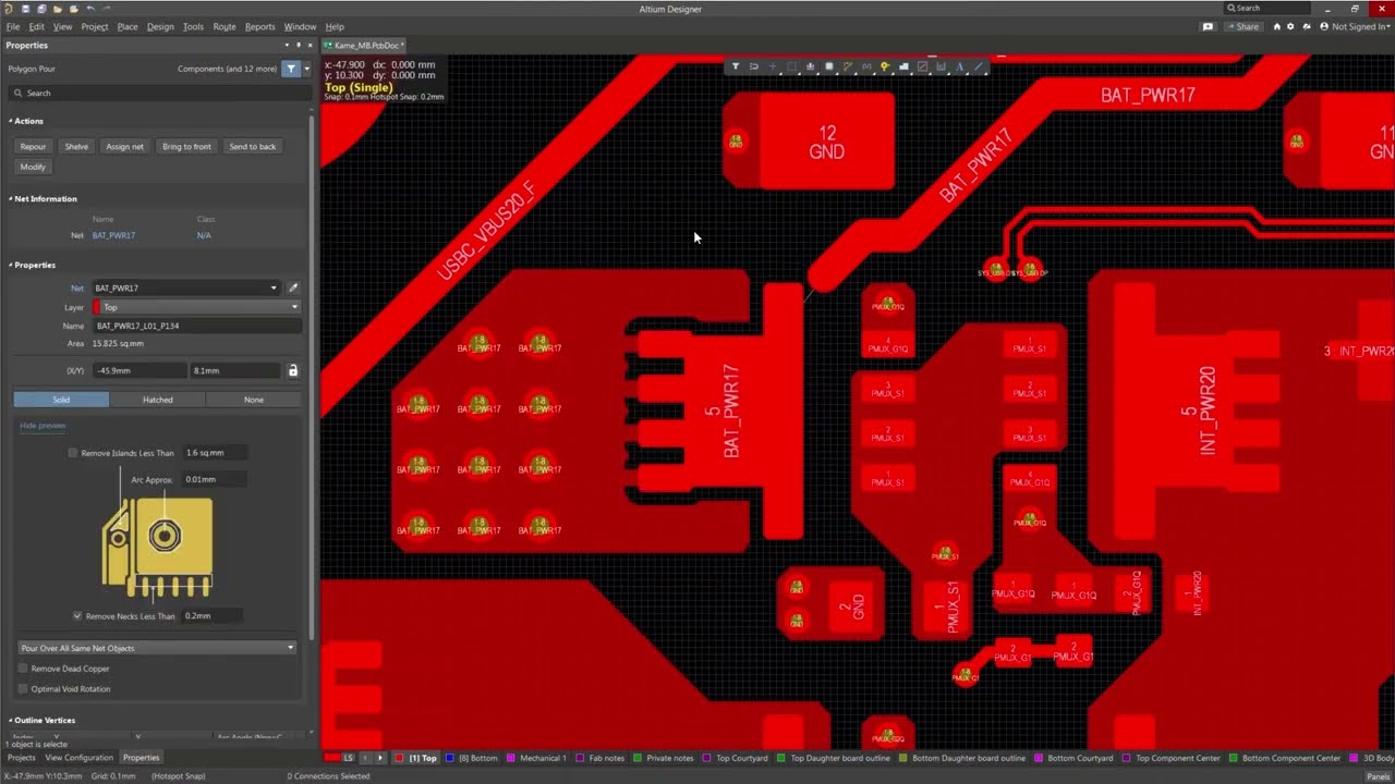
删除小于指定宽度的多边形铺铜颈部
您现在可以使用属性面板中新“Obey Rules”选项,针对已放置的多边形铺铜删除小于指定宽度的颈部。此外,当在“Push Obstacles”模式下移动元件时,Altium Designer 现在会遵守用户为元件选择边界框定义的几何形状。
数据管理改进
查看元件的确切YTEOL值
元件报废年限参数的实际值将会准确显示在SiliconExpert数据的所有实例中,确保了您设计过程中的清晰度和精确度。另外,我们还添加了对SiliconExpert合规性数据表单的引用支持,提升了可访问性和可用性。在将数据库同步到工作区元件时,我们还支持最新的Microsoft Access Database文件格式。
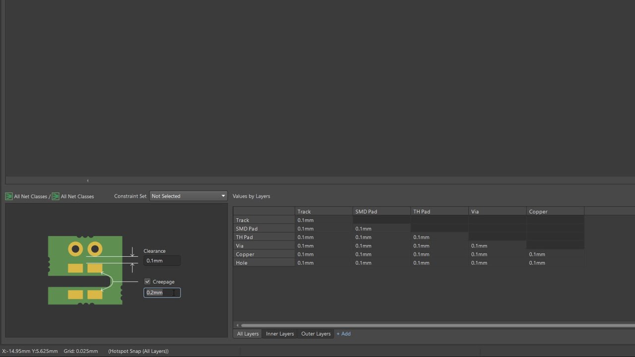
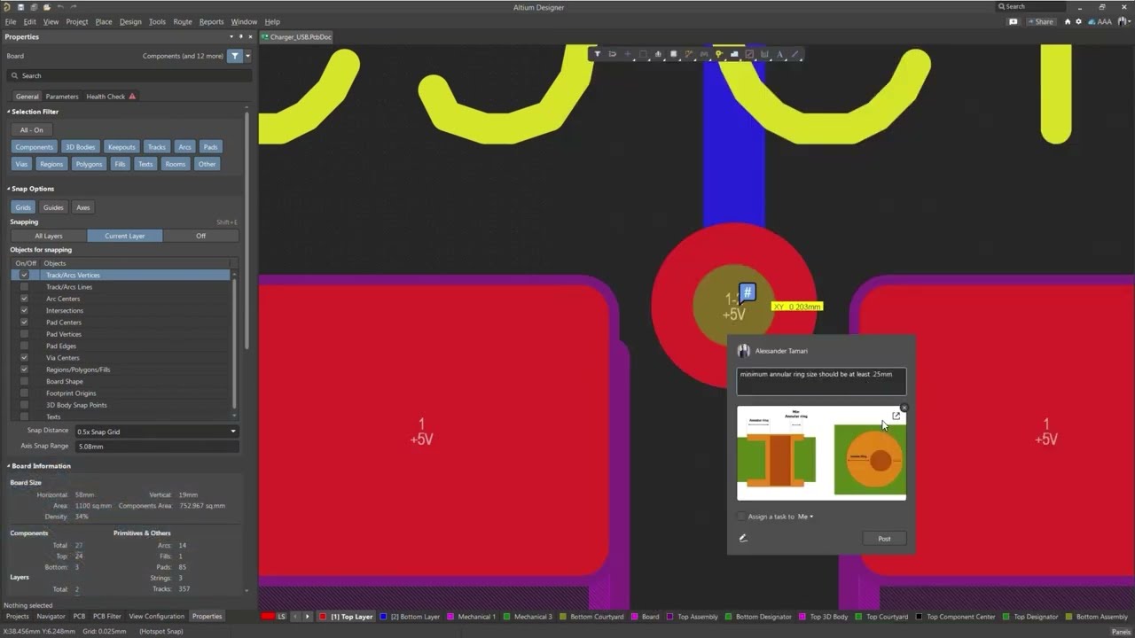
约束管理器改进
使用约束管理器确保准确的电气间距
线束设计改进
为每个线束元件引脚指定详细信息
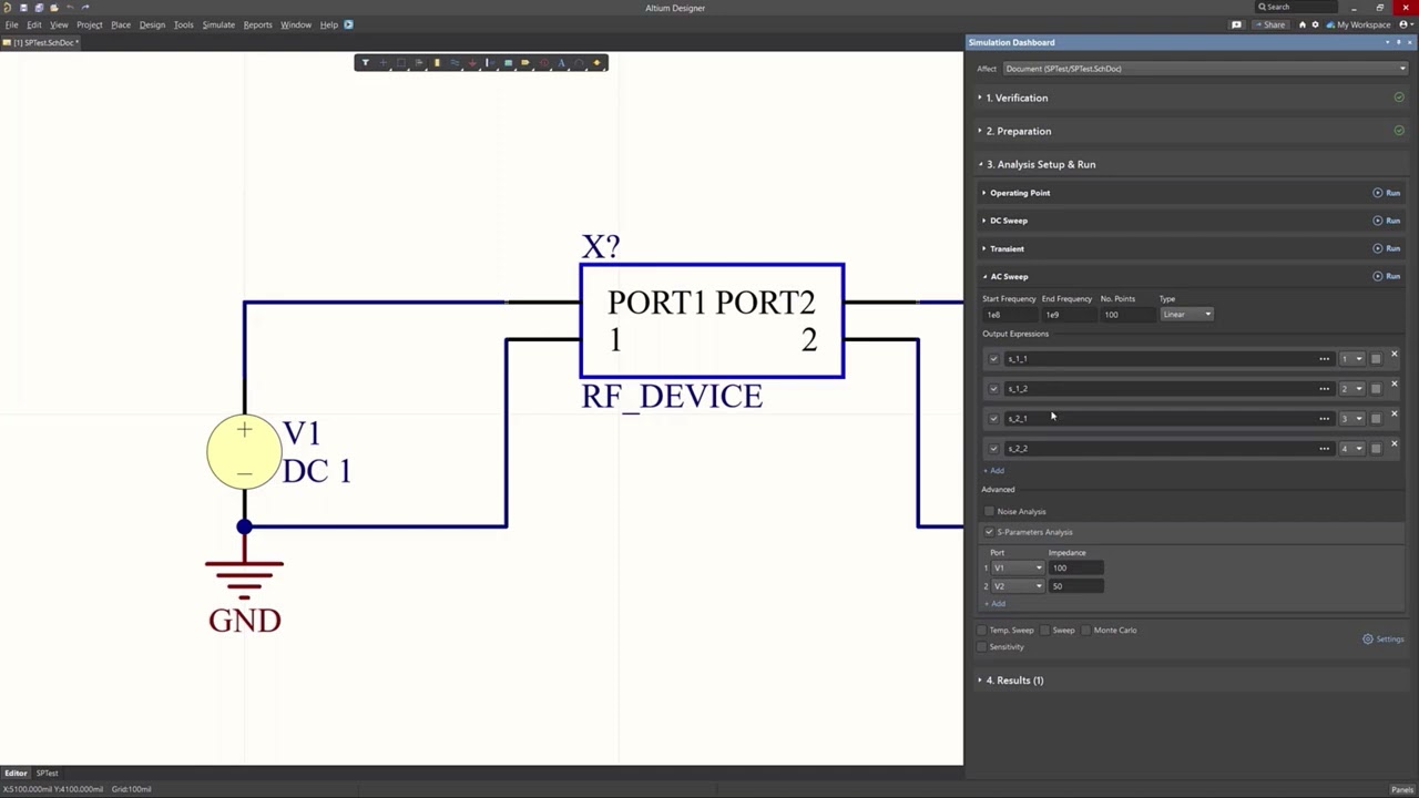
仿真改进
使用S参数进行网络表征
约束管理器改进
在PCB和原理图间传输设计约束
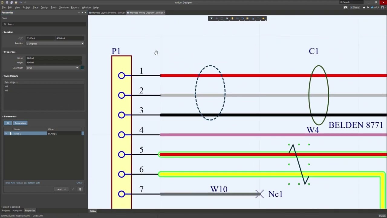
线束设计改进
在线束设计中将导线设置为多色
约束管理器增强
借助约束管理器体验更高控制水平
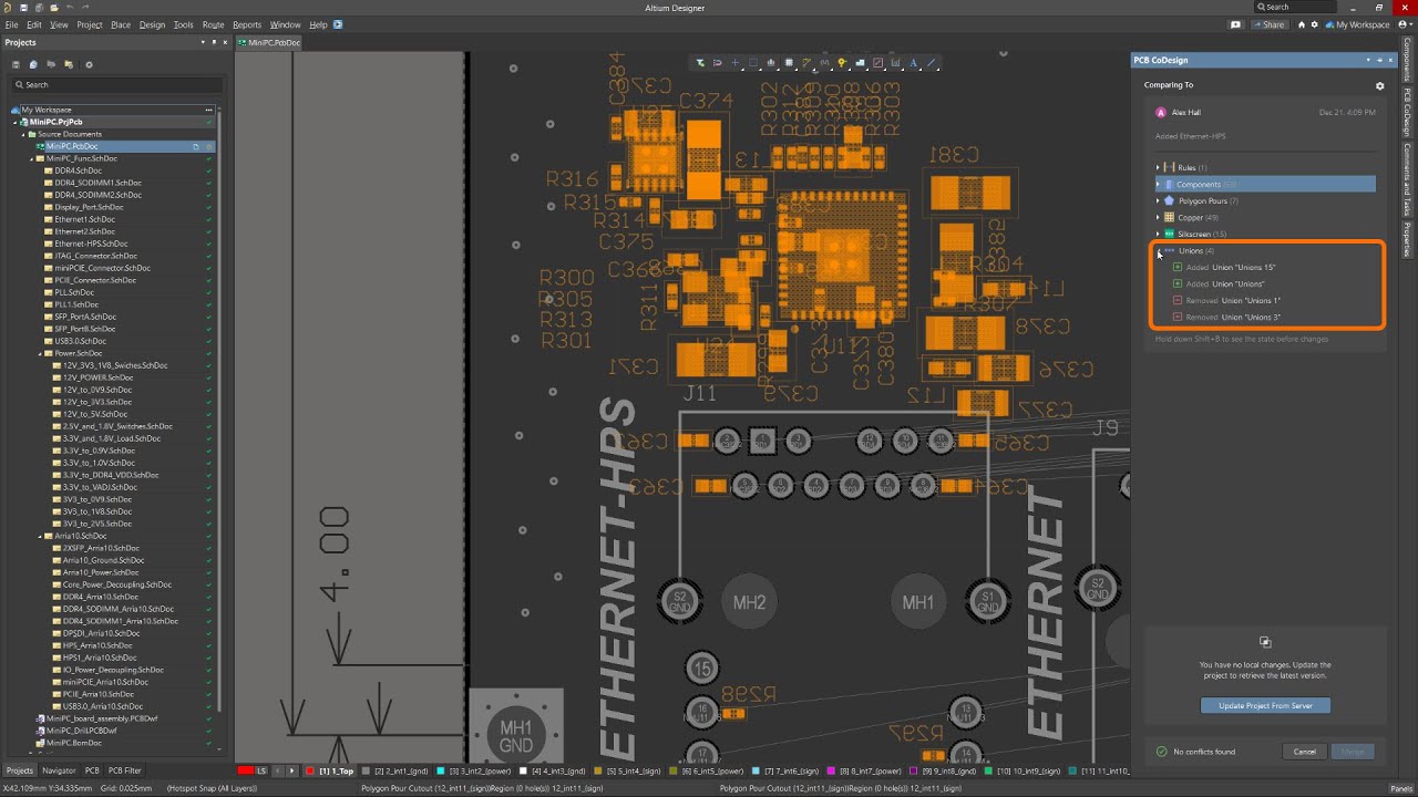
PCB 协同设计改进
借助 PCB 协同设计突出显示特定的已修改类别
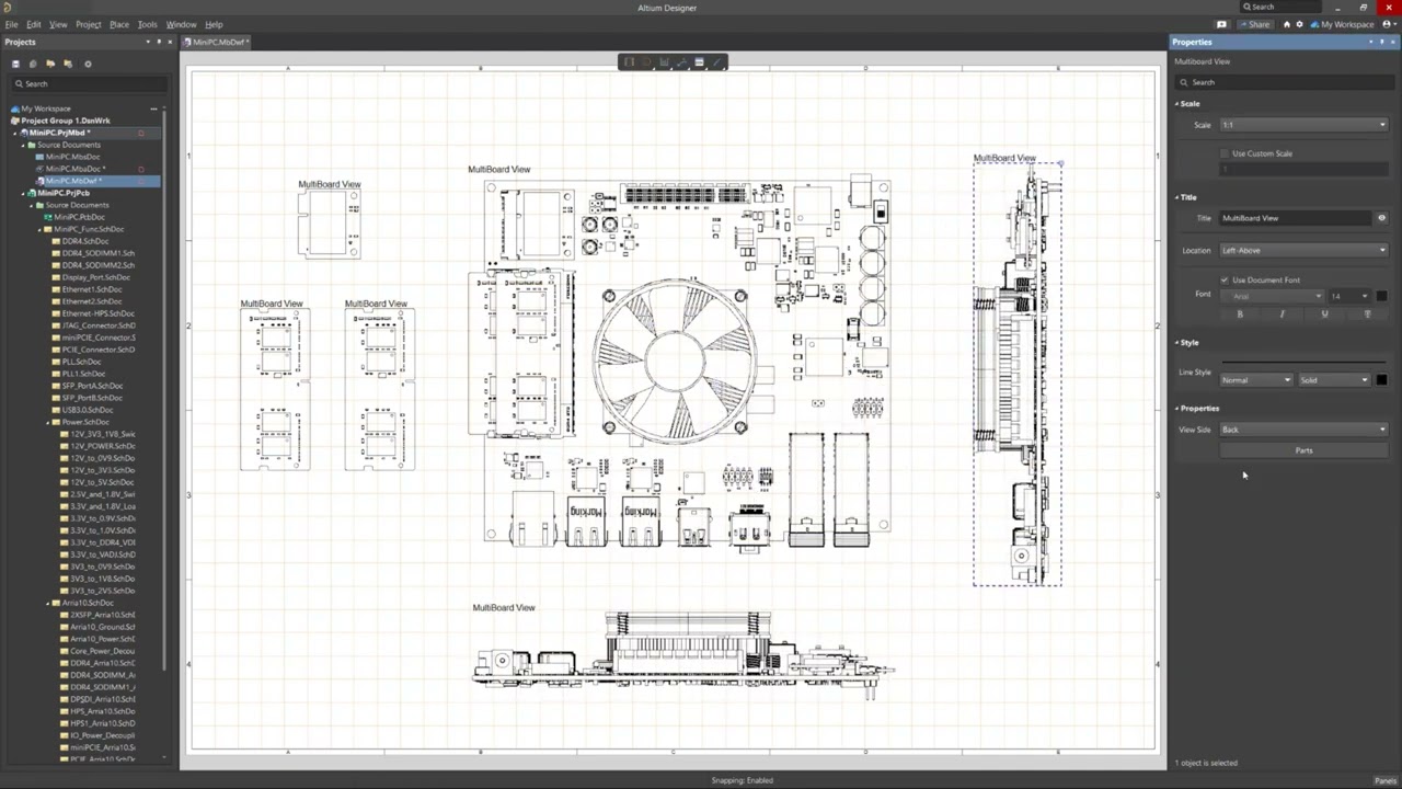
多板改进
为您的多板项目创建清晰的可视化表现形式
使用约束管理器简化复杂的设计规则
使用 PCB 协同设计加速设计进程
使用 3D 机电集成器件工具提升项目水平
Altium Designer 23
使用约束管理器应对任何设计复杂性

PCB改进
以任意角度重塑单端走线

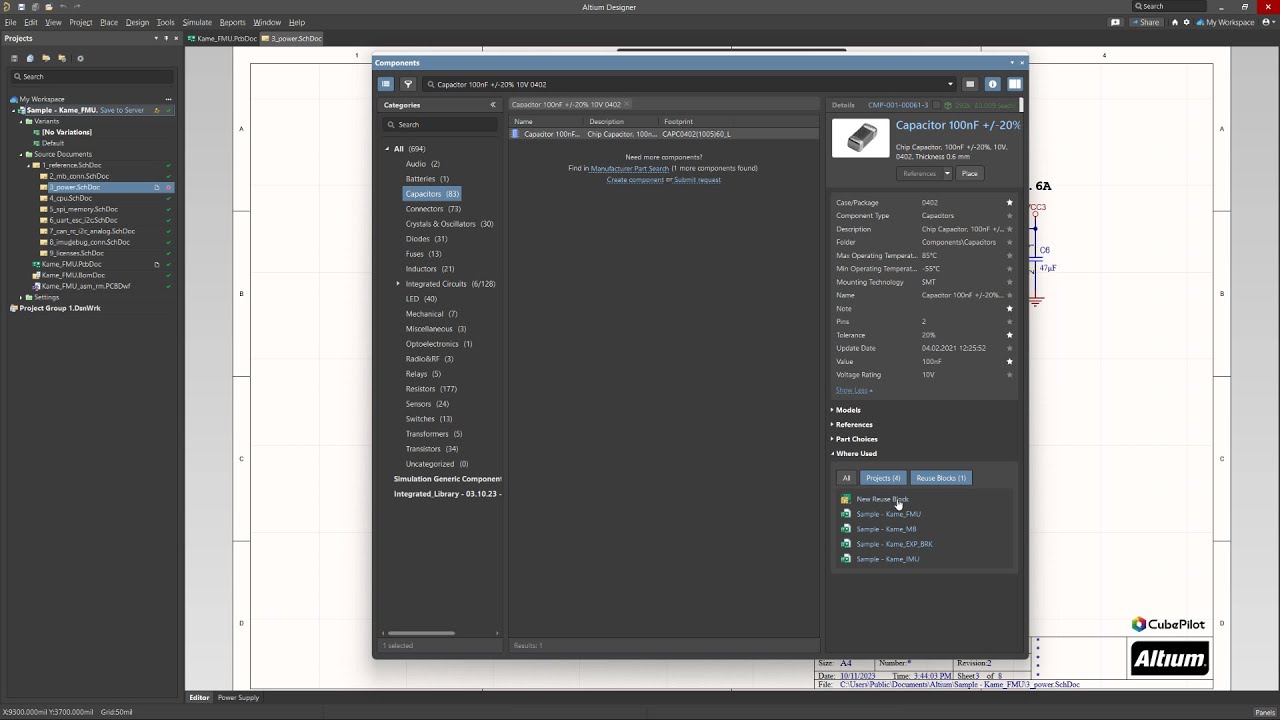
元件管理改进
使用“Where Used”面板跟踪复用块中的元件
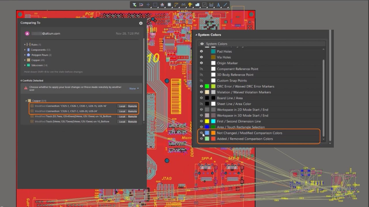
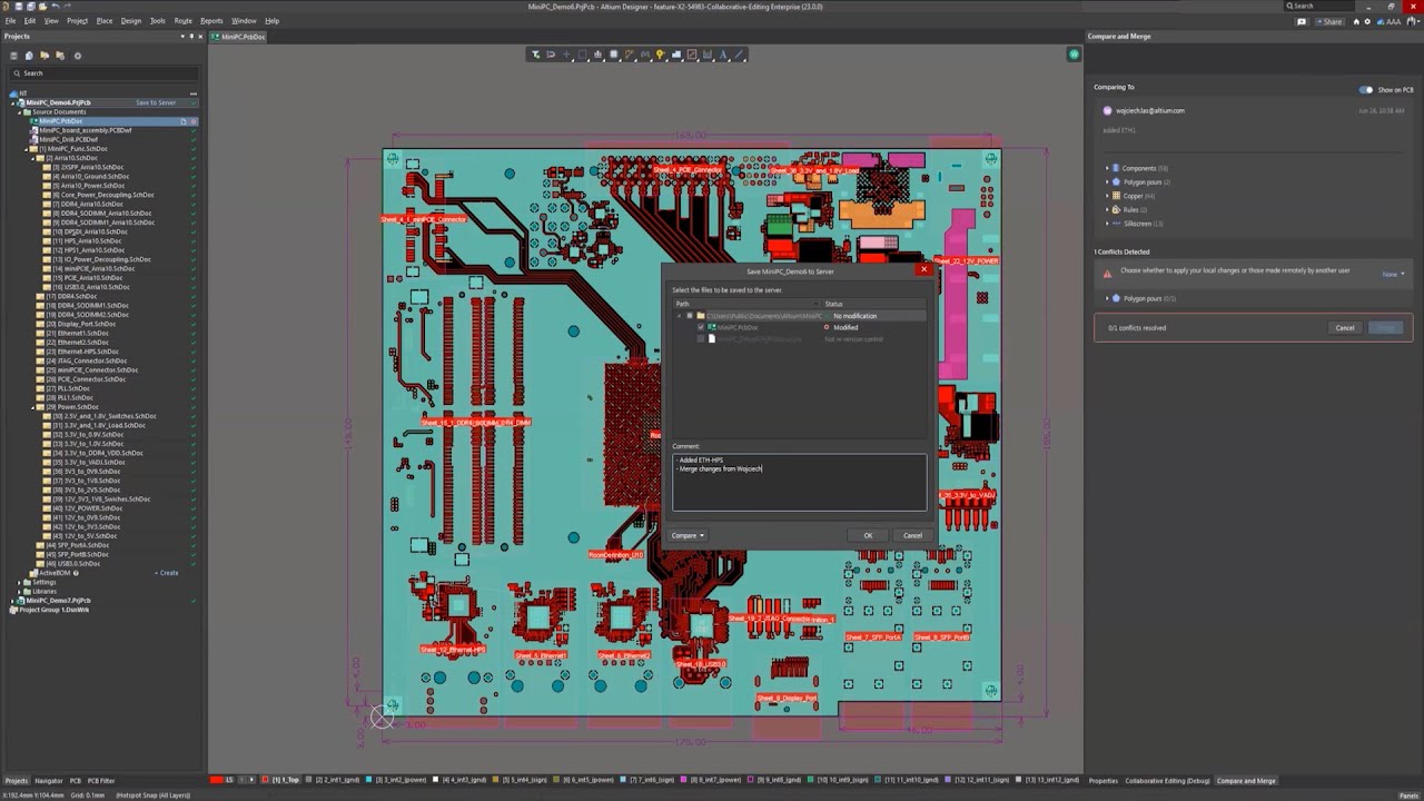
协同改进
通过PCB CoDesign功能实现高效协同设计
对于Pro版和Enterprise版订阅,Altium Designer中的PCB CoDesign功能将确保多名团队成员能够同时处理一个项目,以通过简化开发流程,提高测试和迭代效率,如期完成项目,从而彻底改变了协同设计方式。此项功能包括一种类似于Git的版本控制方法,以确保协同人员能够同时访问同一项目,将更改提交至主分支,并使用Commenting and Tasks功能在电路板上进行工作分配。将会以通知的形式提醒团队成员进行提交,通过Compare and Merge面板显示设计差异,并按颜色编码提供反馈。当发生冲突时,例如多名设计人员重复更改,您可以根据需要自行选择保留本地更改,或者接受最新提交的远程更改,从而确保顺利开展协同设计工作。
导入器增强功能
无缝导入OrCAD和Allegro设计文件
在将OrCAD和Allegro设计文件导入Altium Designer时,进行了关键性的改进和修复。这包括对自定义端口连接器的支持、准确的标题块参数处理、元件填充颜色保留以及精确的设计文件导入,从而确保您的设计过程无缝进行。

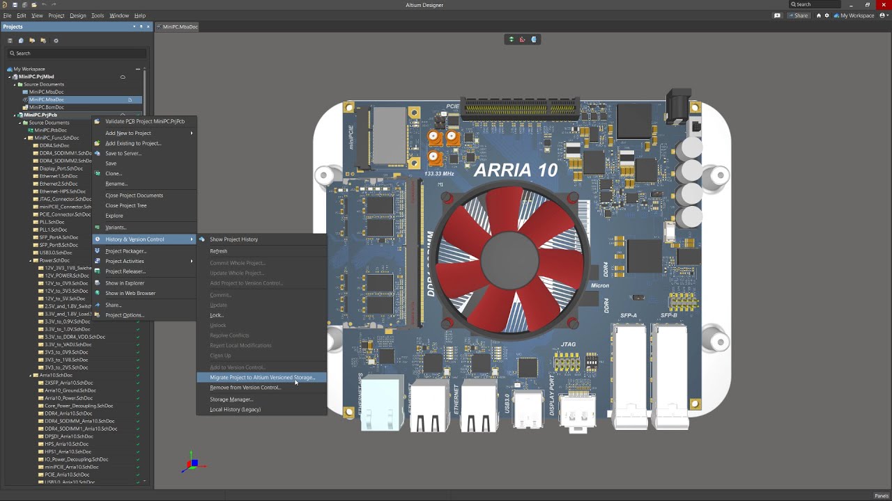
SVN 到 Git 迁移
将设计项目从 SVN 迁移到 Git
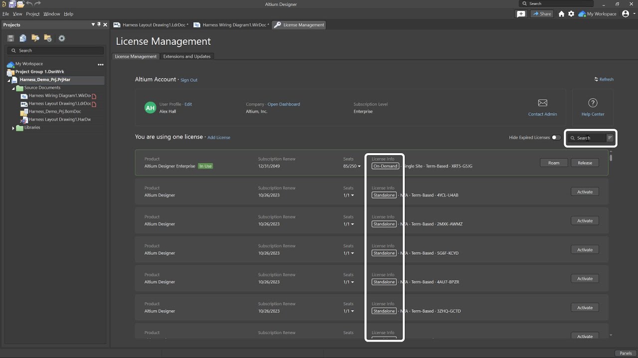
许可证管理改进
通过增强导航和标签功能,优化许可证管理
PCB 协同设计改进
添加了 Room 方向保持功能
PCB 协同设计改进
添加了可用于制造和装配说明的新特殊字符串
PCB设计改进
轻松管理设计中每个元件的零部件选择
电路仿真改进
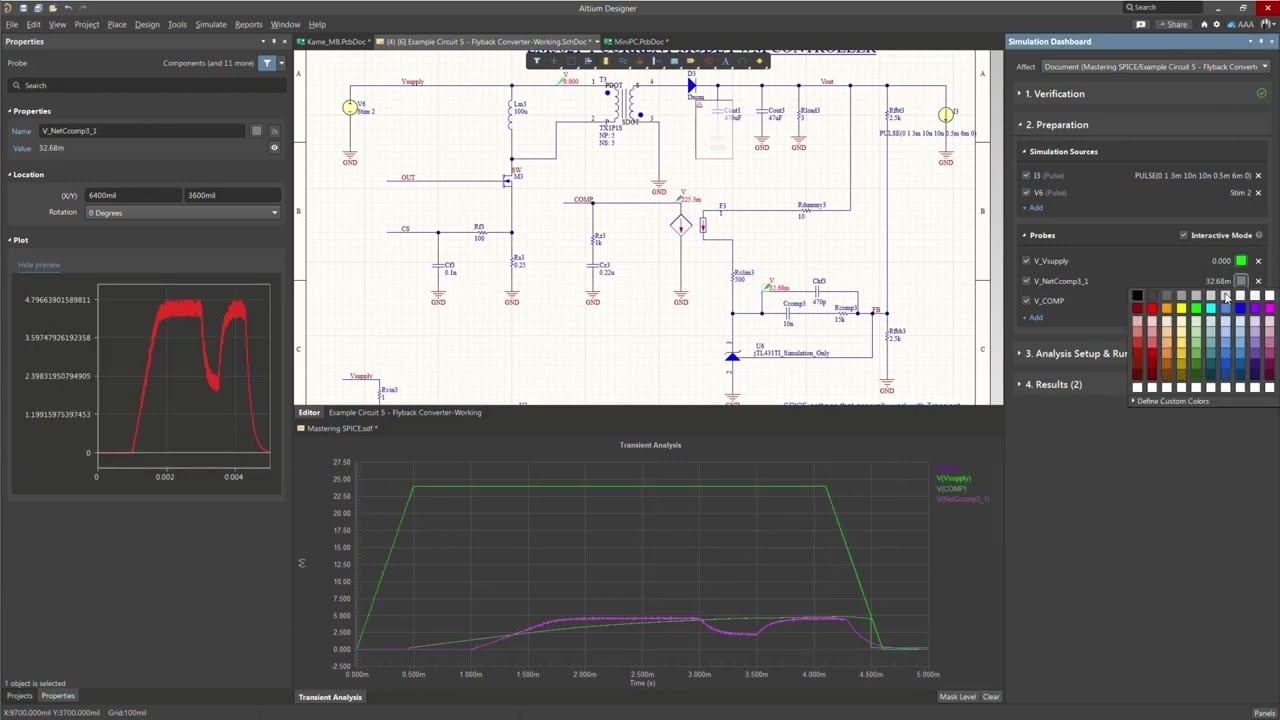
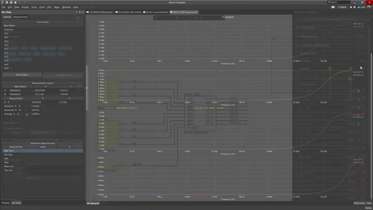
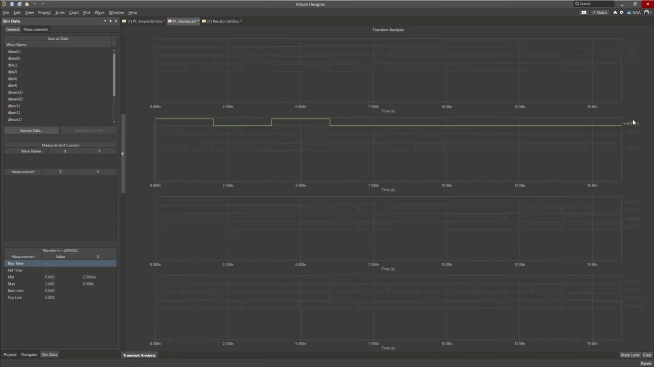
使用新仿真数据查看器精确测量结果
PCB 协同设计改进
精确定位丝印,为封装创建和 PCB 制造做准备
电路仿真改进
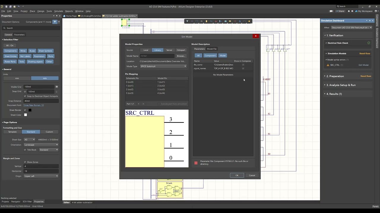
在仿真过程中使用 FSTIM 激励模型
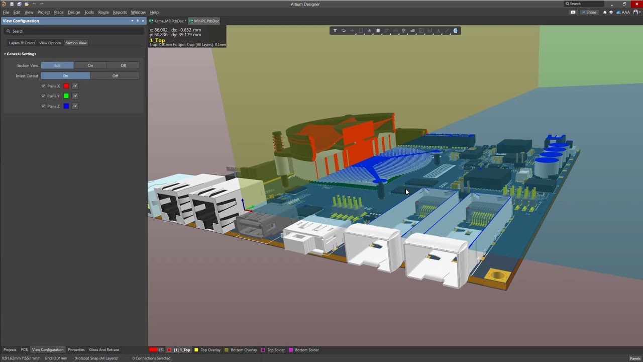
使用 PCB 剖面图功能查看隐藏元件
PCB 的剖面图功能为您的设计提供了前所未有的精确洞察,揭示了 PCB 布局和结构中通常不可见的细节。当处理密集和复杂的 PCB 时,剖面视图可以显示 PCB 中的细节。通过控制平面的放置和颜色,您可以轻松查看所有元件,甚至是隐藏在较大元件或机械零部件下的较小 SMD 元器件。
定制热风焊盘
使用实时仿真探测来测试您的电路
电路仿真支持受控源和可变无源器件在交流分析中的输出值
我们添加了对电压和电流受控源、函数信号源和可变无源器件的支持,以在进行交流分析时对电压、功率和电流输出变量进行分析。此功能非常适合音频项目、通信设计等设计类型。此外,我们还添加了对多位ADC和ROM PSPICE数字模型基元及其时序模型的支持。
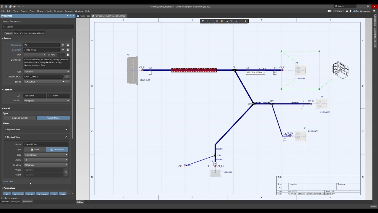
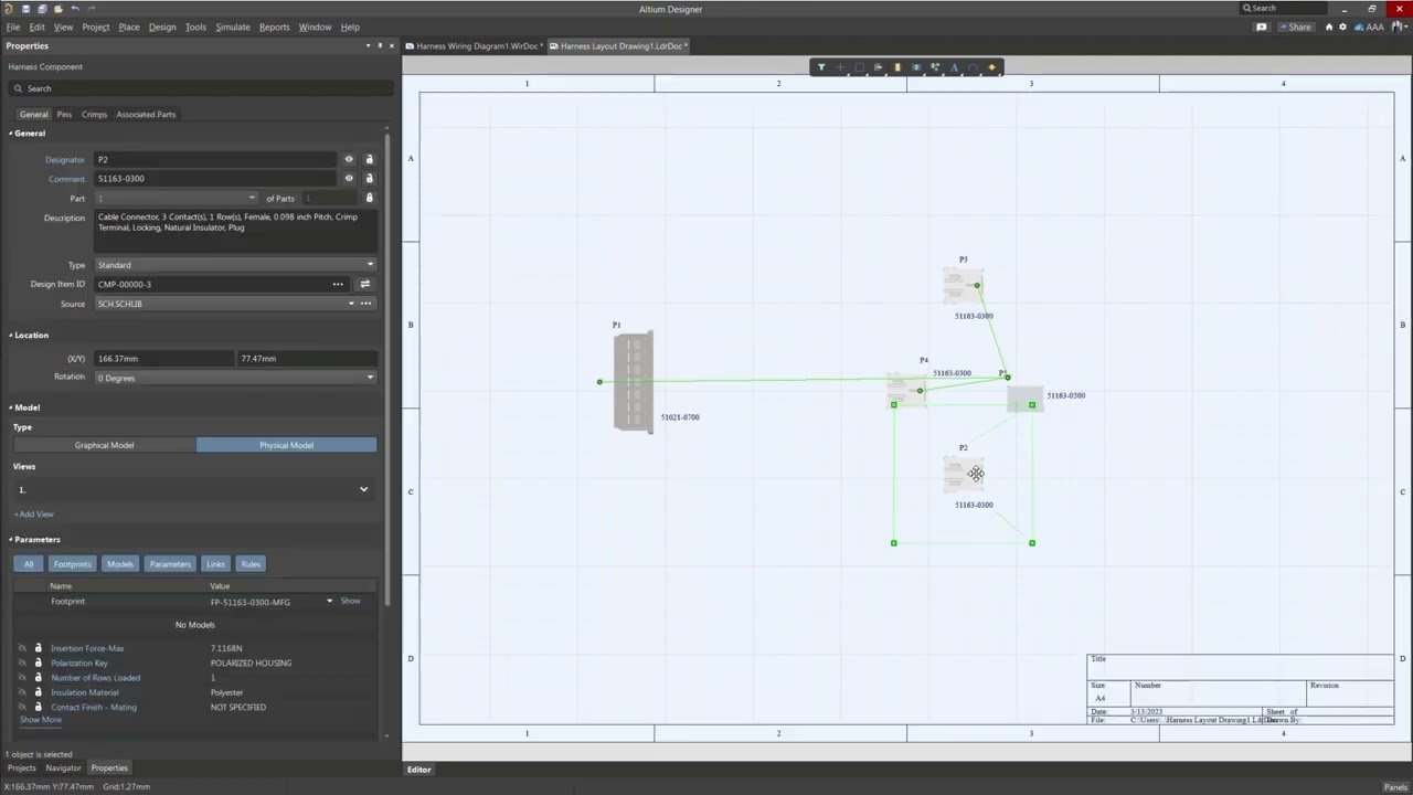
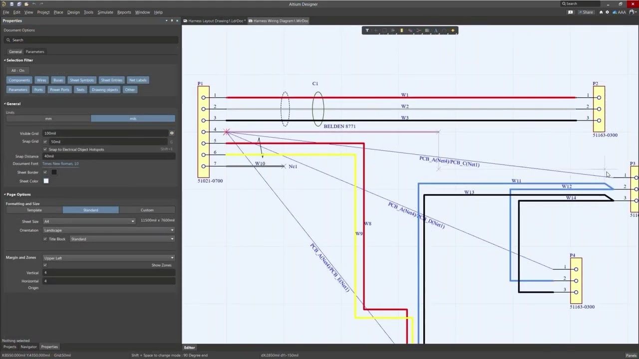
线束接线图对象的实时跟踪和固定纵横比
进行实时跟踪时,操作将主动跟随光标,直接向您展示通往最终导线目的地的路径。从而确保您能够在接线图中更加有效地追踪数据。接线图对象此时将与文档捕捉栅格同步,以将接线图统一性提升至一个新的水平。
线束设计新功能:3D 线框视图和向连接点添加模型
PCB 改进
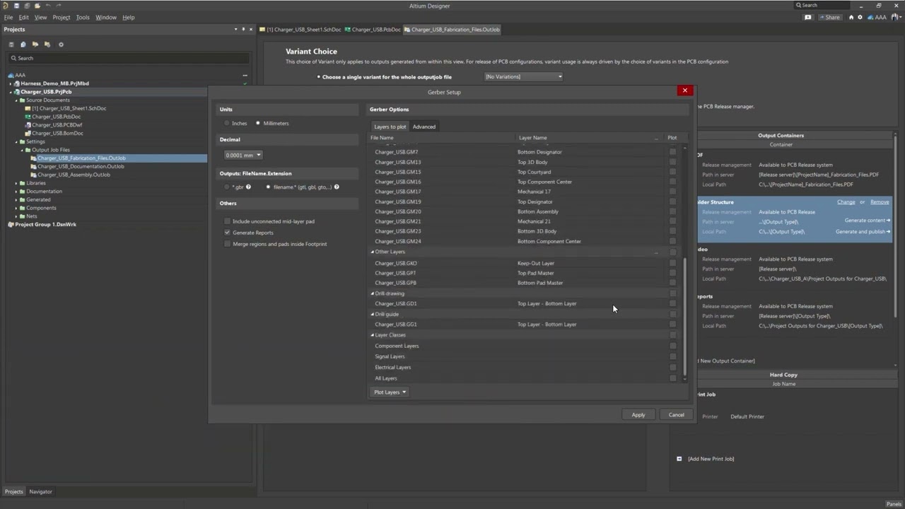
Gerber Setup 层类支持
电路仿真改进
添加了对 PSpice 数字模型的支持
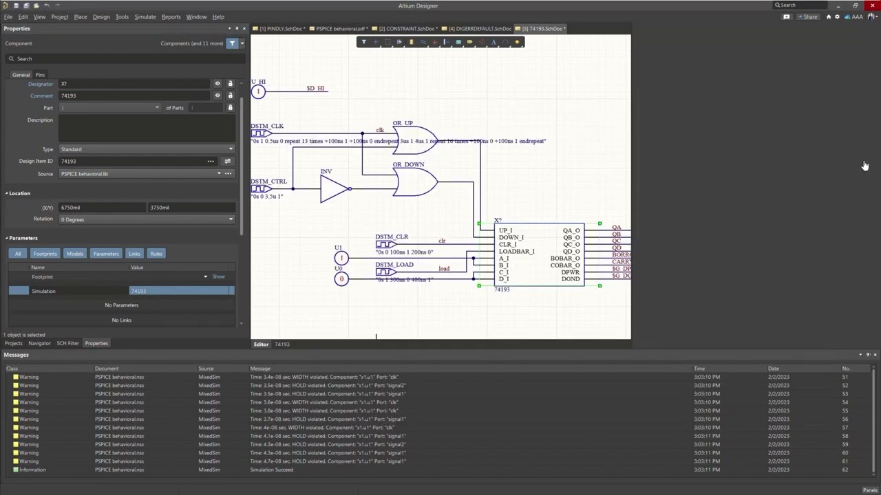
此版本的 Altium Designer 支持更多 PSpice 数字模型基元。我们添加了对 PINDLY 和 CONSTRAINT PSpice 数字行为模型基元的支持,以及对 DIGERRDEFAULT 选项的支持。
线束设计改进
线束设计改进
数据管理改进
协作和报告更新
线束设计改进
其他线束设计能力
PCB改进
用于 Gerber 和视图配置的全新 PCB 功能
这个新的 PCB 功能允许您从视图配置面板加载存储的视图配置文件。此外,在使用新的统一 Gerber/Gerber X2 对话框时,现在还可以更改 Gerber Board Profile 图层的名称。

Altium Designer 22
PCB 改进
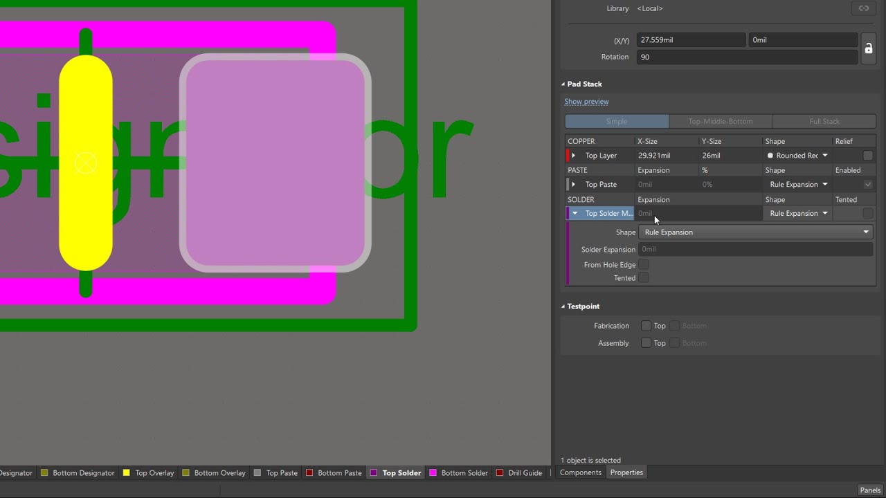
具有圆角/倒角的自定义焊盘形状
只需几次点击,即可按照您的需求塑造焊盘形状。您现在可以通过扩展的多样性焊盘形状,针对具有Rounded Rectangle或新Chamfered Rectangle形状的选定焊盘转角,进行倒角自定义。

PCB 改进
Gerber设置界面功能增强

SPICE仿真改进
其他数字模型和变量支持

数据管理改进
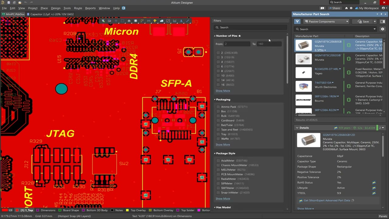
制造商部件搜索UI改进
长期以来,Manufacturer Part Search面板一直是众多用户的元件源。本次发布对其进行了改进,以确保可在其库中更加轻松地使用元件。因此,您可以将更多时间花在开发上而不是流程上!


 沪公网安备 31010502006411号