 Altium Designer 文档
Retired Documentation No Longer Applicable to a Later Version of Altium Designer
Retired Documentation - Panels
Altium Designer 文档
Retired Documentation No Longer Applicable to a Later Version of Altium Designer
Retired Documentation - Panels
PCB面板 - 网络模式
This document is no longer available beyond version 21. Information can now be found here: Browsing Nets for version 24

The Nets mode of the PCB panel
Summary
The PCB panel allows you to browse the current PCB design using a range of filter modes to determine which object types or design elements are listed, highlighted or selected. The panel also has editing modes for specific object types or design elements that provide dedicated controls for editing procedures. Note that you can access the properties for any element listed in the panel.
In Nets mode, the two main list regions of the panel will change to reflect an object hierarchy in order from the top:
- Net Classes, as defined by the board.
- Individual member Nets within a class.
- Individual items (Primitives) within a Net (pads, vias, tracks, and fills).
Panel Access
When the PCB Editor is active, click the Panels button at the bottom-right corner of the workspace then select PCB from the context menu. Alternatively, you can access the panel through the View » Panels » PCB command.
Once the PCB panel has been opened, select the Nets option from the drop-down menu at the top of the PCB panel to enter Nets mode.
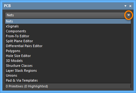
Browsing Nets
Net Classes
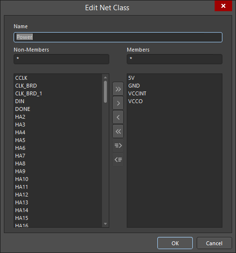
In the top region of the panel (Net Classes), right-click on a net or net item entry then choose Properties from the subsequent menu (or double-click on the entry directly) to access the Edit Net Class dialog in which you can view or edit the net membership of the class, rename it, or add additional classes.
Nets
The middle region of the panel displays nets from the Net Class(es) selected in the region above.

The following information is listed with each Net by default:
-
 - this feature has two functions:
- Color background - the color assigned to the net. This color is always applied to the net's connection lines. It can also be applied to that net's routing using the net color display override feature. Double-click to edit the color for this net, or right-click to edit the color for all currently selected nets.
- checkbox - check this to apply the color to the routing (enable the net color display override feature) for this net. Right-click to enable (or disable) the display override feature for all currently selected nets. Press F5 to enable/disable net color display override in the workspace.
► See Net Color Override - Displaying the Net Color on Routed Nets to learn more.
- Name - name of the net.
- Node Count - the total number of pads in this net.
- Routed Length - the sum of the lengths of the placed track and arc segments that form the routing, plus the vertical distance traversed through vias (see note below). The routed length calculator does not attempt to resolve overlapping track segments or routing wiggles inside pads.
- Signal Length - accurate calculation of the total node-to-node distance. Placed objects are analyzed to: resolve stacked or overlapping objects and wandering paths within pads; and via lengths are included. If the net is not completely routed the Manhattan (X + Y) length of the connection line is also included.
The following notes apply to Signal Length calculations:
- Resolves overlaps and wiggles inside pads.
- Handles routing paths created with objects other than tracks and arcs (e.g., a region or a fill).
- Includes vertical distances through vias (see note below).
- Includes the Total Pin/Package Length for this net.
- Includes the Un-Routed (Manhattan) Length for this net.
- Failure to comply with applicable Length/Matched Length design rules is flagged by the signal length being displayed on a colored background: signal lengths that are too short in yellow, signal lengths that are too long in red.
► See Length Tuning to learn more about how the Length and Matched Length design rules are applied. - A signal is a point-to-point entity; for this reason, only nets with two nodes will show a Signal Length in the Nets mode of the panel (nets with other Node counts will display
n/a). For nets with more than two nodes, define xSignals to calculate their signal length.
► See the PCB - xSignals panel page.
► See Defining High Speed Signal Paths with xSignals to learn more about xSignals. - Total Pin/Package Length - the sum of all the Pin Package Length values in all pads in that net. This value is defined as a property of the PCB pad and can also be specified in the schematic pin.
- Un-Routed (Manhattan) Length - the vertical plus horizontal (X+Y) distance of all unrouted sections.
Right-click in the region then use the Columns sub-menu to add the following columns:
- Min/Max - settings from the applicable Length and Matched Length design rules. If there is no applicable rule(s) defined, the internal defaults of
Min=0milandMax=99999milare used.
► See Length Tuning to learn more how the Min and Max settings are derived from the Length and Matched Length design rules. - Estimated Length - this is the Routed Length plus the length of connection lines for any section still to be routed. It does not use the Manhattan length for the unrouted portion; instead it uses the direct point to point distance.
- Delay - the time it takes for a signal to propagate along that route.
Primitives
The display/inclusion of each net item type in the bottom Primitives region of the panel is dependent on whether the corresponding option for each has been enabled on the right-click menu, accessed from either the Nets or Primitives regions.

Right-click on a net or net item entry to select the included items.
Note that the Primitives list right-click context menu also offers the option to create an xSignal between two selected items. See the PCB - xSignals panel page for more information.
As you click on an entry in the panel's list, a filter will be applied based on that entry. The visual result of the selection (in the design editor window) is determined by the highlighting methods enabled (Dim, Zoom, etc.). Multiple entries can be selected in each region using standard Shift+Click and Ctrl+Click features.