Design auf Ihrem Desktop.
Zusammenarbeit in der Cloud..
Altium Develop vereint fortschrittliches Leiterplatten-Design und
sichere Cloud-Zusammenarbeit in einem nahtlosen Erlebnis.
pro Jahr
Kostenlos beginnen
Kostenloser Zugang für 30 Tage. Keine Kreditkarte erforderlich.
Studieren Sie? Melden Sie sich im Student Lab an
Weltweit von Innovatoren vertraut


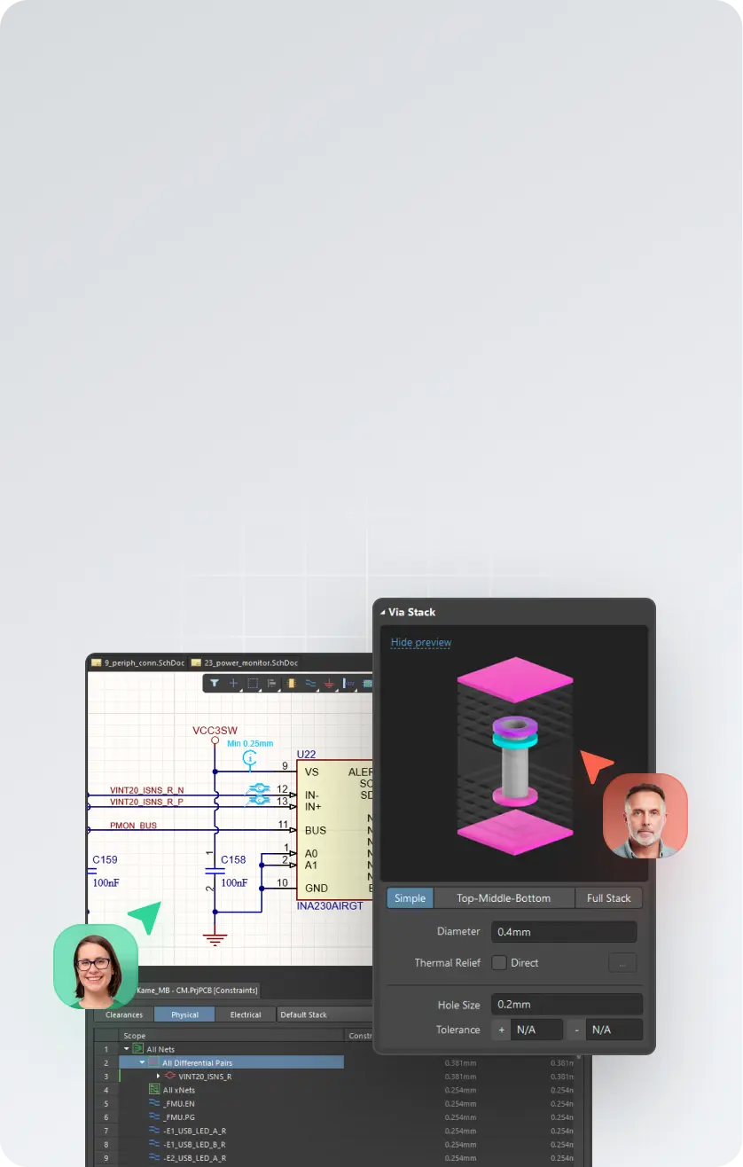
Altium Designer, optimiert für die Zusammenarbeit
Entwickelt für Einzelpersonen und kleine Teams, um zu
entwerfen, zu teilen und von überall aus synchron zu bleiben.
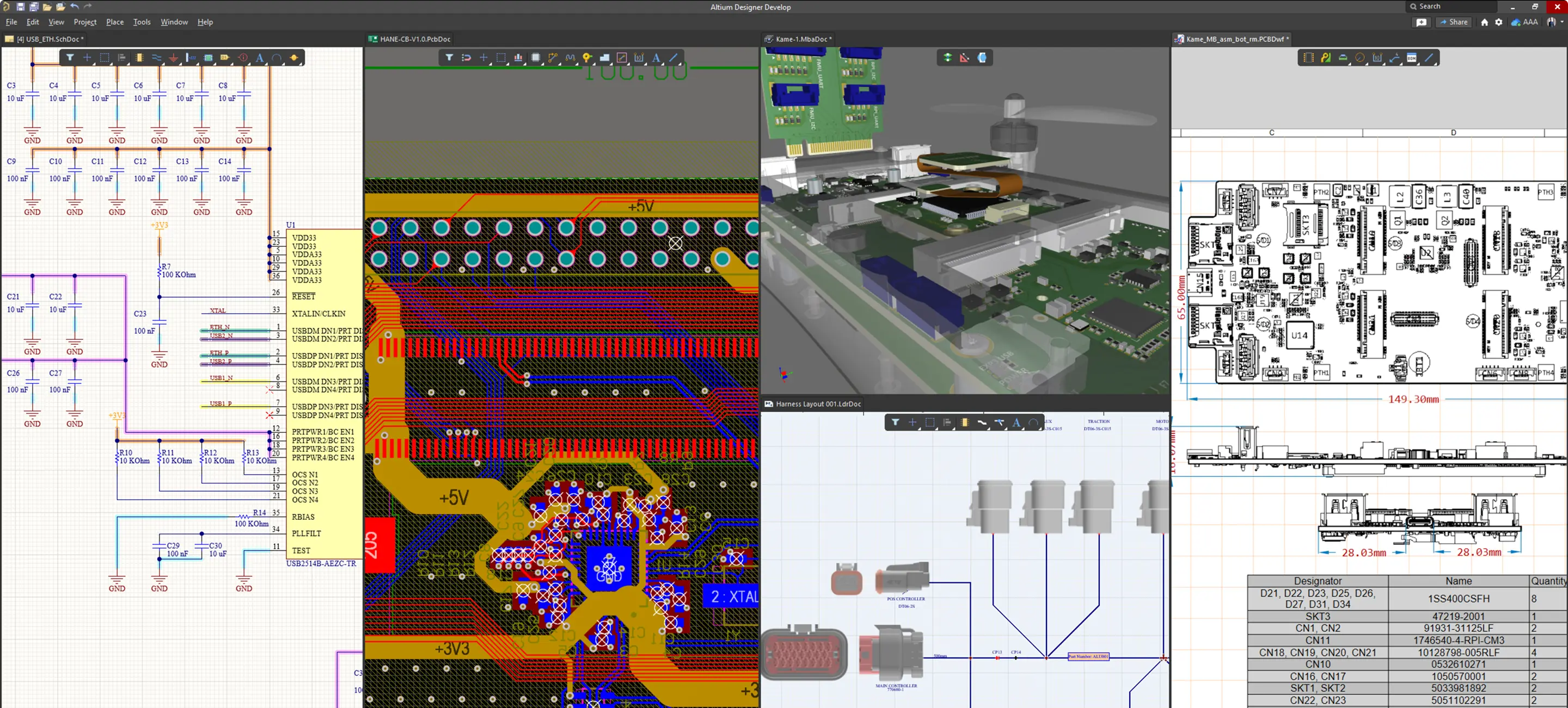
Professionelles Leiterplattendesign für die tatsächliche Leiterplattenfertigung
Altium Designer vereint alles – von Schaltplänen und Layout bis hin zu Simulation und Analyse – in einer nahtlosen Arbeitsumgebung.
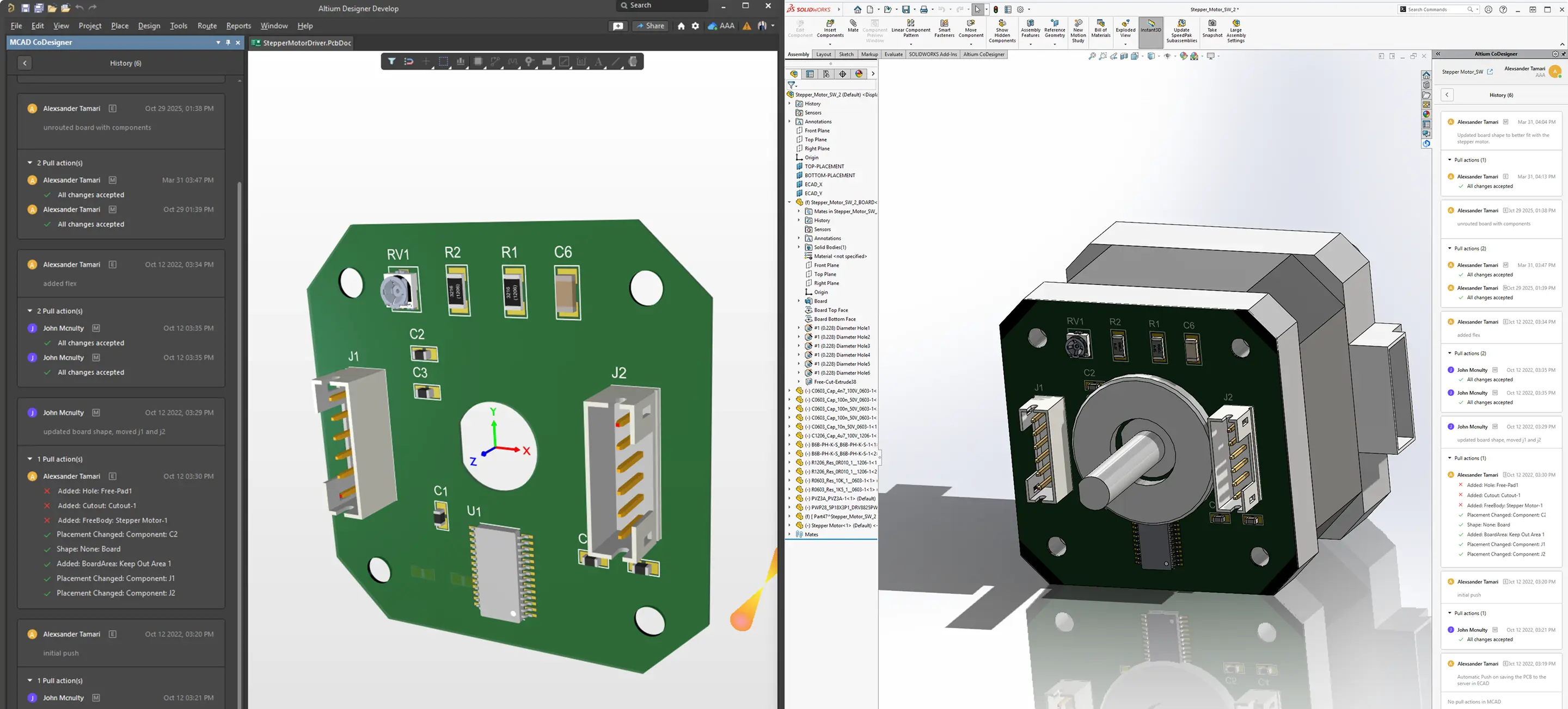
Mit MCAD zusammenarbeiten, ohne Dateien auszutauschen
Synchronisieren Sie Ihr Leiterplattendesign mit den beliebtesten MCAD-Werkzeugen. Beinhaltet die Synchronisierung von Sperrbereichen und Räumen sowie erweiterte Kupfergeometrie in MCAD.
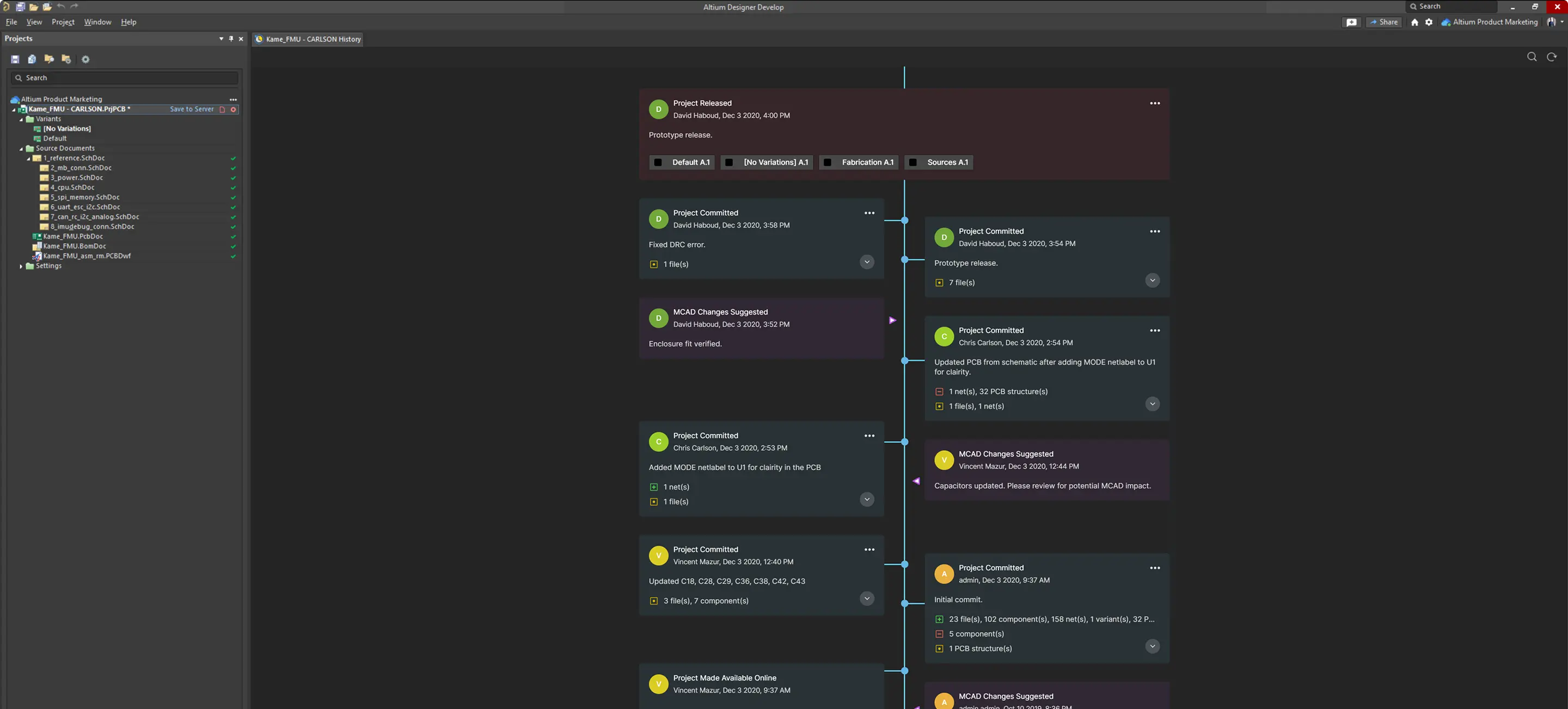
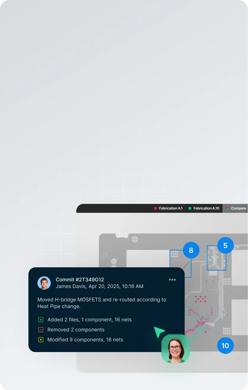
Sicherstellen, dass Revisionen und Release-Ergebnisse dem richtigen Projektstatus zugeordnet sind
Änderungen, Rückmeldungen, Teiledaten und Freigabeergebnisse bleiben mit Ihrem aktuellen Entwurfsstand verknüpft. Dadurch lässt sich leichter erkennen, was sich geändert hat, Sie können ohne zusätzliche Schritte sicher veröffentlichen und Beschaffungsrisiken frühzeitig angehen, bevor sie zu Verzögerungen führen.
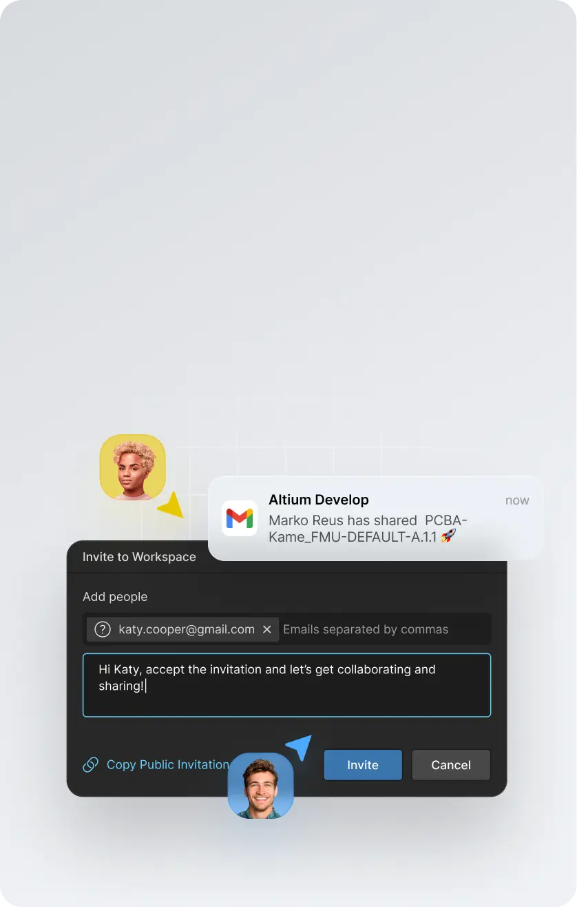
Vom Dateichaos zur vernetzten Klarheit
Verabschieden Sie sich von verstreuten Dateien und Versionschaos und steigen Sie um auf eine vernetzte Arbeitsweise –
mit Konstruktionsdaten, die stets übersichtlich, zugänglich und zuverlässig sind
Alte Methode
Designdateien sind über E-Mails, Desktops und freigegebene Ordner verstreut, was die Zusammenarbeit verlangsamt und zu ständiger Verwirrung hinsichtlich Versionen und Aktualisierungen führt.
Neuer Weg
Die Konstruktionsdaten werden in Altium 365 gespeichert, sodass Teams über einen gemeinsamen Ort verfügen, an dem sie arbeiten, Überprüfungen vornehmen und Änderungen übersichtlich nachverfolgen können.
Entwerfen in Altium Designer
Teilen und Zusammenarbeiten in Altium 365
Entwerfen, Teilen und Zusammenarbeiten in einem integrierten Arbeitsablauf
Design in Altium Designer
Erstellen von Schaltplänen, Leiterplatten-, Mehrplatten- und Kabelbaumkonstruktionen
Teilen mit
Altium 365
Zentralisieren Sie Ihre Designdaten in einem sicheren Arbeitsbereich
Zusammenarbeiten
Überall
Verfolgung von Änderungen, Vergleichen von Revisionen und Verwaltungen von Freigaben
pro Jahr
Starten Sie eine Testversion, um Altium Develop aus erster Hand kennenzulernen
Erweitere dein Team
Füge bis zu 4 weitere Altium Designer Autoren für jeweils 995$pro Jahr hinzu.
Wenn du mehr als 5 ECAD-Autoren hast, solltest du Altium Agile Teams ausprobieren, weil es besser passt.

Warum Ingenieure Altium wählen
Entwerfen, Teilen und Zusammenarbeiten in einem integrierten Arbeitsablauf
Weltweit von Innovatoren vertraut
Kostenlose 30-Tage-Testversion.Keine Verpflichtungen.
Entwirf, was immer du möchtest. Behandle es als Arbeitsablaufexperiment, nicht als Verpflichtung.
- Entwirf während der Testphase beliebige Leiterplatten/PCBs für Multi-Board-Projekte
- Keine Kreditkarte erforderlich, um zu starten
- Kein Verkaufskontakt, es sei denn, du forderst ihn an
- Optionaler technischer Support, falls du nicht weiterkommst
Kostenlos beginnen
Kostenloser Zugang für 30 Tage. Keine Kreditkarte erforderlich.
Studieren Sie? Melden Sie sich im Student Lab an