
Controlled Impedance Routing
With increasing device switching speeds, controlled impedance routing has become a hot topic for the digital designer. This page introduces how you can use the Signal Integrity analysis engine to match component impedances and the controlled impedance routing capabilities in the PCB editor.
There is a saying in engineering circles - there are only two kinds of electronics engineers working in digital design: those who have had signal integrity problems and those who will. Not so many years ago, the term signal integrity was one for the specialist, and you only had to deal with it on high-speed designs. However, the device switching speeds in those high-speed designs are no longer special; they are rapidly becoming the norm. As improving integrated circuit technology drives the size of the transistor down, the speeds at which they can switch go up. It is this switching speed that affects the integrity of digital signals.
Thankfully, many potential signal integrity issues can be avoided by following good design principles and implementing the design as a controlled impedance board. Achieving this requires specific design tool capabilities - you need analysis tools that detect nets with potential ringing and reflection issues and board design tools that allow you to achieve the correct routing impedances. The PCB editor in Altium Designer has these capabilities.
This page will help you understand what causes signal integrity issues and if your board will likely suffer from them. It will also discuss the two design approaches you must employ to minimize potential SI issues - matching component impedances, and controlled impedance routing.
When the Routing Becomes Part of the Circuit
As device switching speeds increase, so too do the demands on the printed circuit board designer and the fabricator. As the length of the signal-switching edge becomes shorter than the length of the PCB trace that carries it, the trace has to be treated as part of the circuit. That trace has an impedance, which is referred to as the characteristic impedance (Zo).
The best way to manage the impact of these additional circuit elements is to design the trace routing so that the characteristic impedance is consistent over the length - a technique called controlled impedance routing.
The impedance of the trace routing is defined by the:
- Cross-sectional area of the trace - determined from the width, the height (copper thickness), and the slope of the trace edges created during the etching process.
- Distance from the trace to the reference plane(s) - the return path of the signal energy is as important as the signal's path. This return path follows the signal path in the adjacent reference plane(s).
- Properties of the surrounding materials - the energy in the signal is not contained within the copper of the trace; due to the skin effect, it also travels down the dielectric material surrounding the trace. The permittivity of the dielectric material measures how much the dielectric impacts the flow of that energy.
 required to achieve the specified impedance.")
The Simbeor impedance calculator calculates the width(s) required to achieve the specified impedance.
Do I Need Controlled Impedance Routing?
Do I need to bother with controlled impedance routing, you ask?
In an ideal situation, all of the energy that comes out of a component output pin would be coupled into the connected track on the PCB, flow through the PCB routing to the load input pin at the other end, and be absorbed by that load. If all the energy is not absorbed by the load, then the leftover energy can be reflected back into the PCB routing, flowing to the source output pin. This reflected energy can interact with the original signal, adding to and subtracting from it (depending on the polarity of the energy), resulting in ringing. If the ringing is large enough, it will affect the integrity of the signal, resulting in unpredictable, erroneous circuit behavior.
So, how do you know if this might occur? If the source pin is able to complete its edge transition before the signal reaches the load pin, the conditions exist for your design to be impacted by reflected energy. A common rule of thumb that is used to determine if SI issues are likely is the "1/3 rise time" rule. This rule states that if the trace is more than 1/3 of a rise time long, reflections (ringing) can occur. If the source pin has a 1 nSec rise time, a route longer than .33 nSec (approximately 2 inches in FR4) must be considered a transmission line, a candidate for signal integrity issues. If your devices have this sort of rise time and you know you will have routing of this sort of length, then you might end up with signal integrity issues on the PCB.
How Do I Control the Impedances?
How do you avoid the situation where energy is reflected back and forth between the source and the load? You avoid it by matching the impedances. Impedance matching ensures that all the energy is coupled from the source into the routing and then from the routing into the load. Routing the board with regard to the impedance is referred to as controlled impedance routing or another way of saying it is that a board where impedances have been managed is called a controlled impedance PCB.
There are two distinct elements to achieving impedance matching: the first is matching the components; the second is routing the board to give the required impedance.
Impedance Matching the Components
You cannot achieve a controlled impedance PCB with routing alone. First, you must check and if necessary, match the impedances of the components.
Ideally, you want to detect nets that could have potential signal integrity issues during the design capture phase so that any additional termination components can be included before the board design process starts. Since output pins are low impedance and input pins are high impedance, it is likely that you will need to add termination components to the design to achieve impedance matching.
You can perform a signal integrity analysis on your design at the schematic capture stage. When you run the Tools » Signal Integrity command the Errors or Warnings dialog will often appear, indicating that not all components have signal integrity models assigned. The Signal Integrity analysis engine will automatically select default models based on the component designators, click Continue to use the defaults or Model Assignments to examine and change the models. You can access the Signal Integrity Model Assignments dialog anytime, via the Model Assignments button in the Signal Integrity panel.

Analyzing the Design
When the Tools » Signal Integrity command is run, the design is analyzed, and any potential problem nets are identified in the Signal Integrity panel, as shown below.
 Testing the design for potential signal integrity issues during design capture.
From the panel, you can perform a reflection analysis on a selected net (or nets). On the left are the analysis results for all nets in the design. Select a net and click the ![]() button (or double-click a net name) to transfer that net to the Net field on the right of the panel, where you can perform a detailed analysis of that net, including:
button (or double-click a net name) to transfer that net to the Net field on the right of the panel, where you can perform a detailed analysis of that net, including:
- Examining the pins in that net, where you can single-click to cross-probe to that pin on the schematic or double-click to check and configure the model assigned to that pin.
- Enable one or more theoretical termination options for that net.
- Perform a Reflection Analysis on the net, producing a set of waveforms showing the behavior at each pin in the net.
The panel allows you to experiment with possible termination configurations and values. Note that the Termination region of the Signal Integrity panel shown in the image above has the Serial Res option enabled. The section of the panel below shows a series termination resistor. This is where you define the minimum and maximum theoretical series termination resistance values that will be used for the reflection analysis (disable the Suggest checkbox to enter your own values).
Exploring the Results
When the Reflection Waveforms button clicks, an accurate reflection analysis is performed on that net, with the results presented in a new waveform window (*.SDF).
The waveform window will include:
- A Chart for each net being analyzed, click the tabs at the bottom of the window to switch between Charts.
- Each Chart will include a Plot for each pin in that net, showing signal behavior at that pin.
The images below show two graphs of the results at the input pin of the net selected in the previous panel image. The first graph is the input pin in the net without termination; the second graph shows six sweeps, one for the original unterminated net, and then five sweeps with the theoretical series termination resistance included at the source pin.
Five passes of the reflection analysis were performed (Sweep Steps option value = 5), with the theoretical termination resistor stepping from Min = 20 ohms to Max = 60 ohms. The five passes (first pass at 20 ohms, last pass at 60 ohms) are listed on the right-hand side of the graph. Clicking on each label highlights that result and displays the theoretical termination resistance value at the bottom right. For this net, a series termination resistance of 40 ohms would produce the graph selected in the image on the right.

 The graph on the left shows the reflection analysis of a net with potential signal integrity issues; the graph on the right is the same net with a theoretical series termination resistor of approximately 40 ohms added.
What Determines the Routing Impedance?
The second part of achieving a controlled impedance PCB is to route the board so that the tracks have a defined impedance. There are a number of factors that influence the impedance of your signal routing, including the dimensions of the routes and the properties of the materials used to fabricate the PCB.
The PCB editor includes the Simbeor® electromagnetic Signal Integrity engine from Simberian. Simbeor's model accuracy is validated using advanced algorithms for 3D full wave analysis, benchmarking, and experimental validation. The Simbeor engine supports all modern board structures and materials.
Simbeor Version
The Simbeor SFS
Impedances are calculated by the Simbeor SFS, a quasi-Static Field Solver. Simbeor SFS is an advanced quasi-static 2D field solver based on Method of Moments, which has been validated by convergence, comparisons, and measurements. The solver meshes dielectric and conductor boundaries and solves corresponding equations to build frequency-dependent RLGC matrices for the Telegraph equations.
Simbeor SFS is not a full-wave solver as this is not needed to evaluate the impedance, delay, or attenuation in PCB interconnects because of the quasi-TEM nature of the waves propagating there. Such waves can be accurately simulated with RLGC parameters extracted with a quasi-static 2D field solver.
A unique property of the Simbeor SFS solver is that it supports conductor roughness models. Note that it does not support a multi-layered conductor model (plating), and the roughness is common for all conductors. The solver is quasi-static because the solution does not include the high-frequency dispersion that takes place in microstrip lines (higher concentration of fields in a dielectric with higher dielectric constant at high frequencies).
► Learn more about Simberian electromagnetic signal integrity technology
Supported PCB Structures
Impedances can be calculated for the following PCB structures:
- Microstrip
- Symmetrical Stripline
- Asymmetrical Stripline
- Single and differential coplanar structures
- Multiple adjacent dielectric layers with different dielectric properties.
Configuring the PCB for Controlled Impedance Routing
Controlled Impedance routing is all about configuring the dimensions of the routes and the properties of the board materials to deliver a specific impedance. This is done in the PCB editor's Layer Stack Manager. To open the Layer Stack Manager, select Design » Layer Stack Manager from the main menus. The Layer Stack Manager opens in a document editor in the same way as a schematic sheet, the PCB, and other document types do.
The trace width required to deliver a specific impedance is calculated as part of the impedance profile, configured in the Impedance tab of the Layer Stack Manager.
Based on:
- The values of the Target Impedance, Target Tolerance and Roughness that you configure in the Impedance tab, and
-
the materials settings defined in the Stackup tab, including:
- the thickness of the signal layer,
- the thickness of the surrounding dielectric layers (the distances from the reference plane(s)), and
- the properties of the dielectric material (permittivity Dk and dissipation factor Df).
When these are correctly configured, the impedance calculator has sufficient information to calculate the following:
- Trace Width
- Calculated Impedance (Z)
- Common Mode Impedance (Zcomm)
- Impedance Deviation (Z Deviation)
- Propagation Delay (Tp)
- Inductance per unit length (p.u.l.)
- Capacitance per unit length (p.u.l.)
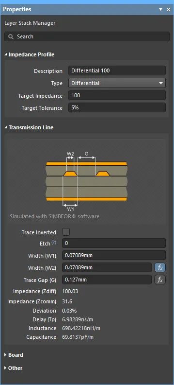
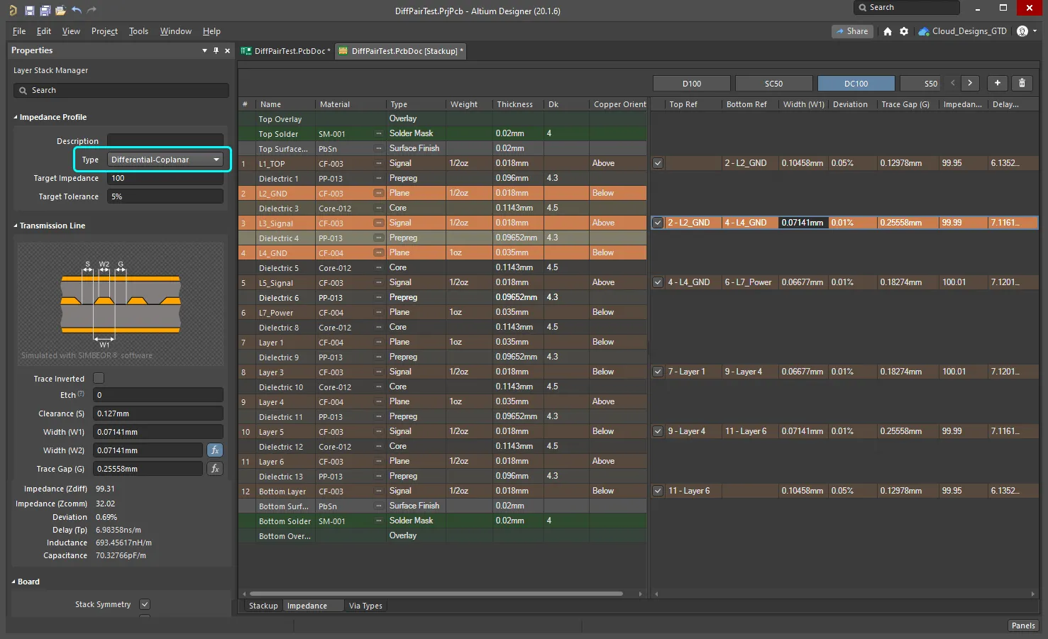
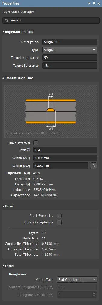
The calculated values are displayed in the Transmission Line section of the Properties panel when the Impedance tab is selected in the Layer Stack Manager, as shown below.
 A 50Ω impedance profile defined for single nets routed on the top layer. Hover the cursor over the image to display the settings for the same profile for layer L3 (image courtesy FEDEVEL Open Source, www.fedevel.com).
Configuring the Layer Stackup
Main page: Defining the Layer Stack
The copper and dielectric fabrication layers are configured on the Stackup tab of the Layer Stack Manager.
- Layers are added, removed, and configured in this tab. For a rigid-flex design, layers are also enabled and disabled in this tab.
-
The properties of the currently selected layer can be edited directly in the grid or in the Properties panel. Click the
 button at the bottom of the design space to enable the panel.
- Right-click in the layer grid or use the Edit » Add Layer commands to add a layer. Adding a copper layer will also add a dielectric layer when an existing adjacent layer is also a copper layer.
- If the Stack Symmetry option is enabled in the Board section of the Properties panel, layers are added in matching pairs centered around the mid-dielectric layer.
-
The layer Material can either be typed into the selected Material cell or selected in the Select Material dialog; click the ellipsis button (
 ) to open it.
- A surface finish can be added to a copper layer. Use the Add Layer sub-menu to add a Surface Finish layer to the currently selected copper layer, then click the ellipsis button for the new surface finish layer to select the finish type.
- The selected layer can be moved up or down within the layers of the same type using either the right-click or Edit menus.
- The Board region of the Properties panel includes options to enforce Stack Symmetry and Library Compliance. More on these below.
- The Board region of the Properties panel displays a summary of the currently selected stack (or substack for a multi-stack rigid/flex design).
Layer Stack Considerations
A fundamental requirement for controlling the impedance is to include a signal return path below each signal path. The Simbeor SI engine supports both plane layers and signal layers covered by a polygon. These return-path layers should be distributed through the board stackup. Ideally, they are arranged so that at least one return-path layer is adjacent to each signal layer carrying controlled impedance routing. The adjacent return-path layer provides the signal return path and for reasons that will not be covered here, does so regardless of the DC voltage distributed by that plane.
The return path current flowing through the plane will attempt to follow the same physical path as the route on the signal layer, so it is important to avoid introducing discontinuities, such as a split or cutout in the return-path layer underneath any critical signal routing.
As well as selecting a suitable order for signal and plane layers, you also need to define the material properties of each layer, including:
- Copper thickness
- Dielectric thickness
- Dielectric constant
These values and the routing width all contribute to the final impedance. Achieving the required impedance then becomes a process of tuning all these values. Remember that possible copper and dielectric thickness values may also be limited, determined by the materials available from your PCB fabricator.
► Learn more about possible layer stackups
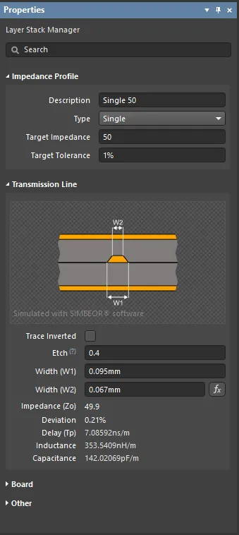
Defining the Impedance Profiles
The Simbeor engine is built into the PCB editor's Layer Stack Manager (Design » Layer Stack Manager). To configure the layer stack for controlled impedance routing, switch to the Layer Stack Manager's Impedance tab where you can add and configure an impedance profile.
A 50Ω impedance profile defined for individual nets routed on the top layer. Hover the cursor over the image to display the settings for the same profile for layer L3.
Notes on creating and configuring an Impedance Profile:
- In the Layer Stack Manager switch to the Impedance tab, as shown above.
-
Click the
 button (or the
  button if a profile is already defined) to add a new profile.
- Define the required impedance Type, Target Impedance, and Target Tolerance in the Properties panel. The Description is optional, it will be displayed wherever the Impedance Profile name is displayed.
-
The grid of layers is divided into 2 regions; the layers in the stackup are displayed on the left, then for each signal layer in the stackup, there is a layer displayed in the Impedance Profile region on the right. Use the layer checkbox in the Profile region to enable impedance calculation for that layer. Using the image above as an example and referring to the layer number shown in the left-most column, layers
L1,L3,L10andL12have their layer checkbox ticked, enabling them for impedance calculations. -
When you click on an enabled layer in the Profile region, all layers in the layer stack will fade except those being used to calculate the impedance for that selected signal layer (as shown in the image above). Edit that layer's reference layer(s) in the Impedance Profile region's Top Ref and Bottom Ref columns. Note that reference layer(s) can have a layer Type of either
Planeor Signal. For example, in the image above, layerL10in the stackup is enabled for impedance calculations, with the Top Ref set to9-L9, which is aPlanelayer, and the Bottom Ref set to11-L11, which is a Signal layer. The software assumes that if a signal layer is being used as a reference plane, it contains a continuous plane of copper connected to a power or ground net. - Enable the Impedance Profile checkbox for each other layer that will carry routing at this impedance and configure the reference plane(s). Hover the cursor over the image above to display the S50 Impedance Profile for layer L3.
- If the calculated routing trace width is a value that cannot be ordered, you can tune the width and gap settings.
Tuning the Width and Gap Settings
The software calculates the Trace Width from the target impedance and tolerance. It is not uncommon that the calculated trace width will be a value that cannot be ordered, for example, 0.0683mm. The fabricator will advise what material thicknesses are available and what precision they can achieve for trace widths. Then, it becomes a process of starting at the desired values and then testing the impact on the calculated impedance values when the dimensions are adjusted to what is available.
To support this process of testing and tuning the settings, the impedance calculators support forward and reverse impedance calculations. The default mode is forward (enter the impedance, the software calculates the width). The ![]() icon indicates the calculated variable.
icon indicates the calculated variable.

 A Target Impedance of 50Ω gives a forward calculated width (W1) of 94.6µm. The image on the right shows the reverse calculation when the width (W1) is set to 95µm.
To reverse the calculation and explore different trace widths for the selected layer, type in the new Width (W1) value and press Enter on the keyboard. The calculated values will update to reflect the impact of changing to that width. Click the ![]() button to return the calculator to forward calculation mode. Entering a new value into Width (W2) will change the Etch value.
button to return the calculator to forward calculation mode. Entering a new value into Width (W2) will change the Etch value.
To explore the differential pair transmission line results, nominate the calculated variable - either the Trace Width or Trace Gap - by clicking the appropriate ![]() button. Edit the other variable to change the Target Impedance, or alternatively change the Target Impedance to explore the impact on the other variable.
button. Edit the other variable to change the Target Impedance, or alternatively change the Target Impedance to explore the impact on the other variable.
Etch Factor
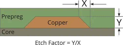
The signal traces on a PCB are fabricated by etching away unwanted copper. Because the etchant starts etching away the copper at the surface, this copper spends more time in contact with the etchant. The result is the finished edges of the trace will have a slope, reducing the cross-sectional area of the finished trace, as shown in the image below.
The area of trace-edge copper lost (on both edges) during etching = X * Y
The amount of slope is referred to as the Etch Factor, where:
Etch Factor = Y/X
If Y = X, then the Etch Factor = 1
Referring to the image shown in the Properties panel:
 Hover the cursor over the ? to show the formula.
The standard definition for Etch Factor is to specify it as the ratio of trace thickness / amount of over-etching. This gives the following formula:
Etch Factor = T/[0.5(W1-W2)]
The downside of this approach is that to specify no over-etching (meaning the trace edges are vertical), you would have to enter a value of inf (infinite) for the etch factor. To simplify specifying the amount of etch, the formula has been inverted so a value of 0 (zero) can be entered to indicate there is no over-etching.
Etch = [0.5(W1-W2)]/T
Copper orientation
Another fabrication detail that contributes to the etch factor is the orientation of the copper. PCB traces are formed by etching away unwanted copper from a continuous sheet of copper laminated onto a dielectric substrate. The copper orientation defines the direction the copper projects away from that substrate. You can also think of it as the direction the copper is etched from, either above or below.

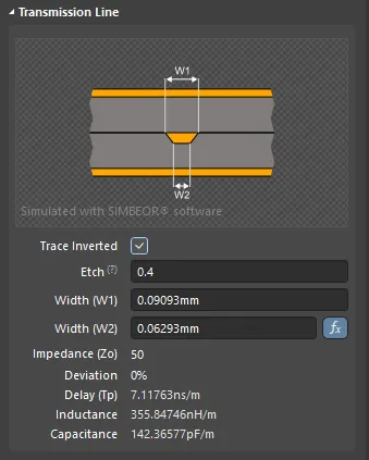 Click the Trace Inverted checkbox to toggle the Copper Orientation from Above to Below.
Conductor Surface Roughness
The surface of each copper layer in a printed circuit board has a degree of roughness. During PCB fabrication, the surface of copper layers is treated to increase the roughness to improve the adhesion between the copper and dielectric layers. This surface roughness becomes a significant contributor to conductor impedance at switching speeds above 10 GB/s. Through extensive research and analysis, industry experts have concluded that the surface roughness can be modeled by a roughness correction coefficient derived from Surface Roughness and Roughness Factor values.
Roughness settings are available in the Layer Stack Manager mode of the Properties panel. These parameters are used only for conductive layers.
 Surface roughness is included in the calculation of the characteristic impedance.
Roughness:
-
Model Type - preferred model for calculating the impact of surface roughness (refer to the articles below for more information on the various models). Applies to all copper layers in the substack.
-
Surface Roughness - value of the surface roughness (available from your fabricator). Enter a value between 0 to 10µm, default is 0.1µm
-
Roughness Factor - characterizes the expected maximal increase in conductor losses due to the roughness effect. Enter a value between 1 and 100; the default is 2.
Further reading
- Practical methodology for analyzing the effect of conductor roughness on signal losses and dispersion in interconnects: Y. Shlepnev, C. Nwachukwu, DesignCon2012.
- Unified approach to interconnect conductor surface roughness modeling: Y. Shlepnev, 2017 IEEE 26th Conference on Electrical Performance of Electronic Packaging and Systems (EPEPS2017)
Support for Coplanar Transmission Line Structures
The impedance calculator in the Layer Stack Manager supports single and differential coplanar structures. Create a new impedance profile, then select Single-Coplanar or Differential-Coplanar from the Impedance Profile Type drop-down list.
Working with coplanar structures:
- As with the standard single and differential impedances, values for each variable are automatically calculated based on the user-defined Target Impedance and Target Tolerance and the physical properties of the board layers. These automatically calculated values can be adjusted by entering new values into the edit boxes of the Layer Stack Manager mode of the Properties panel.
- To target the signal nets you want to be routed with a coplanar structure, configure a Routing Width (or Differential Pairs Routing) design rule with the Use Impedance Profile option enabled and the required Coplanar Impedance Profile selected.
- Coplanar structures require a reference plane on both sides of the signal route; this can be created by a polygon you place or if stitching vias are added, by the Add Shielding to Net command (more info below). If you place a polygon, the separation between this polygon and the signal route is defined by the Clearance (S) value determined by the Simbeor impedance calculator (displayed in the Properties panel, shown in the images above and below). Configure a Clearance design rule to control the clearance between the reference polygon and the signal route (show image).
-
It is common practice to include a via fence along each side of the signal trace when the coplanar structure is grounded. Use the Tools » Via Stitching/Shielding » Add Shielding to Net command in the PCB editor to do this. As well as placing vias, by enabling the Add shielding copper option this command can also place a polygon around the signal routing to cover the via fence, as shown in the image on the right below.
► Learn more about Via Shielding

, use that clearance in the via shielding Distance setting.")
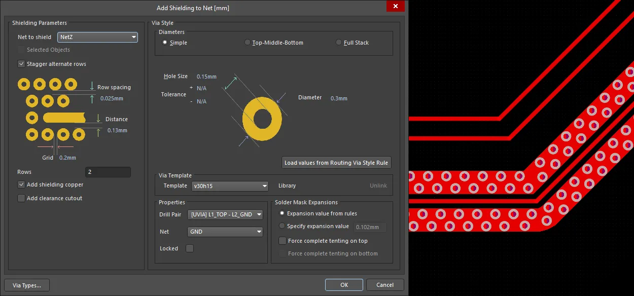 The impedance calculator determines the signal properties and clearances (first image), use that clearance in the via shielding Distance setting.
Selecting the Layer Material
In a controlled impedance design, selecting the materials used in the layer stackup is very important.
For example, the most common material for fabricating PCBs is glass fiber (fiberglass) reinforced epoxy resin, with copper foil bonded onto each side. The tightness of the weave of the glass fiber fabric affects the value and consistency of the dielectric constant Dk (permittivity) and Loss Tangent Df. Surrounding the woven glass fabric is resin - the percentage of resin used is also important in the performance of the material.
There is a large range of glass fiber weaves available. To help ensure the predictability and performance of the glass fiber-based materials used in PCB fabrication, the IPC has a standard for weaves:
IPC standard IPC-4412B: Specification for Finished Fabric Woven from "E" Glass for Printed Boards
The Material Library
As the designer, you can either edit the material properties directly in the Layer Stack Manager or select materials from the Altium Material Library.
The entire library can be viewed (and added to) in the Altium Material Library dialog (Tools » Material Library).
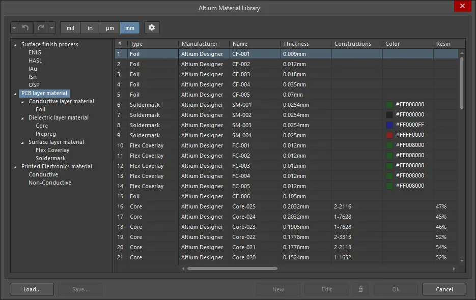
The materials are organized into usage categories, accessed through a tree structure on the left of the dialog. Below this level, each usage category is broken into functional categories, such as Conductive layer material, Dielectric layer material, and Surface Layer Material in the PCB layer material category.
Adding, Saving and Loading Material
New material can be added to the library when a specific material category is selected in the tree. Materials defined in an external material library can be loaded (Load button), and user-defined material that has been added in the Altium Material Library dialog can also be saved to a user library (Save button). Only user-defined material is saved.
Adding Custom Properties to Material
Custom properties can be added to material detailed in the library (default and user-defined material). To add a custom property, first select the correct node in the tree on the left to define the material(s) it is to be added to, then click the ![]() button to open the Material Library Settings dialog.
button to open the Material Library Settings dialog.
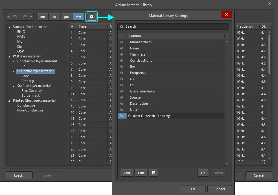
The required value can then be added to the selected material in the Altium Material Library dialog; select the row and click the Edit button.
Properties Panel
When the Impedance tab of the Layer Stack document is active, the Properties panel allows you to configure the Impedance Profile requirements. The required Impedance Profile can then be selected in the Routing Width or Differential Pairs Routing design rules.
-
Impedance Profile
- Description – enter a meaningful description. This field is optional and will be displayed wherever the Impedance Profile name is displayed.
- Type – use the drop-down to choose the impedance type. Choices are Single, Differential, Single-Coplanar, and Differential-Coplanar.
- Target Impedance – enter the impedance you want to achieve.
- Target Tolerance – enter the tolerance you want to achieve. You should consult with the fabricator to find a realistic value for tolerance that the fabricator can deliver.
-
Transmission Line
- Trace inverted – enable this option to invert the trace, as demonstrated in the Properties panel. This option is the same as the Copper Orientation option displayed when the Stackup tab is active and defines the direction in which the copper is laminated onto the core. The copper orientation defines the direction the copper projects away from that substrate. You can also think of it as the direction the copper is etched from, either above or below.
-
Etch – the Etch Factor is
= T/[(W1-W2)/2], which reduces the total cross-section area of the trace by the thickness of the copper squared. Consult the board fabricator for information about the Etch created by their processes.
-
Width (W1) / (W2) – W1 is the width of the trace you route, W2 is the width of the upper surface of that trace once it has been etched, with the Etch factor applied. There is a forward/reverse calculation feature available for trace width. The default is for the width to be calculated based on the Target Impedance you entered (forward calculation). That width may be a value that the fabricator may not be able to deliver, such as 5.978, and they will want a more sensible value, such as 6.0. You can enter 6.0 into the Width field and press Enter on the keyboard to recalculate the calculated values (Impedance, Deviation, etc.). The
 button turns gray (becomes inactive) and you are now in reverse calculation mode. If you click the button to make it active, you are again in forward mode, and the Width (W1) will revert to the calculated value. This feature lets you explore realistic fabricate-able width options. Manually entering a value for W2 will update the etch factor to suit.
- Impedance – the software calculates the impedance based on the properties of the materials used to make the board (copper, core and prepreg) and the cross-sectional area of the trace (determined by the width, thickness and etch factor of the trace).
- Deviation – this is a measure of the difference between what you wanted (target impedance) and what you got (calculated impedance). The software calculates the impedance deviation (what you will actually get based on the material and dimensions entered) based on the properties of the materials used to make the board (copper, core and prepreg) and the cross-sectional area of the trace (determined by the width, thickness and etch factor of the trace).
- Delay – this is the amount of time it takes for the signal to travel from the sender to the receiver.
- Inductance – the impedance calculator uses the Impedance value to calculate the inductance per unit length.
- Capacitance – the impedance calculator uses the Impedance value to calculate the capacitance per unit length.
-
Board
- Stack Symmetry – enable to add layers in matching pairs centered around the mid-dielectric layer. When enabled, the layer stack is immediately checked for symmetry around the central dielectric layer. If any pair of layers that are equidistant from the central dielectric reference layer are not identical, the Stack is not symmetric dialog opens.
- Library Compliance – when enabled, for each layer that has been selected from the Material Library, the current layer properties are checked against the values of that material definition in the library.
- Substack – this information is for the currently selected substack (layers, dielectric, thicknesses, etc.). As you switch from one substack to another, this information will update accordingly (for the currently selected substack).
- Stack Name – enter a meaningful substack name. This field is useful when the X/Y stackup region is being assigned a layer substack.
- Is Flex – enable if the substack is flex.
- Layers – the total number of layers.
- Dielectrics – the total number of dielectrics.
- Conductive Thickness – the thickness of conductive layer(s). Copper signal layers are referred to as conductive layers.
- Dielectric Thickness – the thickness of dielectric layer(s).
- Total Thickness – the total thickness of the board.
- Other
-
Roughness – shows the roughness of conductive layers.
- Model Type – preferred model for calculating the impact of surface roughness (refer to the articles below for more information on the various models). Applies to all copper layers in the stack (should it be the substack?).
- Surface Roughness – value of the surface roughness (available from your fabricator). Enter a value between 0 to 10µm, default is 0.1µm
- Roughness Factor – characterizes the expected maximal increase in conductor losses due to the roughness effect. Enter a value between 1 and 100; the default is 2.
Configuring the Design Rules
The routing impedance is determined by the width and height of the route and the properties of the surrounding dielectric materials. Based on the material properties defined in the Layer Stack Manager, the required routing widths are calculated when each impedance profile is created. Depending on the material properties, the width may change as the routing layer changes. This requirement changes widths as you change routing layers is automatically managed by the applicable routing design rule configured in the PCB Rules and Constraints Editor (Design » Rules).
For most board designs, a specific set of nets will be routed with a controlled impedance. A common approach is to create a net class or differential pair class that includes these nets and then create a routing rule that targets this class, as shown in the images below.
Normally, you manually define the Min, Max, and Preferred Widths, either in the upper constraint settings to apply them to all layers or individually for each layer in the layer grid. For controlled impedance routing, you enable the Use Impedance Profile option instead, then select the required Impedance Profile from the drop-down. When this is done, the Constraints region of the rule will change. The first thing you will notice is that the available layers region will no longer show all signal layers on the board. It will now only show the layers enabled in the selected Impedance Profile. The Preferred Width values (and diff pair gap) will update to reflect the widths (and gaps) calculated for each layer. These Preferred values cannot be edited but the Min and Max values can. Set these to suitable smaller/larger values. The nets can then be interactively routed in the usual way.
Routing Width Design Rule
For single-sided nets, the routing width is defined by the Routing Width design rule.
 When you choose to Use an Impedance Profile, the available layers and Preferred Widths are controlled by the selected profile.
Differential Pairs Routing Design Rule
The routing of differential pairs is controlled by the Differential Pair Routing design rule.
 For a differential pair, the available layers, the Preferred Width and the Preferred Gap are controlled by the selected profile.
► Learn more about Differential Pair Routing
Return Path Design Rule
Breaks or necks in the return path can be detected by the Return Path design rule. The Return Path design rule checks for a continuous signal return path on the designated reference layer(s) above or below the signal(s) targeted by the rule. The return path can be created from fills, regions, and polygon pours placed on the reference signal layer or a plane layer.
The return path layers are the reference layers defined in the Impedance Profile selected in the Return Path design rule. These layers are checked to ensure the specified Minimum Gap (width beyond the signal edge) exists along the signal's path. Add a new Return Path design rule in the High Speed rule category.
 is defined by the Minimum Gap.") The return path layers are defined in the selected Impedance Profile, and the path width (beyond the signal edge) is defined by the Minimum Gap.
The return path layers are defined in the selected Impedance Profile, and the path width (beyond the signal edge) is defined by the Minimum Gap.
The image below shows return path errors detected for the signal, NetXwith a Minimum Gap setting of 0.1mm. It can be easier to locate Return Path errors by configuring the DRC Violation Display Style to show Violation Details but not the Violation Overlay ( show image) in the Preferences dialog. Doing this highlights the exact locations where the rule has failed rather than the entire object(s) in violation.


► Learn more about High Speed Design in Altium Designer
Routing Nets at the Required Impedance
As you route the board and change layers, the software will automatically adjust the track width to the size needed to achieve the specified impedance. This interactive controlled impedance routing greatly simplifies the task of designing a controlled impedance PCB.
Length Tuning the Routes
Two of the core challenges with routing a high-speed design are controlling the impedance of the routes and matching the lengths of critical nets. Impedance-controlled routing ensures that the signal that leaves an output pin is correctly received by the target input pins. Matching the route lengths ensures that timing-critical signals arrive at their target pins at the same time. Tuning and matching route lengths is also an essential ingredient of differential pair routing.
 Accordion patterns have been added to the routing to ensure that the differential pairs have matched lengths.
The Interactive Length Tuning and Interactive Diff Pair Length Tuning commands (Route menu) provide a dynamic means of optimizing and controlling net or differential pair lengths by allowing variable amplitude wave patterns (accordions) to be inserted according to the available space, rules and obstacles in your design.
► Learn more about Length Tuning
Testing the Signal Integrity of the Routed Board
In the same way that you tested the nets during design capture using an assumed routing length and routing impedance, once the routing is complete, you should repeat this process on the board to check for potential impedance mismatches and reflection issues. Launch the Signal Integrity command from the PCB editor Tools menu. Since the PCB is part of the project, the material properties and dimensions defined in the Layer Stack Manager and the actual widths of the routes on the board will be used to calculate the impedances used for the signal integrity tests.
Achieving the Specified Impedances
Beyond the iterative dimension tuning process that you go through to achieve the correct impedances, there are other factors that influence the final impedance that will be achieved on your fabricated PCB. These include the consistency and stability of the dielectric material used in the PCB and also the consistency and quality of the etching process. If you require a controlled impedance PCB, you should discuss this with your PCB fabricator. Some fabricators can advise on track geometries if you supply them with your preferred stackup. Many will also be able to include an impedance test coupon on each panel that they fabricate - this can be used to measure the real impedances achieved on the board.
Additional Reading and Resources
This article gives an introduction to the topic of signal integrity and controlled impedance PCB design. Use the following links to learn more and access resources developed by recognized industry experts.