A Keepout in PCB design is a user-defined area or perimeter placed in the layout that copper objects cannot intersect. Typically included to control the area used by automated copper placement actions, such as polygon pours and interactive routing, a Keepout also represents an invalid location when manually placing copper objects.
As specified ‘no go’ areas during design layout, Keepout objects use the existing Clearance Constraint Rules to control routing and detect placement violations, but unlike other placed objects, cannot be assigned to a Net and are not shown in generated Outputs or printouts. In its simplest sense, a Keepout acts as an ‘interference’ object that prevents other copper objects from intersecting its area, as specified by the global Clearance Rule. Keepout objects can be placed on the Keep-out Layer (where they apply to all signal layers), or they can be placed on a signal layer (where they only apply to objects on that layer).
Altium Designer allows for the creation and application of Keepouts with its support for Object Specific Keepouts. Placed Keepout objects can be configured to specify which type objects they apply to, such as tracks, copper areas, vias, and pads, which significantly enhances the flexibility and effectiveness of Keepouts.
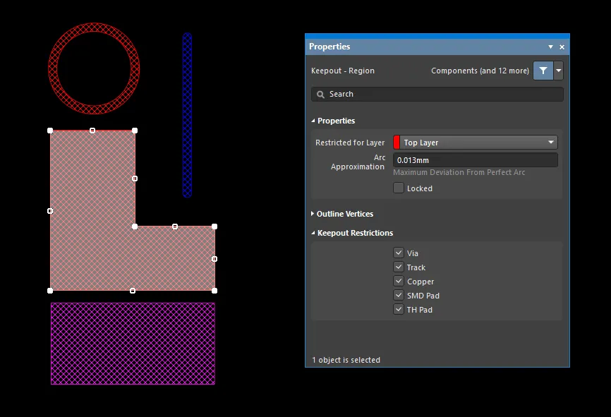
Keepout objects of different types placed in a PCB design.
In the PCB and PCB Library Editor, Keepout objects are displayed with cross-hatching. Keepout objects placed on the Keep-Out Layer (i.e. applies to all signal layers) are shown in the Keep-Out Layer color, whereas Keepouts placed on a specific signal layer (i.e. applies to that signal layer only) appear in the color of that signal layer.
Keepouts are ideal for defining non-routable board regions (such as electrically sensitive or high voltage areas), specifically exposed copper locations such as in Fiducials and Test Points, or mechanically incompatible areas (such as mounting holes or the corners of a PCB). The configurable nature of Object Specific Keepouts also allows them to be placed over other objects when specific Keepout Restrictions have been assigned. When set to restrict only Vias, for example, a Keepout can be placed over existing copper regions (such as a Polygon Pour) to control the extent of automated Via Stitching.
Object Specific Keepouts can be placed in the PCB Editor and PCB Library Editor.
For more information on placing and editing PCB keepout objects, refer to the collapsible sections below:
Track Keepout

A placed Track Keepout
A track is a primitive design object. As well as the standard track that is used for design tasks, there is a second type of track available, referred to as a track keepout. A track keepout can be placed as a layer-specific keepout object or an all-layer keepout to act, for example, as a placement or routing barrier. The difference between a standard track and a track keepout is that layer-specific keepout-type fills are not included in output generation, such as Gerber or ODB++. A keepout region is identified by having an outline in the Keepout color.
A keepout track can only be placed on a signal layer or the Keepout layer.
After launching the track keepout placement command, the cursor will change to a cross-hair and you will enter track keepout placement mode. Placement is made by performing the following sequence of actions:
- Click or press Enter to anchor the starting point for the first track keepout segment.
- Move the cursor to define the track keepout segment then click or press Enter to anchor the end point for this first segment, which is also the start point for the next connected segment.
- Continue to position the cursor then click or press Enter to anchor a series of vertex points that define the series of connected track keepout segments.
- Right-click or press Esc to end the current series of connected track keepout segments.
Additional actions that can be performed during placement include:
- Press the * key on the numeric keypad to cycle through the available signal layers. Alternatively, use the Shift+Ctrl+Wheel Roll combination to move through the routing layers; each notch of the mouse wheel will move to the next (or previous) available signal layer.
- Press the + and - keys on the numeric keypad to cycle forward and backward through all layers currently visible in the design.
While placing keepout track segments there are five available corner modes, four of which also have corner direction sub-modes. During placement:
- Press Shift+Spacebar to cycle through the five available corner modes.
- Press Spacebar to toggle between the two corner direction sub-modes.
- When in either of the arc corner modes, hold the , or . keys to shrink or grow the arc. Hold the Shift key as you press to accelerate arc resizing.
- Press the 1 shortcut key to toggle between placing one segment per click or two segments per click. In the first mode, the hollow track segment is referred to as the look-ahead segment.
- Press the Backspace key to remove the last vertex.
The graphical method of editing allows you to select a placed track keepout object directly in the design space and graphically change its size, shape or location.
When a track keepout is selected, the following editing handles are available:

- Click the end handles to reposition the end points of the track.
- Click and drag the center handle to change the shape of the track.
Track Keepout Properties

The Keepout - Track mode of the Properties panel.
Location
- (X/Y)
- X (first field) - the current X (horizontal) coordinate of the reference point of the track keepout relative to the current origin. Edit to change the X position of the track keepout. The value can be entered in either metric or imperial; include the units when entering a value whose units are not the current default.
- Y (second field) - The current Y (vertical) coordinate of the reference point of the track keepout relative to the current origin. Edit to change the Y position of the track keepout. The value can be entered in either metric or imperial; include the units when entering a value whose units are not the current default.
Properties
- Component – this field is shown in the PCB editor only when the selected Track Keepout is a constituent part of a PCB Component and displays the designator of the parent PCB component. Select the clickable Component link to open the Component mode of the Properties panel for the parent component.
- Restricted for Layer - use the drop-down to select the restricted layer.
- Width - displays the current width of the track keepout. Edit this field to change the track keepout width within the range 0.001mil to 10000mil.
- Start (X/Y) - displays the current X/Y coordinate of the track keepout start point relative to the current origin.
- End (X/Y) - displays the current X/Y coordinate of the track keepout end point, relative to the current origin.
- Length - displays the current length of the track keepout. Edit this field to change the track keepout length within the range 0.001mil to 10000mil.
Values can be defined in either mm or mil units. When entering a value in units other than the current units, add the mm or mil suffix to the value.
Keepout Restrictions
Use this region to select which object types will be restricted by the Keepout. Deselecting an object type will cause the Keepout to allow transgressions by that type of object (not kept out) by not imposing the applicable Clearance Rule. Choices include:
- Via
- Track
- Copper
- SMD Pad
- TH Pad
Arc Keepout
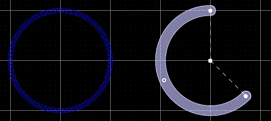
Two bottom layer Keepout Arcs: on the left is a Full Circle Keepout Arc; on the right is a Keepout Arc selected for editing.
An arc keepout is a primitive design object. It is essentially a circular track segment that can be placed on any layer. As well as the standard arc that is used for design tasks such as defining a component outline or curved routing, there is a second type of arc available, referred to as a keepout arc. A keepout arc can be placed on a signal layer to create a layer-specific barrier or no-go region. They also can be placed on the Keepout layer where they will apply to all signal layers. The difference between a standard arc and a keepout arc is that layer-specific keepout-type arcs are not included in output generation, such as Gerber or ODB++. A keepout arc is identified by having an outline in the Keepout color.
A keepout arc can only be placed on a signal layer or the Keepout layer.
The way in which an arc is placed depends on the particular method of placement that you have chosen to invoke. Four different methods of arc placement are supported:
- Place arc by center – this method enables you to place an arc object using the arc center as the starting point.
- Place arc by edge – this method enables you to place an arc object using the edge of the arc as the starting point. The arc angle is fixed at 90°.
- Place arc by edge (any angle) – this method enables you to place an arc object using the edge of the arc as the starting point. The angle of the arc can be any value.
- Place full circle arc – this method enables you to place a 360° (full circle) arc.
Placing a Keepout Arc Starting at the Center
After launching the command, the cursor will change to a cross-hair and you will enter keepout arc placement mode. Placement is made by performing the following sequence of actions:
- Click or press Enter to anchor the center point of the keepout arc.
- Move the cursor to adjust the radius of the keepout arc then click or press Enter to set it.
- Move the cursor to adjust the start point for the keepout arc then click or press Enter to anchor it.
- Move the cursor to change the position of the keepout arc's end point then click or press Enter to anchor it and complete placement of the keepout arc.
- Continue placing further keepout arcs or right-click or press Esc to exit placement mode.
Placing a Keepout Arc Starting at the Edge
After launching the command, the cursor will change to a cross-hair and you will enter keepout arc placement mode. Placement is made by performing the following sequence of actions:
- Click or press Enter to anchor the start point for the keepout arc.
- Move the cursor to change the position of the keepout arc's end point then click or press Enter to anchor it and complete placement of the keepout arc.
- Continue placing further keepout arcs or right-click or press Esc to exit placement mode.
Placing a Keepout Arc Starting at the Edge (any angle)
After launching the command, the cursor will change to a cross-hair and you will enter keepout arc placement mode. Placement is made by performing the following sequence of actions:
- Click or press Enter to anchor the start point for the keepout arc.
- Move the cursor to adjust the radius of the keepout arc then click or press Enter to anchor the center point.
- Move the cursor to change the position of the keepout arc's end point then click or press Enter to anchor it and complete placement of the keepout arc.
- Continue placing further keepout arcs or right-click or press Esc to exit placement mode.
Placing a Full Circle Keepout Arc
After launching the command, the cursor will change to a crosshair and you will enter keepout arc placement mode. Placement is made by performing the following sequence of actions:
- Click or press Enter to anchor the center point of the keepout arc.
- Move the cursor to adjust the radius of the keepout arc then click or press Enter to set it and complete placement of the keepout arc.
- Continue placing further keepout arcs or right-click or press Esc to exit placement mode.
For all methods (excluding full circle arcs), press the Spacebar before defining the keepout arc's end point to render the arc in the opposite direction.
The graphical method of editing allows you to select a placed arc object directly in the design space and graphically change its size, shape or location.
When a keepout arc object is selected, the following editing handles are available:
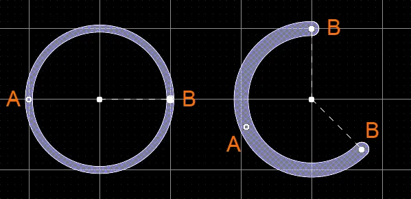
A selected Keepout Arc
- Click and drag A to adjust the radius.
- Click and drag B to adjust the end points (start and end angles).
- Click anywhere on the arc away from editing handles then drag to reposition it. Alternatively, click and drag on the arc center-point. While dragging, the arc can be rotated or mirrored:
- Press the Spacebar to rotate the arc counterclockwise or Shift+Spacebar for clockwise rotation. Rotation is in accordance with the value for the Rotation Step defined on the PCB Editor – General page of the Preferences dialog.
- Press the X or Y keys to mirror the arc along the X-axis or Y-axis respectively.
Arc Keepout Properties
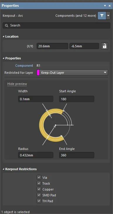
The Keepout - Arc mode of the Properties panel.
Location
- (X/Y)
- X (first field) - the current X (horizontal) coordinate of the reference point of the arc keepout, relative to the current design space origin. Edit to change the X position of the arc keepout. The value can be entered in either metric or imperial; include the units when entering a value whose units are not the current default.
- Y (second field) - The current Y (vertical) coordinate of the reference point of the arc keepout, relative to the current origin. Edit to change the Y position of the arc keepout. The value can be entered in either metric or imperial; include the units when entering a value whose units are not the current default.
Properties
- Component – this field is shown in the PCB editor only when the selected Arc Keepout is a constituent part of a PCB Component and displays the designator of the parent PCB component. Select the clickable Component link to open the Component mode of the Properties panel for the parent component.
- Restricted Layer - this field displays the restricted layer to which the arc keepout is currently assigned. To change the layer, click the field and select a layer from the drop-down list.
- Width - this field displays the width of the arc keepout line. Enter a different value for the width if required.
- Radius - this field displays the radius of the arc measured from the center point to the center of the arc keepout line. Enter a different value for the radius if required.
- Start Angle - this field displays the start angle of the arc keep out measured from the X-axis in the first quadrant (plane geometry). Enter a different value for the start angle if required.
- End Angle - this field displays the end angle of the arc keepout. Enter a different value for the end angle if required.
Values can be defined in either mm or mil units. When entering a value in units other than the current units, add the mm or mil suffix to the value.
Keepout Restrictions
Use this region to select which object types will be restricted by the Keepout. Deselecting an object type will cause the Keepout to allow transgressions by that type of object (not kept out) by not imposing the applicable Clearance Rule. Choices include:
- Via
- Track
- Copper
- SMD Pad
- TH Pad
Region Keepout

A Region Keepout
A region keepout is a primitive design object. As well as the standard region that is used for design tasks, there is a second type of region available, referred to as a region keepout. A region keepout can be placed as a layer-specific keepout object or an all-layer keepout to act, for example, as a placement or routing barrier. The difference between a standard region and a keepout region is that layer-specific keepout-type fills are not included in output generation, such as Gerber or ODB++. A keepout region is identified by having an outline in the Keepout color.
A region keepout can only be placed on a signal layer or the Keepout layer.
After launching the region keepout placement command (Place » Keepout » Solid Region), the cursor will change to a cross-hair and you will enter region keepout placement mode. Placement is made by performing the following sequence of actions:
- Position the cursor then click to anchor the starting vertex for the region keepout.
- Move the cursor ready to place the second vertex. The default behavior is to place two edges with each click, with a user-defined corner shape between them.
- Continue to move the mouse and click to place further vertices.
- After placing the final vertex, right-click or press Esc to close and complete placement of the region keepout. There is no need to manually close the region since the software will automatically complete the shape by connecting the start point to the final point placed.
- Continue placing further region keepouts or right-click or press Esc to exit placement mode.
The graphical method of editing allows you to select a placed object directly in the design space and graphically change its size, shape or location.
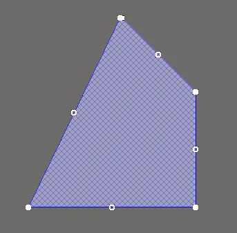
A selected Region Keepout
Move Region Vertices
Region Keepouts contain two points, or "handles", with which to edit the shape of the region.
- Full Handles - located at the corners of the region keepout.
- Empty Handles - located in the centers of the segments created by the Full Handles.
An existing region keepout can be re-shaped by moving these handles, or vertices, located at each corner or at the center of each edge.
To modify the region keepout shape:
- Click and select a region keepout, which will highlight the vertices for the region keepout and change the cursor to a crosshair.
- Click on a Full Handle to move that corner.
- Click along an edge to move the entire edge.
- Click on an Empty Handle to move the whole side (for track and for arc).
- Ctrl+Click on an Empty Handle to break that edge into two edges. Ctrl only needs to be held at the beginning of movement. The Shift+Spacebar hotkeys can then be used to cycle through modes (arc, miter, and any angle).
- If the 'any angle' placement mode creates unwanted vertices, or to remove extra vertices in general, click Ctrl and grab the central full handle. An X icon appears over the handle and dragging the edge will reduce the vertices on that edge to one.
Modify Region Border
In addition to vertex editing, you also can use the Modify Region Border command to easily change the shape of polygons. The command is run by right-clicking on the desired polygon then selecting Polygon Actions » Modify Polygon Border. Once the command is launched, the cursor becomes a crosshair. Each time you click, a new vertex is added. As during region keepout placement, the Shift+Spacebar shortcuts can be used to change corner shapes.
Region Keepout Properties
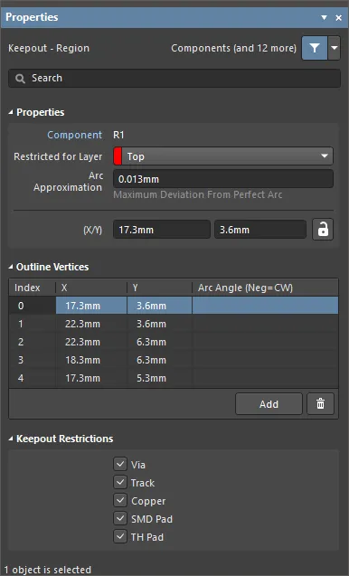
The Keepout - Region mode of the Properties panel.
Properties
- Component – this field is shown in the PCB editor only when the selected Region Keepout is a constituent part of a PCB Component and displays the designator of the parent PCB component. Select the clickable Component link to open the Component mode of the Properties panel for the parent component.
- Restricted for Layer - use the drop-down to select the layer on which the region keepout is located.
- Arc Approximation - enter the maximum deviation from a perfect arc.
- Area - the total area of the placed object.
- Locked (Properties panel only) - enable to lock the region keepout.
Outline Vertices
This region is used to modify the individual vertices of the currently selected region object. You can modify the locations of existing vertices, add new vertices or remove them as required. Arc connections between vertex points can be defined, and support is also provided for exporting vertex information to and importing from a CSV-formatted file.
- Vertices Grid - lists all of the vertex points currently defined for the region in terms of:
- Index - the assigned index of the vertex (non-editable).
- X - the X (horizontal) coordinate for the vertex. Click to edit.
- Y - the Y (vertical) coordinate for the vertex. Click to edit.
- Arc Angle (Neg = CW) - the angle of an arc that is drawn to connect this vertex point to the next. By default, connections are straight-line edges, with this field remaining blank. Click to edit then enter an arc angle as required. Entry of a positive value will result in an arc drawn counterclockwise. To draw a clockwise arc, enter a negative value.
Straight-line edges are used to connect one vertex point to the next. If you would rather have an arc connection, enter a value for the required Arc Angle. Entry is made in the field associated to the source vertex point, with the arc being from this vertex to the subsequent vertex below in the list.
- Add - click to add a new vertex point. The new vertex will be added below the currently focused vertex entry and will initially have the same X,Y coordinates as the focused entry. Click
 to remove the currently selected vertex.
Keepout Restrictions
Use this region to select which object types will be restricted by the Keepout. Deselecting an object type will cause the Keepout to allow transgressions by that type of object (not kept out) by not imposing the applicable Clearance Rule. Choices include:
- Via
- Track
- Copper
- SMD Pad
- TH Pad
Fill Keepout

A Fill Keepout
A fill keepout is a primitive design object that can be placed on any layer. As well as the standard fill that is used for design tasks such as defining a component outline, there is a second type of fill available that is referred to as a fill keepout. A fill keepout can be placed as a layer-specific keepout object or an all-layer keepout to act, for example, as a placement or routing barrier. The difference between a standard fill and a keepout fill is that layer-specific keepout-type fills are not included in output generation, such as Gerber or ODB++. A keepout fill is identified by having an outline in the Keepout color.
A fill keepout can only be placed on a signal layer or the Keepout layer.
After launching the fill keepout placement command, the cursor will change to a cross-hair and you will enter fill keepout placement mode. Placement is made by performing the following sequence of actions:
- Click or press Enter to anchor the first corner of the fill keepout.
- Move the cursor to adjust the size of the fill keepout then click or press Enter to anchor the diagonally-opposite corner and complete placement of the fill keepout.
- Continue placing further fill keepouts or right-click or press Esc to exit placement mode.
The graphical method of editing allows you to select a placed object directly in the design space and graphically change its size, shape or location.
When a fill keepout object is selected, the following editing handles are available:
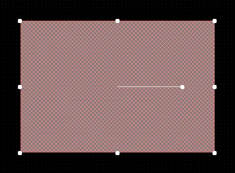
A selected Fill Keepout
- Click, hold and drag the corner handles to resize the fill keepout in the vertical and horizontal directions simultaneously.
- Click, hold and drag the side, top and bottom handles to resize the fill keepout in the vertical and horizontal directions separately.
- Click, hold and drag the middle handle to rotate the fill keepout about its center point.
- Click anywhere on the fill keepout away from editing handles then hold and drag to reposition it. While dragging, the fill keepout can be rotated or mirrored:
- Press the Spacebar to rotate the fill keepout counterclockwise or Shift+Spacebar for clockwise rotation. Rotation is in accordance with the value for the Rotation Step defined on the PCB Editor – General page of the Preferences dialog.
- Press the X or Y keys to mirror the fill keepout along the X-axis or Y-axis.
Fill Keepout Properties

The Keepout - Fill mode of the Properties panel.
Location
- (X/Y)
- X (first field) - the current X (horizontal) coordinate of the reference point of the fill keepout, relative to the current design space origin. Edit to change the X position of the fill keepout. The value can be entered in either metric or imperial; include the units when entering a value whose units are not the current default.
- Y (second field) - The current Y (vertical) coordinate of the reference point of the fill keepout, relative to the current origin. Edit to change the Y position of the fill keepout. The value can be entered in either metric or imperial; include the units when entering a value whose units are not the current default.
- Rotation - the fill keepout's angle of rotation (in degrees), measured counterclockwise from zero (the 3 o'clock horizontal). Edit to change the rotation of the fill keepout. Minimum angular resolution is 0.001°.
Properties
- Component – this field is shown in the PCB editor only when the selected Fill Keepout is a constituent part of a PCB Component and displays the designator of the parent PCB component. Select the clickable Component link to open the Component mode of the Properties panel for the parent component.
- Restricted for Layer - use the drop-down to select the restricted layer.
- Area - provides the area of the placed object.
- Length - displays the current length of the fill keepout. Edit this field to change the length within the range 0.001mil to 10000mil.
- Width - displays the current width of the fill keepout. Edit this field to change the width within the range 0.001mil to 10000mil.
Values can be defined in either mm or mil units. When entering a value in units other than the current units, add the mm or mil suffix to the value.
Keepout Restrictions
Use this region to select which object types will be restricted by the Keepout. Deselecting an object type will cause the Keepout to allow transgressions by that type of object (not kept out) by not imposing the applicable Clearance Rule. Choices include:
- Via
- Track
- Copper
- SMD Pad
- TH Pad
Placing Keepouts
A Keepout is placed in the editor design space from the Place » Keepout menu, where the nominated Keepout style (Track, Fill, Region, or Arc) will be placed on the currently active Layer. Select the Keepout’s Properties to edit its physical characteristics, layer or object type restrictions. The related Keepout properties are:
- Restricted for Layer – sets the Keepout Layer, and therefore the board layer on which copper objects will be restricted (kept out). For an all-layer keepout, select the Keep-Out Layer.
- Keepout Restrictions – determines which object types will be restricted by the Keepout. Deselecting an object type will cause the Keepout to allow transgressions by that type of object (not kept out), by not imposing the applicable Clearance Rule.
Keepouts can be placed on all (copper) signal layers, excluding copper planes. When the currently active board layer is not compatible with Keepouts, the Place » Keepout command is not available (grayed out).
In the below image, the two Keepout Fills have different Layer and object restrictions applied. These allow the Top Layer Keepout Fill (on the left) to accept a Through Hole (TH) Pad while restricting all other object types, and the Keep-Out Layer (right) to accept tracks only.
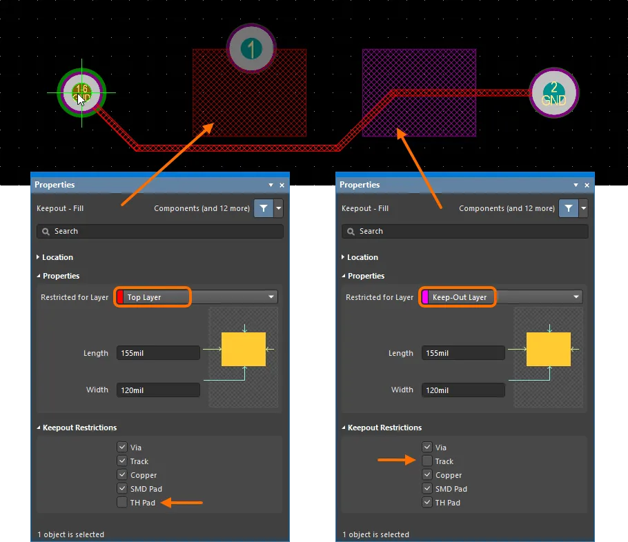
Example of two Keepout Fills placed on different layers of a PCB and configured to restrict placement of different object types.
The inherent flexibility of Keepouts allows their use for a wide range of tasks to control PCB layouts. Since Keepouts can be overlaid, assigned to any signal layer (such as Top or Bottom), and configured to reject specific objects, they can be used to tightly control Via Stitching and Polygon Pours, for example.
Polygon Pour Control
In the example PCB layout shown below, Keepout Fills have been added around the multilayer Pads in a region of potential high voltage, which needs to have sufficient electrical isolation from the pending ground-connected Polygon Pours. The Keepout Fills are set to Top Layer and configured to restrict only Copper objects, which will reject Polygon Pours, Fills and Regions while accepting existing tracks and pads, etc. – in other words, the Clearance violation Rule will only apply to objects classed as 'copper'.
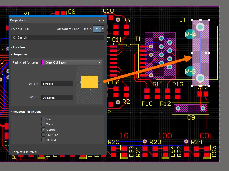
Keepout Fills placed on the Keep-Out Layer and configured to be applied to copper objects only.
The above arrangement of Keepouts will force Polygon Pours placed on the signal layers (in this case the Top and Bottom Layers) to avoid all three Keepout areas. However, the top layer pads associated with the area of concern will not be provided with adequate clearance by the Top Layer Pour.
In this case, further Keepouts can be added to the Top Layer so that its Polygon Pour will avoid all the related pads by a suitable distance. In the image shown below, another two Keepout Fills have been added to the Top Layer, which is displayed here in Single Layer mode for clarity. Note that the Keepout coverage shown could have been created from a single Region, rather than two overlapping Fills.
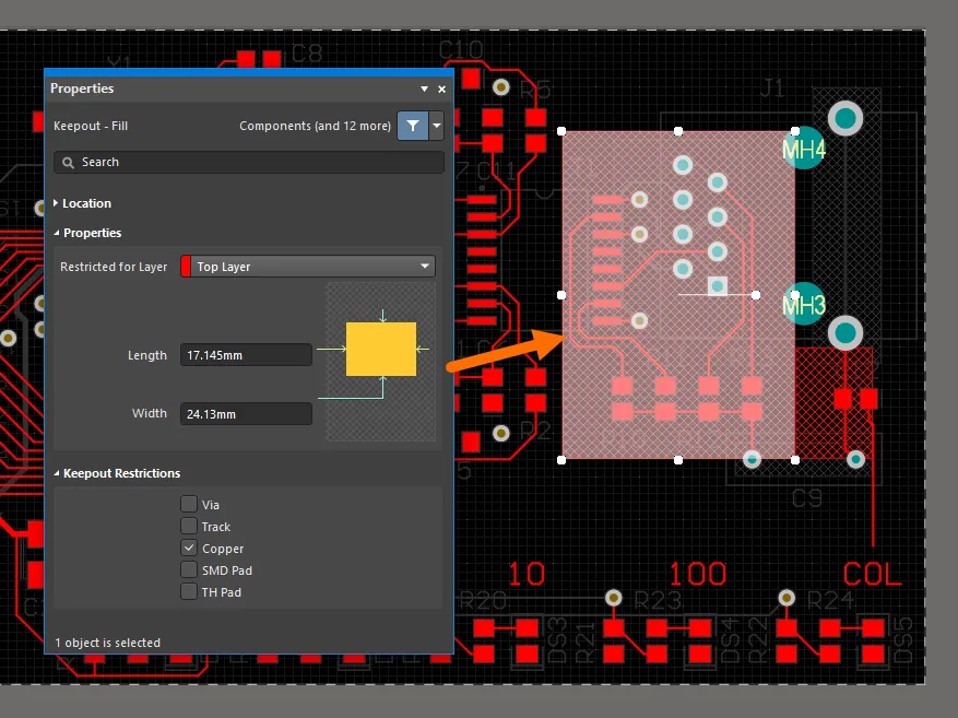
Keepout Fills placed on the Top Layer and configured to be applied to copper objects only.
When the Polygon Pours are eventually added to the layout, the collection of Keepouts will control the pours to produce a different clearance shape for each layer around the region. Note that in this example, the clearance associated with Keepouts is greater than that for normal objects due to a custom Keepout Clearance Rule (see below).
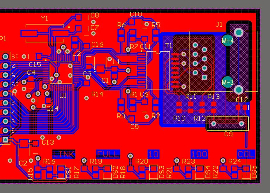
Polygon Pours avoid placed Keepout objects.
The influence of the Keepout collection on the Polygon Pours can be seen clearly when the layout is viewed in Single Layer 3D mode, as shown below – Top Layer on the left and Bottom Layer on the right.

The Top Layer (left) and Bottom Layer (right) of the PCB shown in Single Layer 3D mode.
Note that the approach to controlling Polygon Pour areas is used here as an example for placing and configuring Layer Specific Keepouts. In practice, the area occupied by a Polygon Pour is best controlled by using
Polygon Pour Cutouts.
Via Stitching Control
The application of Keepout shapes, configured to restrict Via objects, on multilayer copper areas can control the extent of automated Via Stitching (Tools » Via Stitching/Shielding). The Keepout shapes can be set for any layer or one of the copper area layers so that Vias between those layers will be ‘kept out’ (restricted).
In the example shown below, Keepout shapes have been added to the upper and lower left corners of the layout. These are configured to restrict Via objects, which will prevent the automated Via Stitching from placing Vias within those perimeters.
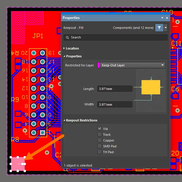
Keepout Regions configured to be applied to vias only.
Along with avoiding existing Tracks, Pads and Vias, as is normally the case, the Via Stitching also avoids the Keepout shapes as determined by the applicable Clearance Rule.
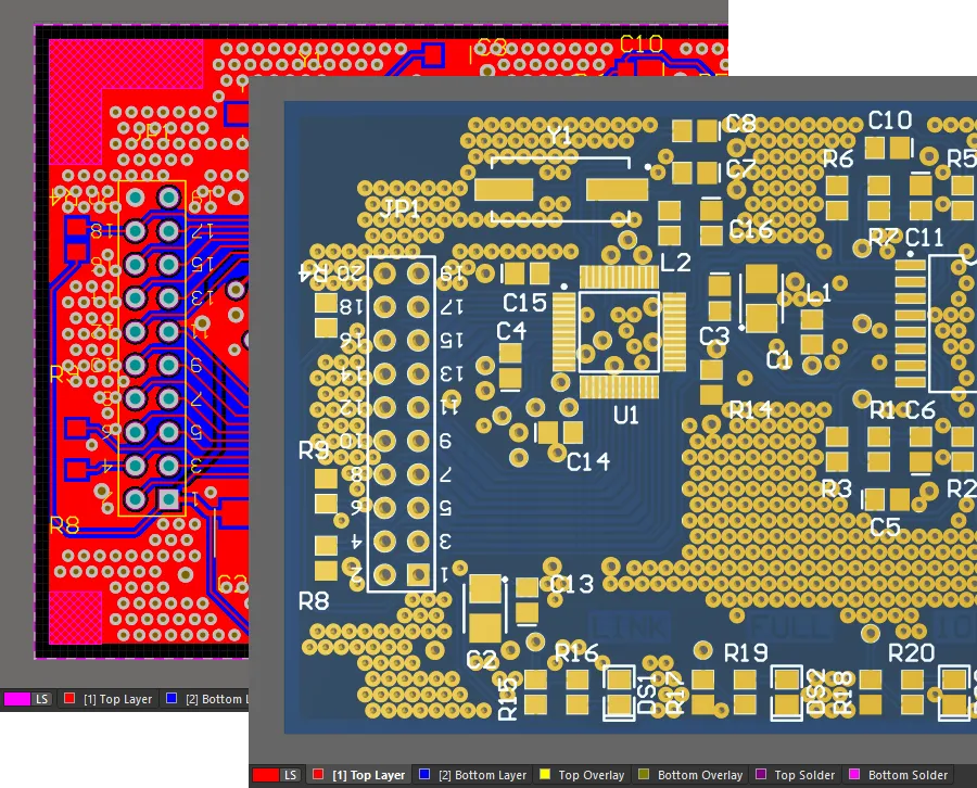
The PCB after adding via stitching.
Keepouts in Components
Keepouts are added to component Footprints in the PCB Library Editor using the same approach as those applied within the PCB Editor design space.
The Keepout added to the component Footprint shown below is configured to restrict all objects, but allow tracks – therefore enabling Net connections in a layout where the component is used, while restricting the close placement of other object types.
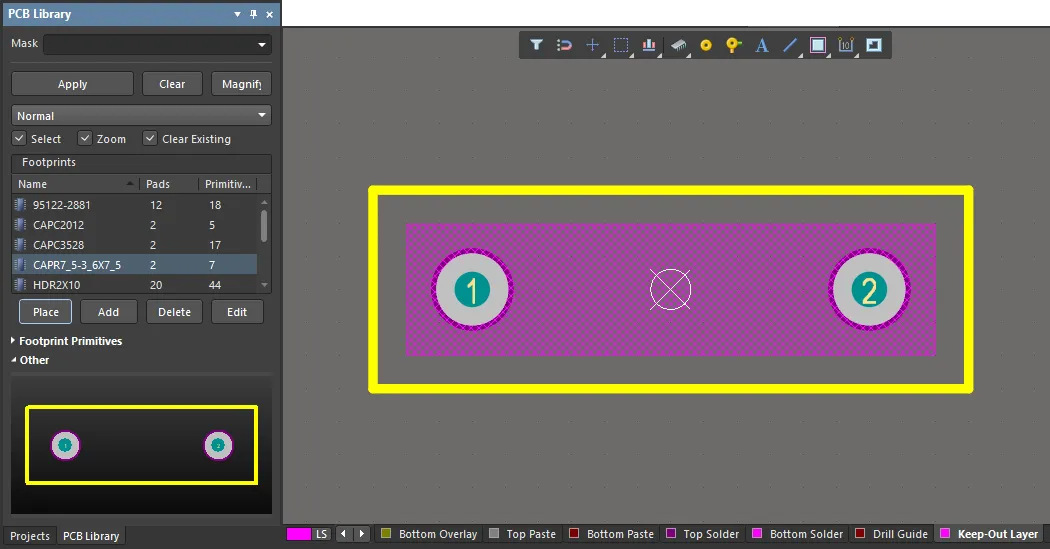
Keepout object can also be added to component footprints, in the PCB Library Editor.
Note that Design Rules are not applied in the PCB Library Editor, so the Keepout, in this case, will accept the Through Hole Pads that are within its bounds.
Working with Keepouts
The implementation of Altium Designer’s Object Specific Keepouts is reflected in all associated functions, and includes compatibility with the Queries (and therefore Design Rules), the PCB List panel, and also imported/older PCB design documents.
Keepout Clearance Rule
As is the case for other object primitives, the current Electrical Clearance Rule will determine the clearance constraints for Keepouts – see Design » Rules. If a different clearance constraint is required for Keepouts, create a specific Rule by applying the IsKeepOut Attribute Check as a Custom Query.
Ensure that the custom Keepout Clearance Rule is set to a higher priority than the existing (global) Clearance Rule. In the example below, a rule has been created for Keepouts (Clearance_Keepout) with double the clearance constraint distance of the base Clearance Rule (Clearance). As shown in the section of board layout, the track routed between the two pads avoids the Keepout region (on the right) by a larger margin than the Top Layer region (left).
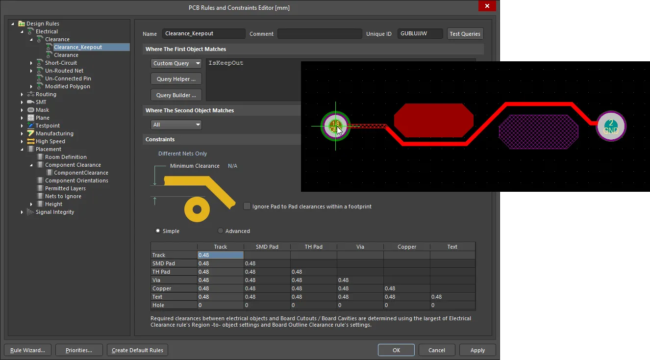
An additional Clearance rule for Keepout objects can be created.
Convert Primitive Objects to Keepouts
Existing primitive objects on signal layers can be converted to Keepouts, on the same layer, using the Convert Primitives to Keepouts command (Tools » Convert » Convert Selected Primitives to Keepout).
Keepout objects can be converted (back) to their equivalent non-Keepout primitive objects using the Tools » Convert » Convert Selected Keepouts to Primitives command.

A primitive object can be converted to an equivalent Keepout object (and vice-versa).
Access via Panels
Object-specific Keepouts in a board design can be accessed via the PCB List and PCB Filter panels.
The PCB Filter panel allows the use of the IsKeepOut query keyword to locate and (optionally) select Keepouts objects in the design.

The PCB Filter panel can be used for locating Keepout objects in the design.
The PCB List panel can be used to list, select and edit the Keepout object of the selected type – for example, Keepout Fills, as shown in the below List panel image. A standard Top Layer Fill (the last listed) is also shown for comparison. If all the Fills (or other types of objects, such as Regions) included in the design are assigned as Keepouts, then the PCB List panel will include the full set of Keepout object Restriction attributes.

The PCB List panel can be used to list, select and edit the Keepout object of the selected type.
Note that the Keepout attribute listed in the PCB List panels is read-only since the Fill, in this case, is designated as a Keepout object. Similarly, the Net attribute for Keepout objects in the PCB List panel cannot be edited because Keepout objects, by definition, cannot be assigned to a Net.
Importing PCB Designs
Altium Designer is able to import design files from a wide range of other design tools using the automated conversion capabilities provided by the Import Wizard (File » Import Wizard). Keepout type objects that are included in PCB design files from other design tools, some of which are object-specific, are converted to Object Specific Keepouts by the Wizard, where possible.
The Wizard’s Keepout conversion process is compatible with board designs from popular ECAD systems such as Mentor® Graphics Pads™ and Cadence® Allegro™. Correct Keepout interpretation also occurs during the IDF export process.