
Working with Classes on a Schematic & PCB
A Class is a named group of objects. As well as helping the designer select objects of interest as they browse the design, classes can also be used to apply design requirements to all objects in that group, or class.
Classes can be generated based on structural aspects of the design, like nets or components on the same sheet, or nets in the same bus. These structural, software-generated classes include: Component, Net, Design Channel and Structure.
User-defined classes can also be created; either through the Constraint Manager if that is your preferred approach to defining design requirements, or using schematic parameters and PCB classes if you prefer a design-rules based approach.

Classes provide an excellent way to manage logical groups of components and nets, here the routing requirements are being applied to the LEDS class in the Constraint Manager.
Supported Classes and Where They Are Defined
Support for class definition was initially introduced in the PCB editor, through the Object Class Explorer. Following this, support was added for defining the most-often used classes in the schematic editor, that is, components and nets. Components can be added to a class by adding the ClassName parameter to the component, and nets by attaching a parameter set directive that includes the Net Class Name parameter. These class definitions are detected and transferred to the PCB during design synchronization.
The introduction of the Constraint Manager bought a simpler and more structured approach to defining requirements such as classes, along with the other physical and electrical requirements of the design. Constraints are project-level settings which can be edited at any time from either the schematic editor or the PCB editor, but still must be synchronized through the ECO system.
In the situation where there are both parametric net class definitions and Constraint Manager net classes present, the parametric definitions are not applied. The table in the collapsible section below details all supported class types, and where they can be defined.
Available Class Types
| Class Type | Software-created based on structure |
Schematic Editor parameters |
PCB Editor Object Class Explorer |
|
| Net | ✓ |
🗸 |
✓ | ✓ |
| Component | ✓ |
🗸 |
✗ | ✓ |
| Layer | ✗ | ✗ | ✗ | ✓ |
| Pad | ✗ | ✗ | ✗ | ✓ |
| From-to | ✗ | ✗ | ✗ | ✓ |
| Differential Pair | ✗ | ✗ |
✓ | ✓ |
| xNet | ✗ | ✗ | ✓ | ✗ |
| xSignal | ✗ | ✗ | ✓ | ✓ |
| Design Channel | ✓ |
✗ | ✗ | ✓ |
| Polygon | ✗ | ✗ | ✗ | ✓ |
| Structure | ✓ |
✗ | ✗ | ✓ |
Defining Classes with Schematic Parameters
You can create user-defined component classes and net classes by adding or attaching a parameter to the relevant component or net. PCB component and net classes will then be created if the appropriate User-Defined Classes checkboxes are enabled in the Class Generation tab of the Options for Project dialog. Read more about configuring these options.
User-Defined Component Class
To add components to a component class, add a parameter to the component with the parameter Name string set to ClassName, and the parameter Value string set to the name of the class. The parameter must be added to every component that you want included in the class. This can be done in a single editing action by selecting all of the components first and then adding the parameter in the Properties panel. Alternatively, if the components are located together, a Blanket directive can be used, with a Parameter Set directive attached.
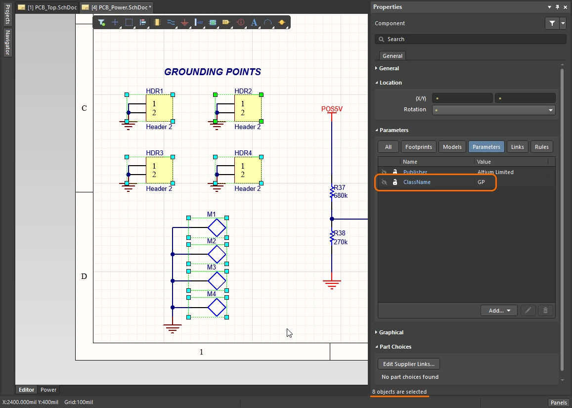
![]()
User-Defined Net Class
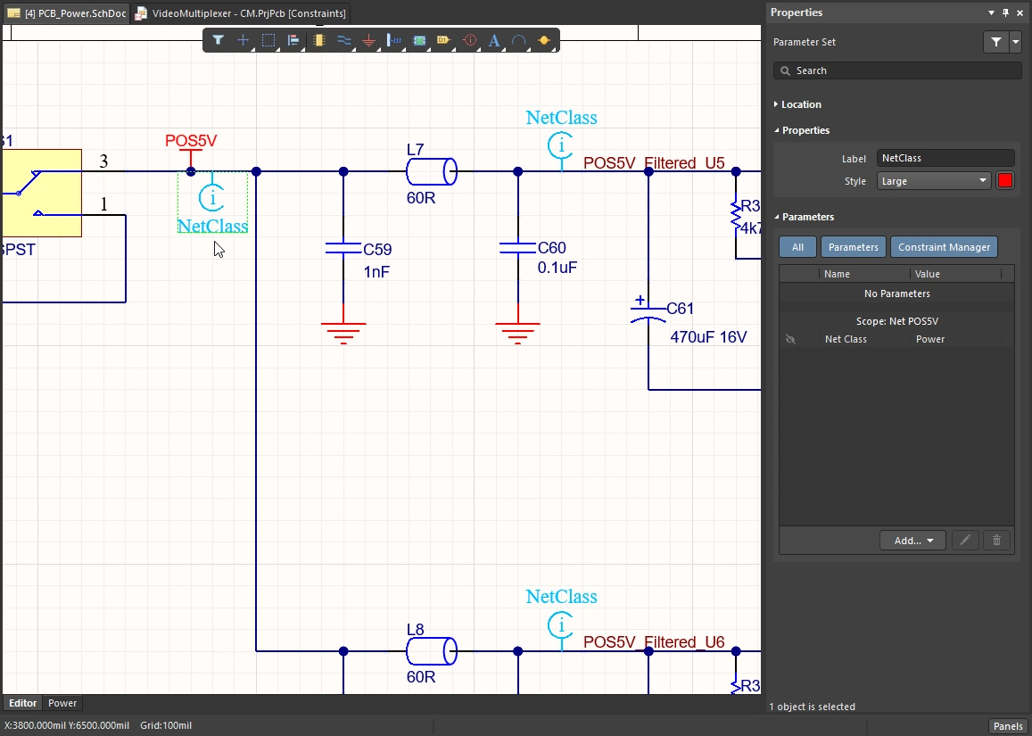
To parametrically add a net (or the nets in a bus or signal harness) to a PCB net class, you attach a parameter to that net / bus / harness. You can attach parameters to a net by placing a Parameter Set directive with its end touching the net / bus / harness, and then adding the Net Class Name parameter to that directive.
This Parameter Set directive can be copied and pasted to different locations on the schematic to add multiple individual nets to the same PCB net class. Alternatively, a Blanket directive can be used.
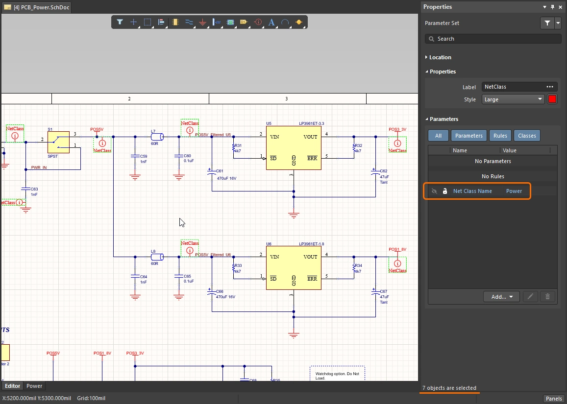
![]()
Using a Blanket to Apply a Directive to Multiple Nets
You can also add multiple nets to a PCB net class by placing a Blanket directive that covers all of those nets. The function of a Blanket is to allow you to apply a directive to all of the nets under the blanket (either identified by a net identifier, such as a Net Label or Power Port that is under the blanket, or a net that has at least one end vertex contained within the Blanket).
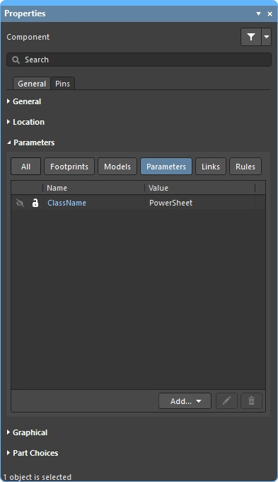
Instead of placing the Parameter Set directive so that it touches a wire, you place it so that it touches the edge of the blanket, as shown in the image below. Note that it is the value of the Parameter within the Parameter Set object that defines the PCB net class name, not the display name of the Parameter Set object. In the example image below, the Parameter Set is also used to define a routing width design rule.

Using a Blanket directive to bundle all the nets under it, into a PCB net class called Power. Note that the name of the Parameter Set directive is not used for naming the class, it is a visual reference only.
Defining Classes in the Project Constraint Manager
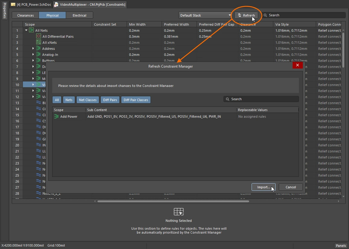
Classes are a key feature of working with the Constraint Manager, making it easy to apply and adjust design constraints across multiple nets. In the Constraint Manager, classes are added, edited and deleted using commands in the context-sensitive right-click menu, as demonstrated in the video below. Nets can be added individually, or multi-selected using the standard Windows techniques, before being added to a class.
The Constraint Manager Object Class Explorer can be used to examine and edit all classes across the project. All of the classes defined in the Constraint Manager are transferred to the PCB during design synchronization, regardless of the configuration of the options in the Class Generation tab of the Options for Project dialog.
A simple demonstration of creating a class of nets in the Constraint Manager.
Learn more about the Constraint Manager.
Classes Generated During Design Transfer
The creation of automatically generated classes, as well as classes derived from schematic parameters, are configured in the Class Generation tab of the Options for Project dialog.
-
Automatically generated classes - derived from the project structure, can include buses/harness (net classes), sheet contents (component classes), and project structure (structure classes). These classes are generated when the design is transferred from schematic to PCB, and are available regardless of the approach chosen to manage the design constraints (Constraint Manager, or Design Rules). They are not available in the schematic editor during design capture – for example, browsing in the Navigator panel.
-
User-defined classes - derived from design parameters added to the component or net. Note that classes defined in the Constraint Manager are not managed by these options.
The generation of these classes is configured in the Class Generation tab of the Options for Project dialog. Note that what classes are ultimately synchronized to the PCB is controlled by options in the Comparator tab, ensure these are configured as required.

Use the options in the Class Generation tab to configure the generation of derived classes and user-defined classes during design synchronization.
Automatically Generated Classes
| Generate Net Classes for Buses | Automatically generate a net class for each named bus in the design. The members of the class will be the nets in that bus. |
| Generate Net Classes for Components | Automatically generate a net class for each component in the design. The members of the class will be the nets connected to the pins of that component. The net class will be named using the designator of the component, in the format <ComponentDesignator>_Nets. |
| Generate Separate Net Classes for Bus Sections | Automatically generate a separate net class for each bus section. A bus section is created by specifying a bus that is actually a section of a larger bus, for example, A[2..0] from the bus A[15..0]. |
| Generate Net Classes for Named Signal Harnesses | Automatically generate a net class for each named signal harness in the design. The members of the class will be the nets associated with the signals gathered by the named signal harness. A named signal harness has a net label attached to it; the generated net class is given this name. |
| Schematic Sheet | The grid section of the dialog lists all sheets in the project. For each sheet, you can selectively generate: a component class, a PCB room, a net class and a structure class. |
| Sheet Name/Full Path | Name and location of the schematic sheet. |
| Component Classes | Column of checkboxes. If enabled, a component class, containing all components on that sheet, is created (named the same as the sheet symbol name). |
| Generate Rooms | Column of checkboxes. If enabled, a room is created automatically for that schematic sheet (only available If the Component Class checkbox is enabled). The PCB room has the related component class assigned to it. Rooms are placed at the bottom left of the PCB during initial design synchronization. Learn more about Working with Rooms. |
| Net Classes Scope | Use these options to determine if a class of the nets within this schematic sheet is generated (the class is named the same as the sheet symbol name).
|
| Structure Classes | Enable to generate a structure class. The members of the structure class include the enabled component class and net class. Edit the Structure Class in the PCB editor to add other net / component / structure classes. Use the Structure mode of the PCB panel to locate the components and nets in that structure class. |
User-Defined Classes
| Generate Component Classes | Enable to generate user-defined component classes. To add a component to a user-defined component class, add the |
| Generate Rooms for Component Classes | Enable this option to generate a PCB placement room for each generated user-defined component class, and assign that component class to the room. The placement room has the same name as the component class. |
| Generate Net Classes | Enable this to generate user-defined net classes. Parameters are added to a net by attaching a parameter set object to the net, and then adding a If the project uses the Constraint Manager, net classes are not created from parameter set objects. |
 ).
). ).
). ).
). ).
). ).
).Creating Classes in the PCB Editor
Altium Designer's PCB editor started life as a design-rules centric editor, with the PCB requirements being defined in the PCB Rules and Constraint Editor dialog (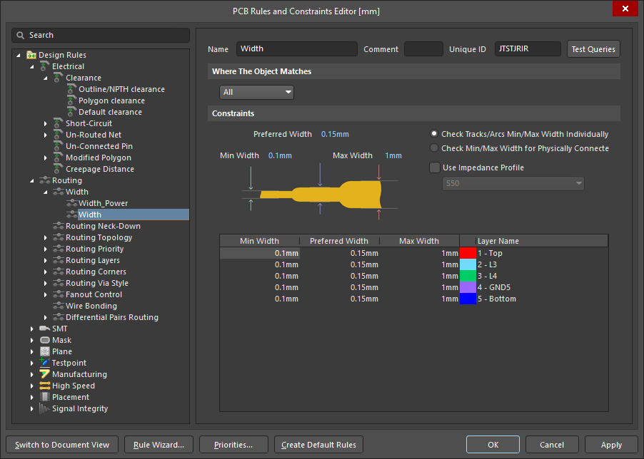 ), and design classes being defined in the PCB editor Object Class Explorer (
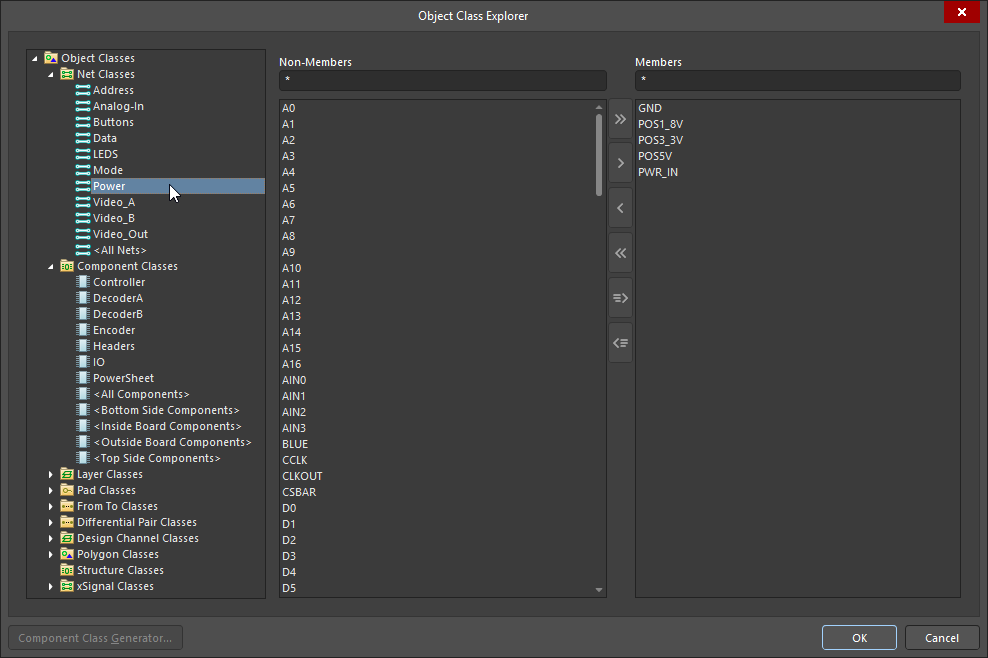 ). This is the default approach used in a new project.
If the Constraint Management option is enabled during project creation, then the requirements are configured in the Constraint Manager () instead of the PCB Rules and Constraint Editor dialog. In this situation, the full range of classes can still be defined and edited in the PCB editor Object Class Explorer, with the sub-set of class-types that can be passed back and forth between the schematic and the PCB also being editable in the Constraint Manager's Object Class Explorer (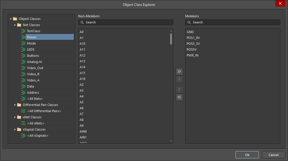 ).
).
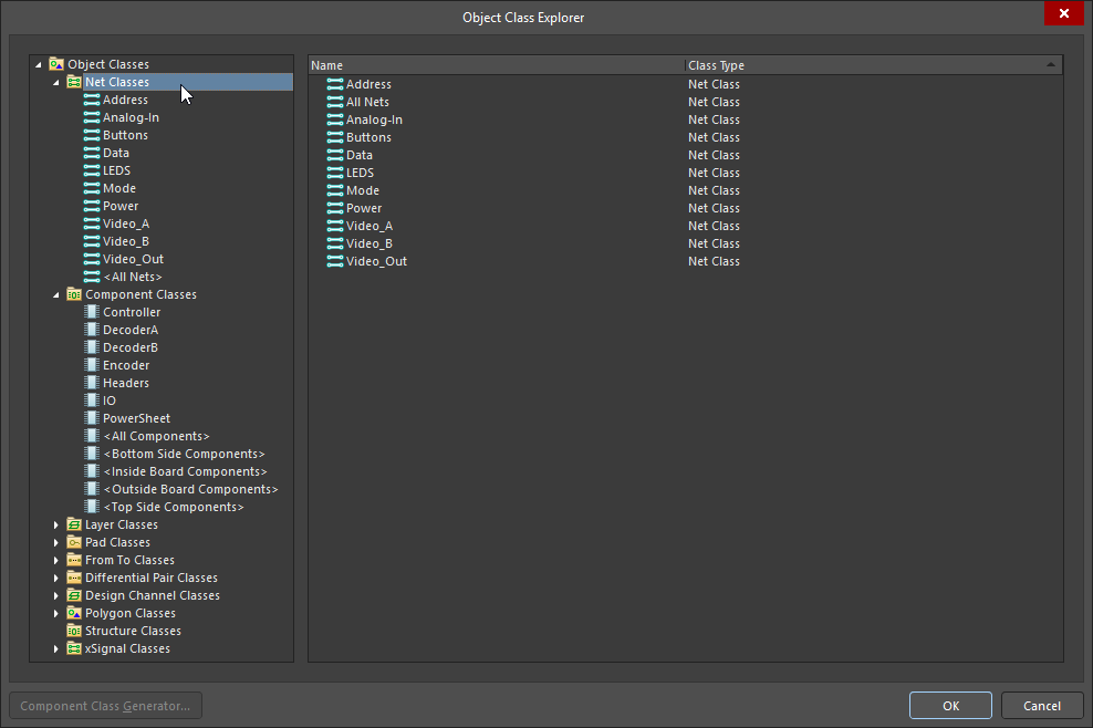
PCB Object Class Explorer
Classes can be added, edited and removed in the Object Class Explorer.
-
To access and edit the full range of classes available in the PCB editor, select Design » Classes from the PCB editor menus to open the Object Class Explorer.
-
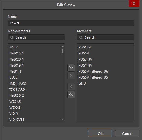
The Constraint Manager Object Class Explorer can also be used to edit the classes that are synchronizable between the schematic and PCB. To access it, right-click in the Constraint Manager and select Classes » Class Explorer from the context menu.
Object Class Explorer (PCB editor)
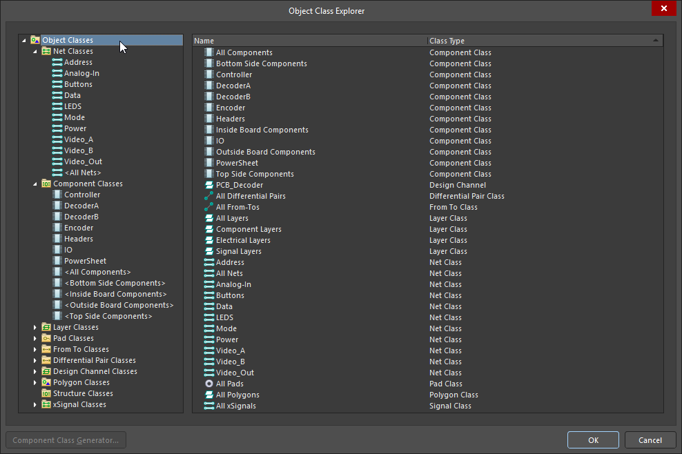
| Class Types and Classes | The tree structure in the left panel of the dialog is used to browse all of the object classes available in the PCB. Click on the Object Classes icon at the top of the tree to display a list of all classes currently defined in the design ( |
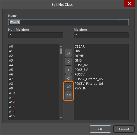
| Non-Members | When a specific class is selected in the tree on the left of the dialog, the center column displays a list of all objects that are not currently members of the selected class. Select non-members to be added to the current class (using standard Windows selection techniques), then use the controls between the Non-Member and Member panels to add the selected members to that class (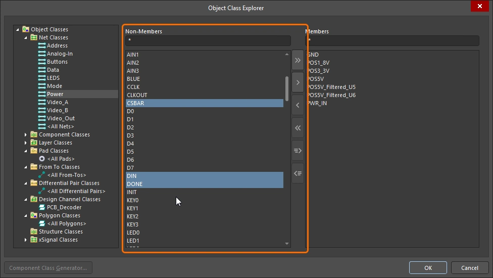 ). ). |
| Members | When a specific class is selected in the tree on the left of the dialog, the right-hand column displays a list of all objects that are currently members of the selected class. Select members currently in the class (using standard Windows selection techniques), then use the controls between the Non-Member and Member panels to remove the selected members from that class (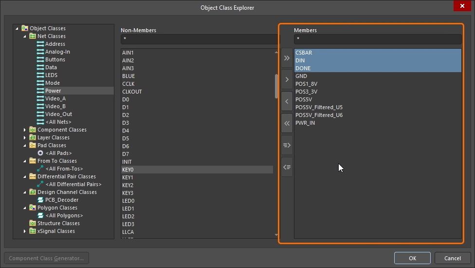 ). ). |
| |
Add all Non-Members to the Members list. |
| |
Add currently selected Non-Members to the Members list. |
| |
Remove currently selected Members from the list. |
| |
Remove all Members from the list. |
| |
Add objects that are currently selected in the design space, to the Members list. This control is only available when it is possible to pre-select the object(s) in the design space. |
| |
Remove objects that are currently selected in the design space, from the list. This control is only available when it is possible to pre-select the object(s) in the design space. |
| |
The Component Class Generator button is only available when creating/editing a component class. Clicking on it opens the Component Class Generator dialog, which can be used to quickly generate the membership for the component class, based on the defined search criteria. |
 )
) )
) )
) )
)Selecting Across Editors
A key feature for working between the various editors is the Cross Select Mode, where each component or net that you select on one editor, is also selected in the other editors. Cross Select Mode is enabled via the Tools menu in any editor that supports it (or be pressing the Shift+Ctrl+X shortcut keys). When you click on a component or a net object in one editor, that object is automatically selected in other open editors.
To work across the logical connections in the schematic (nets connected by net labels, ports, and so on), hold Alt as you click to select on a net in the schematic editor. This will select the entire net/bus/harness on each sheet in the project, zooming to show the chosen net objects. How the results present visually on the target pages is controlled by the Cross Select Mode and Highlight Methods options on the System – Navigation page of the Preferences dialog (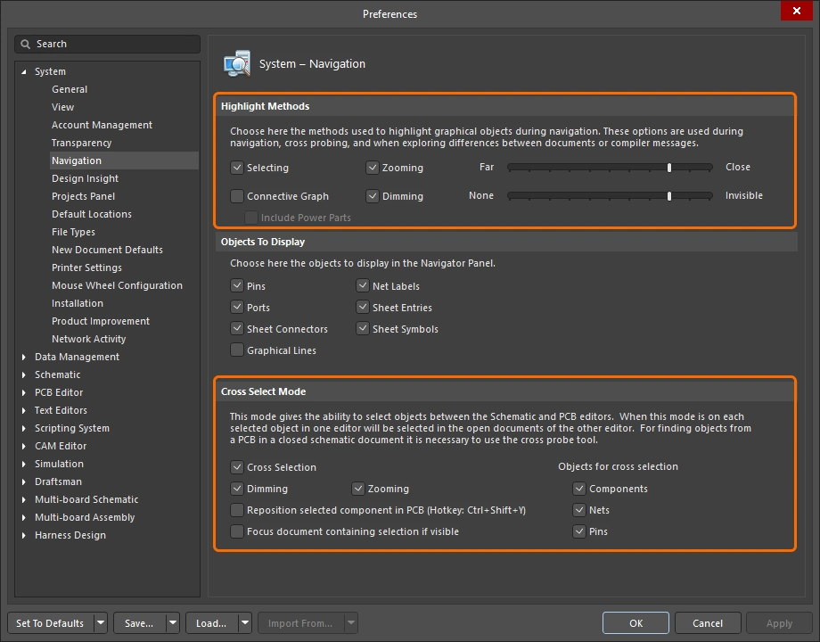 ).
).
Enable Cross Select mode to browse between editors.
Working with Classes in the PCB Editor
Classes are logical groups defined by the designer, and as such, provide an excellent aid in helping them structure, analyze and review the design.
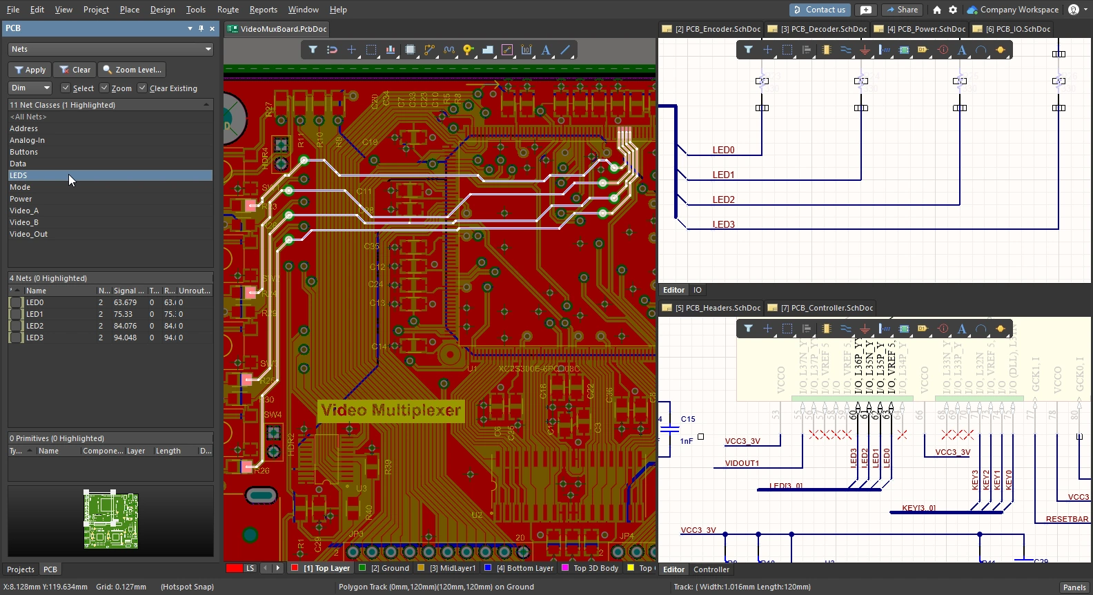
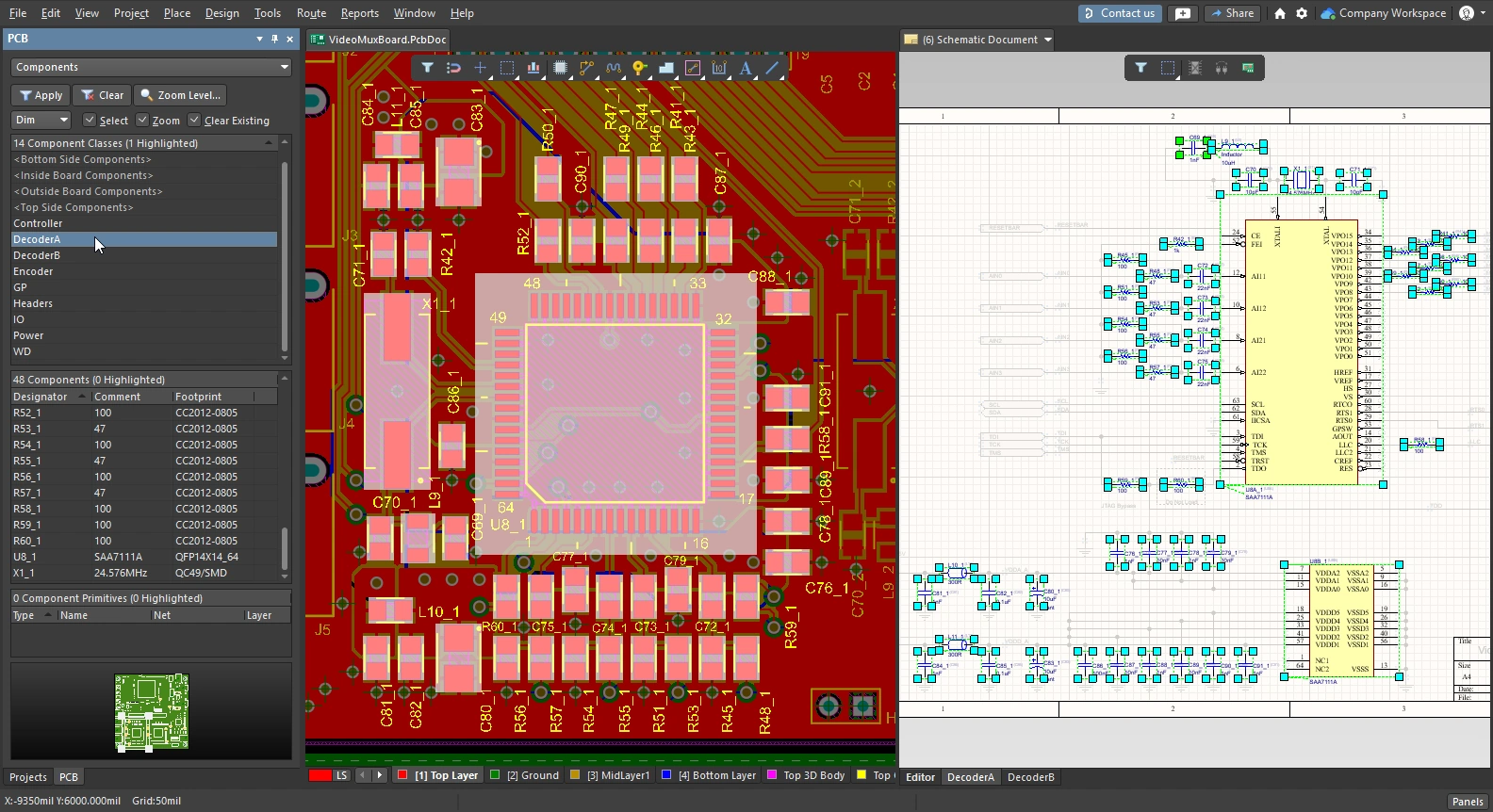
Browsing Classes
The PCB panel supports browsing the PCB in a broad variety of modes, such as by Nets or Components, and for those that support it, you can also browse by classes of those objects. The modes that support browsing by class, include: components, nets, differential pairs, xSignals, polygons, as well as structure classes.
Once the browsing mode has been selected at the top of the panel the top section of the panel will list all of the available classes, as shown in the examples below. If cross-select mode is enabled, then those objects will also be selected on the schematic sheets, when applicable.
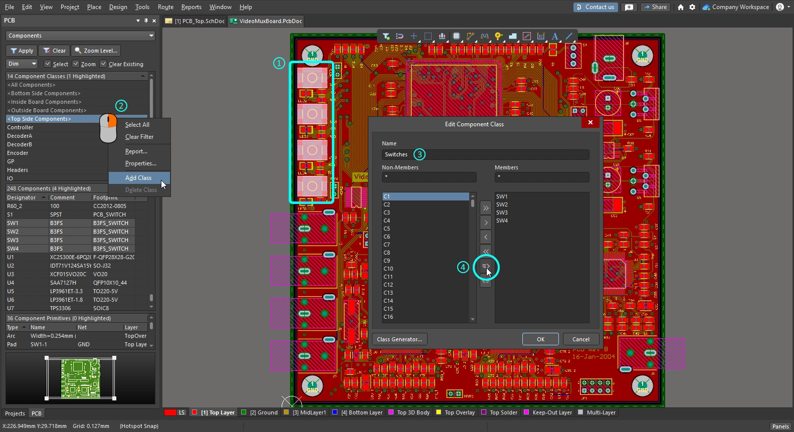
Creating a Class from Selected Objects
You can create a class of a set of currently selected objects in the PCB editor, including: nets, components and polygons.
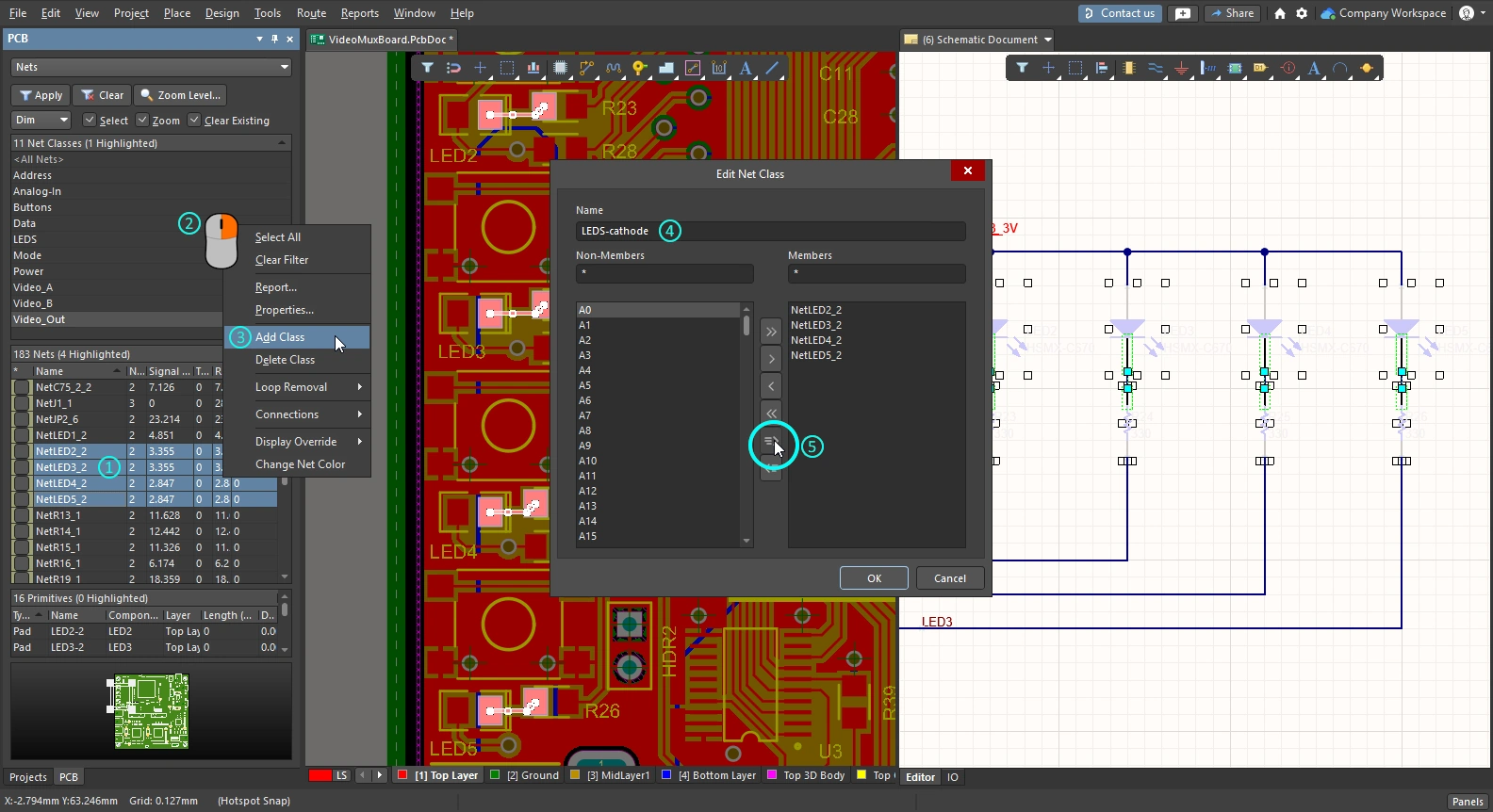
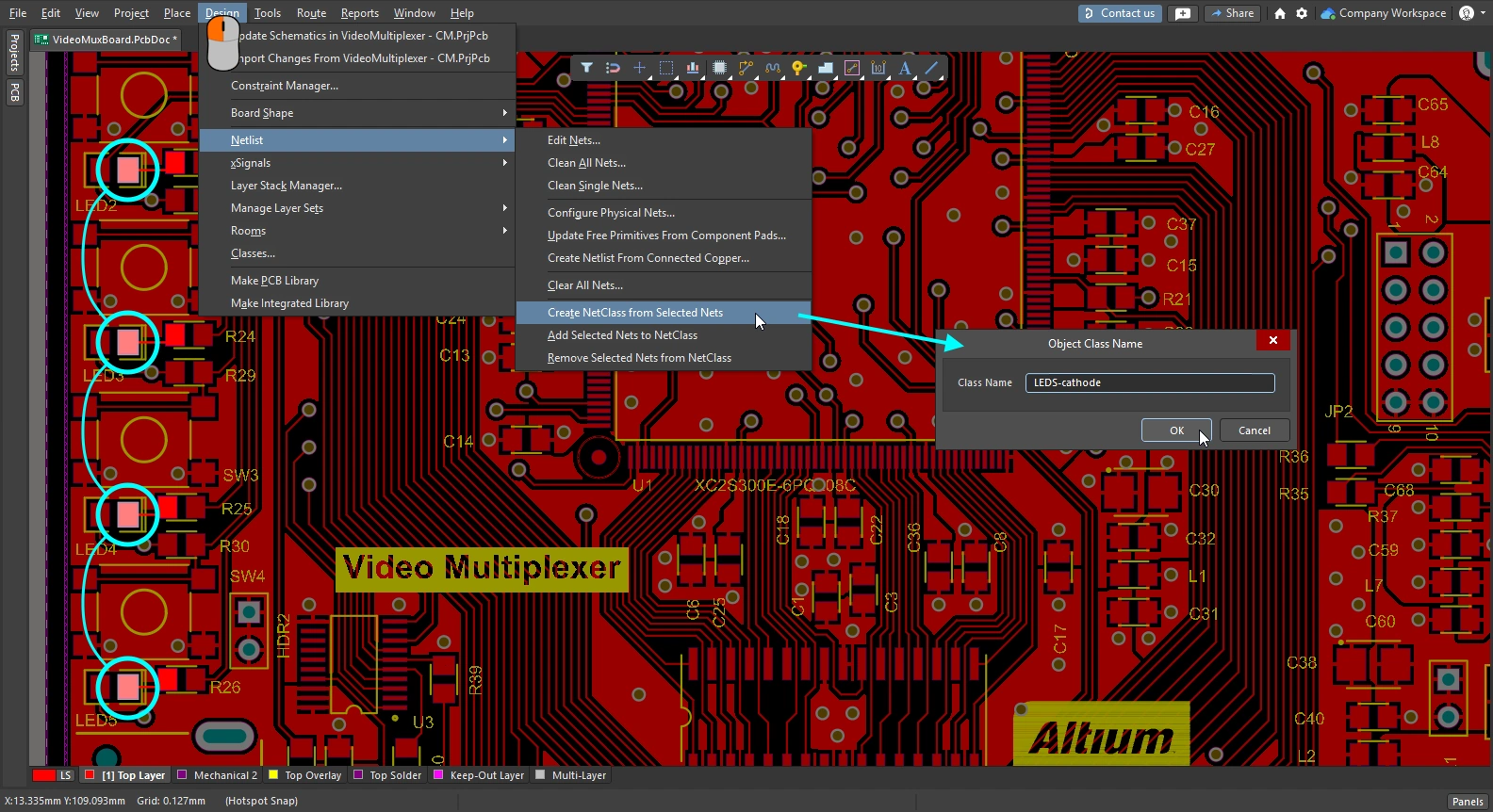
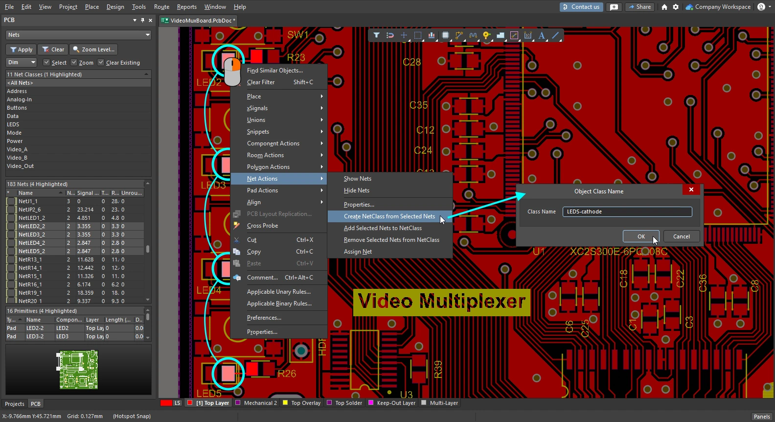
| Net class | Select at least one object in each net in the design space, or select the nets in the PCB panel. Then run the Create NetClass from Selected Nets command from the Design » Netlist sub-menu of the main menus ( |
| Component class | Select the components in the design space or in the PCB panel. Then right-click in the Classes region of the panel to access the Add Class command, as shown in the slides above. Alternatively, select the Design » Classes command to open the Object Class Explorer, where the new class can be created and the selected components added. |
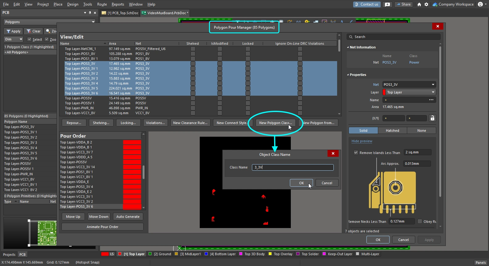
| Polygon class | Select the required polygon entries in the Polygon Manager dialog, then click the New Polygon Class button. Name the new polygon class in the Object Class Name dialog. |
 )
) ).
).Component Class Generator
Another way to create a class of components is using the Component Class Generator. The button to run the generator is available in the PCB Object Class Explorer and the Edit Component Class dialog.
Run the Design » Classes command to open the PCB Object Class Explorer , right-click on the Component Classes list on the left and select the New Class command. Select the new class in the list, then click the Component Class Generator button to open the Component Class Generator. Alternatively, right-click in the Classes region of the PCB panel (Components mode) and select Add Class. Name the new class in the Edit Component Class dialog and then click the Class Generator button to open the Component Class Generator.
 Use the Component Class Generator to quickly build a list of components to include in a class.
Component Class Generator Dialog
| Search/Filter Criteria | The fields on the left of the dialog collectively define the search/filter criteria used to target the components to be added as members of the component class. The Designator, Comment and Footprint fields include a pre-populated list, or you can type in an entry (wildcards are supported). The other fields include a list of available options, select Any to exclude a field from the selection process. |
| Add Matching | Click to add all components that match the defined search/filter criteria to the Class Membership region. |
| Clear Selected | Click to remove all components that are currently selected in the Class Membership region, from the class. |
| Class Name | The field in the upper right area of the dialog presents the current name of the class. Edit this field as required. |
| Class Membership | The region below the Class Name is the Class Membership, listing all components, by designator, that are selected to become members of the component class. Components in the Class Membership list can be selected using standard multi-select techniques: Ctrl+click, Shift+click, and Click+drag. |
Working with Structure Classes
Altium Designer supports the automatic generation of net and component classes when transferring the design from Schematic to PCB. Above this, it also includes the ability to define a hierarchical structure of classes. Essentially, this enables you to group together, at the sheet-level, classes of components and/or nets, into a parent class generated from that sheet. This class can be a child of the parent class above, all the way up to the top-level sheet in your design.
Each of these generated parent classes is referred to as a Structure Class. Structure classes reproduce the schematic document structure within the PCB domain, which is ideal for advanced navigation. They can also be used in logical queries, for example when scoping design rules, or filtering objects in the PCB design space.
Structure Class Concept
A structure class is a special type of class that can hold, as its members, any type of class, including: net classes, component classes, layer classes, pad classes, from to classes, differential pair classes, design channel classes, polygon classes, and other structure classes. By automatically generating a structure class from each schematic sheet in the project – containing components and/or nets – when transferring the design to the PCB, the structure of the project can be faithfully represented on the PCB side.
 The project hierarchy can be represented using structure classes, each class represents a single schematic sheet, with generated sub-classes of member components and/or nets.
The structure classes reflect the hierarchical design created by the schematic sheets. In terms of component and net classes within each structure class, the membership depends on the options specified when generating Component and Net Classes from the source schematic sheets.
Automatic Generation of Structure Classes
The automatic generation of structure classes from the project schematic sheets is configured in the Class Generation tab of the Options for Project dialog (Project » Project Options). To generate a structure class from a source schematic sheet in the project, enable its associated Generate checkbox in the Structure Classes column. If the Component Class checkbox and Net Class Scope options for that schematic sheet are also enabled, they will become the members of that structure class.

Specify which schematic sheets to generate a structure class from, and if that sheets components and nets are to be included.
 )
) )
)Manual Definition of Structure Classes
As with other types of class in a PCB document, you can create and manage structure classes in a manual fashion in the PCB editor. This can be done from the PCB panel, while browsing the class structure hierarchy, or from the Object Class Explorer dialog (Design » Classes). In the dialog, structure classes are defined under the Structure Classes folder, with familiar commands in the right-click menu to add, rename or delete classes as required. Structure classes can include any of the class types supported for use in the PCB design.

Create and manage your Structure Classes as you would any other type of class in the PCB editor, in the Object Class Explorer dialog.
Browsing the Class Structure Hierarchy
In the PCB panel’s Structure Classes mode, the three main regions include:
-
A list of all Structure Classes currently defined for the PCB document; those auto-generated from the schematic sheets as well as those defined in the PCB itself.
-
All Classes that are defined members of the selected structure class.
-
Individual Class Members within the selected class (components, nets, etc.).

Set the PCB panel's mode to Structure Classes to browse the overall class hierarchy for the PCB document.
Structure Classes mode |
|
| Structure Classes region | The top region of the panel lists all structure classes currently defined for the PCB document. These include those automatically generated from the PCB project's source schematic documents (denoted by the |
| Classes region | The middle region of the panel lists all of the class members for the structure class(es) currently selected in the region above. Single-click to zoom and filter the display, double-click to edit a member class. |
| Class Members | The bottom region of the panel lists all members of the class(es) currently selected in the region above. Single-click to zoom to a member, double-click to edit the properties of that member. |
Using Structure Classes in Logical Queries
Logical queries are the fundamental approach used to targeting objects in a PCB design. They can be used when scoping design rules to constrain the design in a specific way, or when filtering objects in the design space. The Query Language supports the use of the Structure Class when building logical query expressions. The following keyword is available in the PCB Functions – Membership Checks section:
InStructureClass – checks whether the object class is in the specified Structure Class.

An example clearance rule between member objects contained within different Structure Classes.
This keyword can also be used when creating a logical query to be used in a filter expression – to quickly filter all low-level member objects descending from the specified Structure Class.

Quickly filtering all objects belonging to a particular Structure Class within the design space.