Adding Via Stitching & Via Shielding
Via stitching is a technique used to tie together larger copper areas on different layers, in effect creating a strong vertical connection through the board structure, helping maintain a low impedance and short return loops. Via stitching can also be used to tie areas of copper that might otherwise be isolated, back to their net.
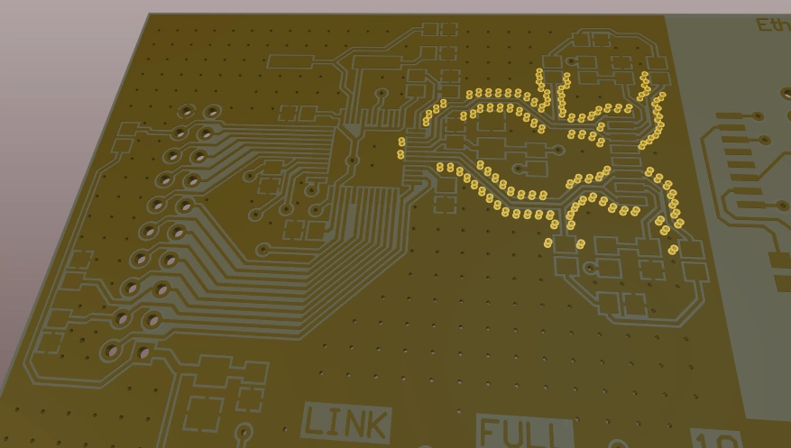
Via shielding has a different function, in RF designs it is used to help reduce crosstalk and electromagnetic interference in a route that is carrying an RF signal. A via shield, also known as a via fence or a picket fence, is created by placing one or more rows of vias alongside the signal's route path. In Altium Designer, this is referred to as via shielding.
Altium Designer supports both via stitching and via shielding. Since the process of adding stitching or shielding vias is similar, this page covers both topics.
Adding Stitching Vias
Via stitching is run as a post-process, filling free areas of copper with stitching vias. For via stitching to be possible, there must be overlapping regions of copper that are attached to the specified net, on different layers. Supported regions of copper include: Fills, Solid Regions, Polygons and Power Planes.
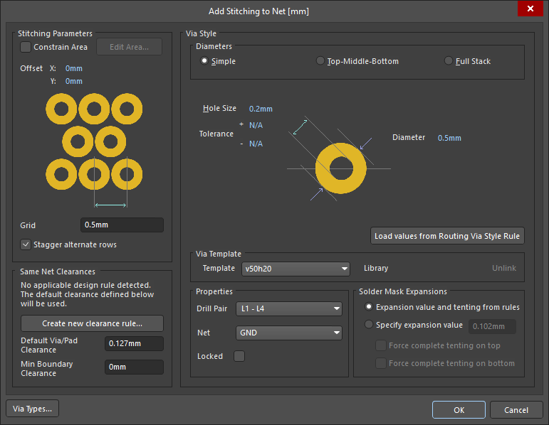
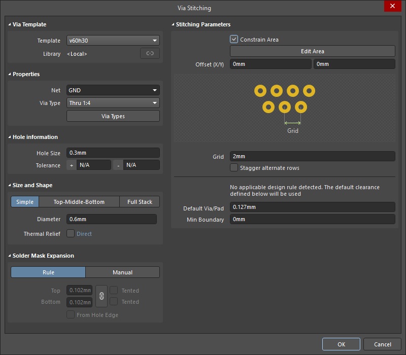
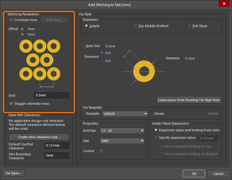
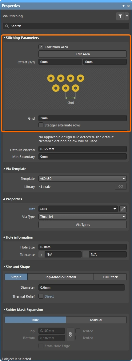
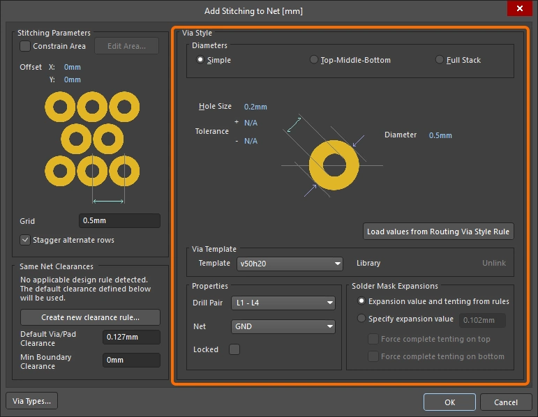
To add stitching vias to a net, select the Tools » Via Stitching/Shielding » Add Stitching to Net command from the menus. The Add Stitching to Net dialog will open, where the Net, Stitching Parameters and Via Style are specified. When the OK button is clicked the stitching algorithm identifies all fills, solid regions, polygons and power planes attached to the selected net and attempts to connect them through the board, using the specified via and stitching pattern.
 )
)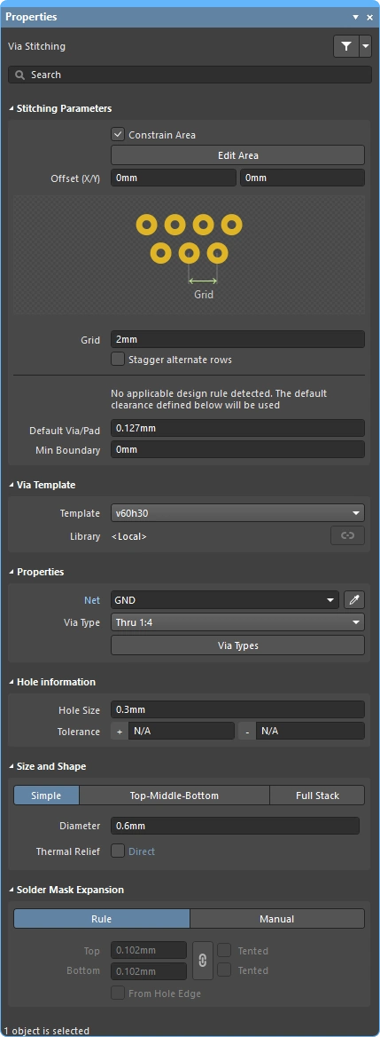 ).
).Stitching Parameters
The Stitching Parameters control where the stitching vias are placed.
Stitching Parameters ( |
|
| Constrain Area | If enabled, via stitching is constrained to a user-defined area of the board. As soon as the option is enabled you are taken to the design space to define the area. When area definition is complete and you right-click, you will return to the dialog to finish the configuration of the stitching vias. The area is defined in the same way as other polygonal objects are placed in the PCB editor, placing edges to define the boundary of the stitching region. Learn more about the process of defining a region on the board. |
| Edit Area | This button is only used when you need to redefine the area where stitching vias have been constrained to, but you have not yet completed the initial stitching process and closing of the dialog. Existing stitching areas can be interactively edited, refer to the Modifying the Via Stitching Area section of this page to learn more. |
| Offset | X and Y offset distance of the first stitching via from the bottom left corner of the board / Constrain Area. |
| Grid | The distance between the center of adjacent stitching vias. The minimum grid value is the diameter of the stitching via. Stitching vias will not be placed in violation of applicable design rules; if a potential via site would result in a violation, that site is skipped. |
| Stagger alternate rows | Alternate rows of shielding vias are offset by half of the Grid value. |
 )
)Same Net Clearances
There are two ways of controlling the clearance between the stitching vias and other vias and pads on the same net: either the applicable Clearance design rule is used, or the Default Via/Pad Clearance specified here is used. If an applicable rule is detected, the rule settings are compared to the Add Stitching to Net dialog settings and the tighter of these are used.
Same Net Clearances ( |
|
| Create new clearance rule (Add Stitching to Net dlg) |
Click to create a new Clearance design rule, configured to define the clearance between the stitching vias, and other vias and pads on the same net. This rule setting is used to ensure a potential stitching site is valid. When the button is clicked, the Edit PCB Rule - Clearance Rule dialog opens, where the rule constraints are set. Note that the rule is named and scoped to target the net selected in the Add Stitching to Net dialog. |
| Edit clearance rule (Add Stitching to Net dlg) |
If an applicable clearance design rule already exists, this button presents instead of the Create new clearance rule button. Click to change the rule settings. |
| Default Via/Pad Clearance | Stitching vias are only placed on potential stitching sites if this much clearance exists. Since potential stitching sites are determined by the stitching grid, it is likely they will be further than apart than this setting. |
| Min Boundary Clearance | Stitching vias are only placed on potential stitching sites if this much clearance exists to the edge of Polygon/Fill/Plane regions. |
Via Style
The properties of the stitching vias are displayed in the Via Style region of the dialog. These properties can be defined by:
-
New settings that you enter into the dialog, or
-
Based on the settings of a selected Via Template, or
-
Based on the settings defined in the applicable Routing Via Style design rule, if you are placing a new set of stitching vias.
Via Style ( |
|
| Diameters (Simple/TMB/Full) |
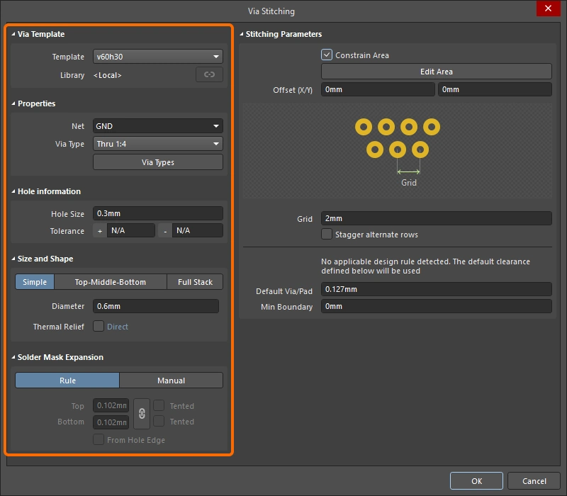
The PCB editor supports 3 types of X-Y plane via diameters: Simple, Top-Middle-Bottom, or Full Stack. Click to select the via structure required for the stitching vias. Learn more about the Via Stack. |
| Hole Size | Specifies the hole size value for the stitching vias. |
| Tolerance | Setting hole tolerance attributes can help determine the fits and limits of your board. Specify the Minimum (-) and Maximum (+) hole tolerance for the stitching vias. |
| Diameter | The diameter of the stitching vias in the X-Y plane. |
| Thermal Relief (Via Stitching dlg & Properties panel) |
Enable the checkbox to allow the definition of local polygon connection style settings for all of the vias in the set, then click the linked keyword to configure the settings in the Edit Polygon Connect Style dialog (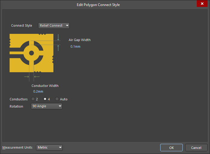 ). As well as applying the settings in the dialog/panel, you must also repour all impacted polygons where the vias connect using a relief style connection. ). As well as applying the settings in the dialog/panel, you must also repour all impacted polygons where the vias connect using a relief style connection. |
| Load Values from Routing Via Style Rule (Add Stitching to Net dlg) |
When you click this button, the properties of the via in the applicable Routing Via Style rule are applied here in the Add Stitching to Net dialog. Learn more about the Routing Via Style design rule. |
| Via Template | When you select a via template from this dropdown list, the properties of that template via are applied here in the Add Stitching to Net dialog. When a template is selected the Library field displays the library that the via template is linked to, and includes the option to Unlink the template from that library. Learn more about Working with Pad Via Templates. |
| Properties – Net | The net that the stitching vias are to connect to. The style of the via connection (relief or direct) is determined by the object that the via is connected to, and the applicable design rules. More on this in the Notes section. |
| Properties – Drill Pair / Via Type | The start and end layers that the stitching vias span in the Z-plane can be configured as required (this span is referred to as the drill pair). The allowed Z-plane span of vias is configured in the Via Types tab of the Layer Stack Manager (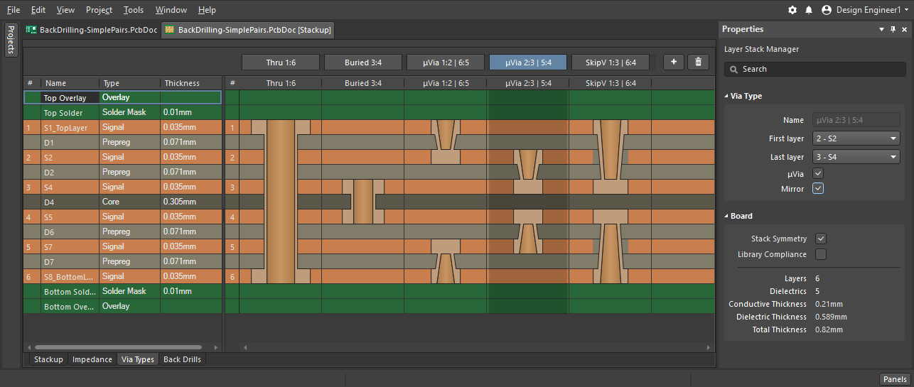 ), only spans defined there will appear in the Drill Pair dropdown. Click the Via Types button to open the Layer Stack Manager, where you can configure the via types available for the active layer stack. Learn more about Via Types. ), only spans defined there will appear in the Drill Pair dropdown. Click the Via Types button to open the Layer Stack Manager, where you can configure the via types available for the active layer stack. Learn more about Via Types. |
| Properties – Locked (Add Stitching to Net dlg) |
If enabled, all of the vias in this set of stitching vias have their Locked attribute enabled. |
| Solder Mask Expansion | Solder mask expansion (or tenting) can either be based on: the applicable Solder Mask design rule, or the expansion value specified here in the dialog (which can be overridden by tenting the via). The option you select is applied to all of the vias in this set of stitching vias. |
 )
)Notes about Via Stitching
-
First select the Net to be used for stitching as this effects the behavior of other options, such as clicking the Load values from Routing Via Style Rule button. If the net is already selected in the design space, that net is automatically chosen when you open the Add Stitching to Net dialog.
-
Shielding vias are identified by VSn: Via Stitching, where the numerical value n identifies this via as belonging to the same via stitching union as other vias with the same numerical identifier.
-
The via connection style (relief or direct) is: defined by the applicable Polygon Connect Style design constraint for polygons, the applicable Plane Connect Style design constraint for power planes, with direct connections for solid regions and fills.
-
Once stitching is complete, you will need to re-pour all impacted polygons where the vias connect using a relief connection style.
-
Each set of stitching vias are added to a union, set the PCB panel to Unions mode to explore these unions (
 ).
).
-
To edit a set of stitching vias, double-click on any via in the set to open the Via Stitching dialog, or the Properties panel if it is configured to open on double-click (
 ). Alternatively, drag a select-within rectangle (left-to-right) that includes one or more stitching vias, then edit the settings in the Properties panel.
-
The set of vias can be removed by running the Tools » Via Stitching » Remove Via Stitching Group command, then clicking on any via in the group.
-
The via stitching algorithm treats polygons, fills, solid regions and power planes in the following way:
-
Polygons, regions and fills that are on the same net are stitched wherever they overlap on different layers. If there are polygons, regions or fills on other nets that are overlapping within that area (on another layer), stitching is not applied in that region. Overlapping plane regions on other nets are passed through.
-
Overlapping plane regions on the target net are always stitched, regardless of the presence of plane regions (on another layer) attached to other nets. Rule 1 above applies if there are polygons, regions or fills overlapping in the same region.
-
Modifying the Via Stitching Area
The set of vias in each unique area of via stitching are clustered into a union. The entire union can be moved, and the area can also be resized.
Drag a left-to-right selection window to select a stitching area, then move or resize by positioning the mouse to get the correct cursor.
Modifying the Via Stitching Area
-
Drag a select-within rectangle (left-to-right) so that it includes one or more of the stitching vias. The boundary of the selected stitching area will be displayed, as shown in the animation above.
-
To move a selected stitching union - position the cursor within the area, when the move cursor
 appears click and hold then move the area to the new location. Note that you can also move a stitching union by clicking and dragging directly on one of the stitching vias, as shown in the animation above.
-
To resize the selected stitching union by moving an edge - position the cursor over the edge, when the move edge cursor
 appears click and hold then slide the edge to the new location.
-
To resize the selected stitching union by moving a vertex - position the cursor over the edge, when the move vertex cursor
 appears click and hold then slide the vertex to the new location.
-
After you release the mouse button you will be prompted to Re-generate via stitching?, click Yes to update the via stitching in the new location/shape, or click No if you have not completed editing the shape.
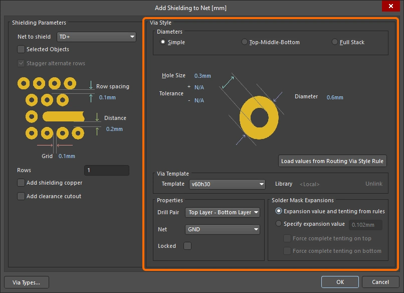
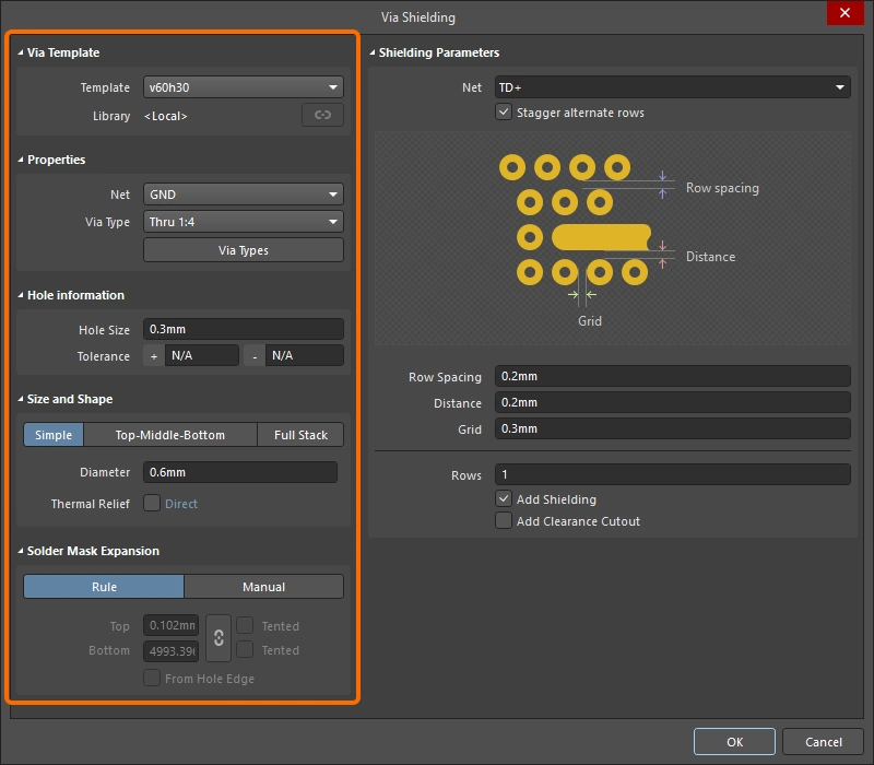
Adding Shielding Vias to a Net
Via shielding is used to isolate a net from potential interference or coupling from nearby signals. The shielding vias must be spaced to suit the highest frequency being protected against. Correct design of the shield is essential; a poorly designed fence could actually contribute to EMI issues if the spacing is at the resonant frequency of a nearby signal. This is discussed more in the Notes about Via Shielding section.
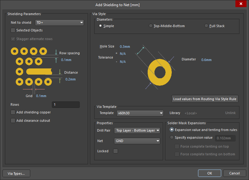
To place a via shield around a routed net, select the Tools » Via Stitching/Shielding » Add Shielding to Net command from the menus. The Add Shielding to Net dialog will appear where you configure the Net to Shield and other Shielding Parameters, the reference Net, and the Via Style as required. The vias will be placed along both sides of the chosen net(s), wherever it is possible to place a via that complies with the applicable design rules.
 )
)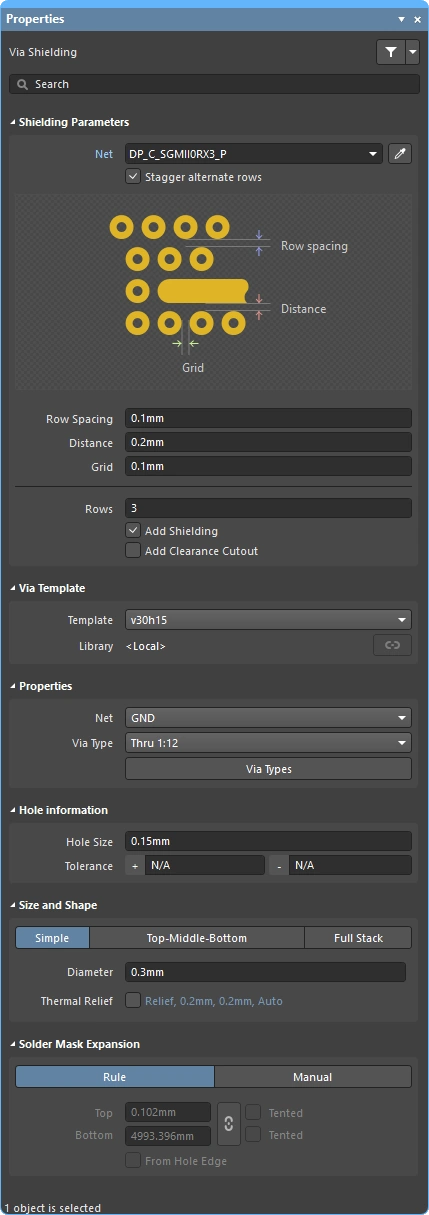 ).
).Shielding Parameters
The shielding parameters control the net(s) being shielded, and the shielding via placement pattern.
Shielding Parameters ( |
|
| Net to shield | The net to have shielding vias placed around. If the net belongs to a defined differential pair, then both nets will be shielded. If the pair of nets is not defined as a differential pair, select them before opening the dialog and use the Selected Objects option instead. |
| Selected Objects (Add Shielding to Net dlg) |
Place shielding vias around the selected objects, rather than the net selected in the Net to shield field. Can also be used to shield multiple selected nets. |
| Stagger alternate rows | Alternate rows of shielding vias are offset by half of the Grid value. |
| Row Spacing | The spacing between rows of shielding vias (edge to edge separation) when the Rows setting is greater than 1. |
| Distance | The separation from the edge of the shielded track segments to the edge of the shielding vias. |
| Grid | The distance between the edges of adjacent shielding vias. Shielding vias will not be placed in violation of applicable design rules; if a potential via site would result in a violation, then that site is skipped. |
| Rows | The number of rows of shielding vias. |
| Add shielding copper | Place a polygon over the area occupied by the shielding vias, connected to the net specified in the Via Style Net field. The polygon is defined in accordance with the applicable Clearance constraint and Polygon Connect Style design constraint. |
| Add clearance cutout | Include a polygon cutout around the shielded net, set back from the net by the distance specified in the Distance field. Use this when you require a different clearance from the applicable Clearance constraint. |
 )
)Via Style
The properties of the shielding vias are displayed in the Via Style region of the dialog. These properties can be defined by:
-
New settings that you enter into the dialog, or
-
Based on the settings of a selected Via Template, or
-
Based on the settings defined in the applicable Routing Via Style design rule, if you are placing a new set of shielding vias.
Via Style ( |
|
| Diameters (Simple/TMB/Full) |
The PCB editor supports 3 types of X-Y plane via diameters: Simple, Top-Middle-Bottom, or Full Stack. Click to select the via structure required for the shielding vias. Learn more about the Via Stack. |
| Hole Size | Specifies the hole size value for the shielding vias. |
| Tolerance | Setting hole tolerance attributes can help determine the fits and limits of your board. Specify the Minimum (-) and Maximum (+) hole tolerance for the shielding vias. |
| Diameter | The diameter of the shielding vias in the X-Y plane. |
| Thermal Relief (Via Shielding dlg & Properties panel) |
Enable the checkbox to allow the definition of local polygon connection style settings for all of the vias in the set, then click the linked keyword to configure the settings in the Edit Polygon Connect Style dialog (). As well as applying the settings in the dialog/panel, you must also repour all impacted polygons where the vias connect using a relief style connection. |
| Load Values from Routing Via Style Rule (Add Shielding to Net dlg) |
When you click this button, the properties of the via in the applicable Routing Via Style rule are applied here in the Add Shielding to Net dialog. Learn more about the Routing Via Style design rule. |
| Via Template | When you select a via template from this dropdown list, the properties of that template via are applied here in the Add Shielding to Net dialog. When a template is selected the Library field displays the library that the via template is linked to, and includes the option to Unlink the template from that library. Learn more about Working with Pad Via Templates. |
| Properties – Net | The net that the shielding vias are to connect to. The style of the via connection (relief or direct) is determined by the object that the via is connected to, and the applicable design rules. More on this in the Notes section. |
| Properties – Drill Pair / Via Type | The start and end layers that the shielding vias span in the Z-plane can be configured as required (this span is referred to as the drill pair). The allowed Z-plane span of vias is configured in the Via Types tab of the Layer Stack Manager (), only spans defined there will appear in the Drill Pair dropdown. Click the Via Types button to open the Layer Stack Manager, where you can configure the via types available for the active layer stack. Learn more about Via Types. |
| Properties – Locked (Add Shielding to Net dlg) |
If enabled, all of the vias in this set of shielding vias have their Locked attribute enabled. |
| Solder Mask Expansion | Solder mask expansion (or tenting) can either be based on: the applicable Solder Mask design rule, or the expansion value specified here in the dialog (which can be overridden by tenting the via). The option you select is applied to all of the vias in this set of shielding vias. |
 )
)Notes about Via Shielding
-
Select the Net to be shielded first as this affects the behavior of other options, such as clicking the Load values from Routing Via Style Rule button. If the net is already selected in the design space, that net is automatically chosen when you open the Add Shielding to Net dialog.
-
Shielding vias are identified by VSHn: Via SHielding, where the numerical value n identifies this via as belonging to the same via shielding union as other vias with the same numerical identifier.
-
The via connection style (relief or direct) is: defined by the applicable Polygon Connect Style design constraint for polygons, and the applicable Plane Connect Style design constraint for power planes.
-
Once stitching is complete, you will need to re-pour all impacted polygons that have an applicable Polygon Connect Style design rule specifying a relief connection style.
-
Each set of shielding vias are added to a union, set the PCB panel to Unions mode to explore these unions (
 ).
).
-
To edit a set of shielding vias, double-click on any via in the set to open the Via Shielding dialog, or the Properties panel if it is configured to open on double-click (
). Alternatively, drag a select-within rectangle (left-to-right) that includes one or more shielding vias, then edit the settings in the Properties panel.
-
The set of vias can be removed by running the Tools » Via Stitching/Shielding » Remove Via Shielding Group command, then clicking on any via in the group.
-
You can perform partial net shielding or multi-net shielding:
-
If you do not want to shield the entire net, select the required track segments first, then shield with the Selected Objects option enabled.
-
To shield multiple adjacent nets, select the nets in the design space, and then shield with the Selected Objects option enabled.
-
Note that a differential pair can be shielded using the multiple-net Selected Objects technique, or by choosing either one of the differential pair nets in the Net to Shield dropdown.
-
-
Use the Add shielding copper option to add a polygon that encloses the shielding vias, include the Add clearance cutout option to clip the polygon back to just enclose the vias. Read the Including Shielding Copper with the Shielding Vias topic below to learn more about these options.
Including Shielding Copper with the Shielding Vias
As well as adding shielding vias along each side of the routing, you can also include shielding copper, as shown in the images below. To do this, enable the Add shielding copper option in the Via Shielding dialog. This copper is created as a polygon, so it obeys the applicable Clearance and Polygon Connect Style design rules.
The Add shielding copper option will add a polygon that encloses the shielding vias. The polygon edge that is away from the shielded net will touch the edge of the vias. The polygon edge that is adjacent to the shielded net will be set back from the net by the applicable Clearance design rule. If the Add clearance cutout option is also enabled, the polygon will instead be set back from the shielded net by the Distance setting in the Add Shielding to Net dialog. Hover the cursor over the image below to see the difference.

Selecting or Editing Stitching or Shielding Vias
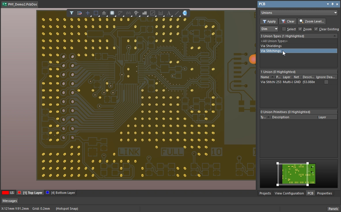
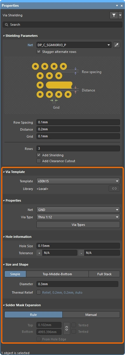
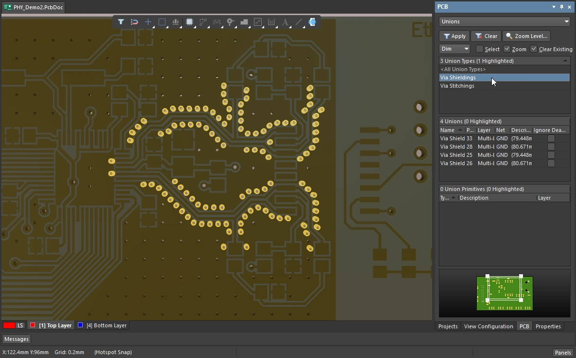
To simplify the process of working with an array of stitching/shielding vias, both kinds are automatically clustered into a union. Unions are managed through the PCB panel.
Selecting using the PCB Panel
To select the array, switch the PCB panel to Unions mode and select the required Via Stitching or Via Shielding union. All vias that are part of that array will select if the Select checkbox is enabled in the panel (as shown in the image below). Alternatively, double click on any via in the array to open the Properties panel and edit the array.
Use the PCB panel in Unions mode to select all vias in a stitching or shielding array. In this image, all four via shielding unions are selected.
Interactively Selecting a Via Set
Selection behavior:
-
An individual stitching/shielding via can be selected and deleted.
-
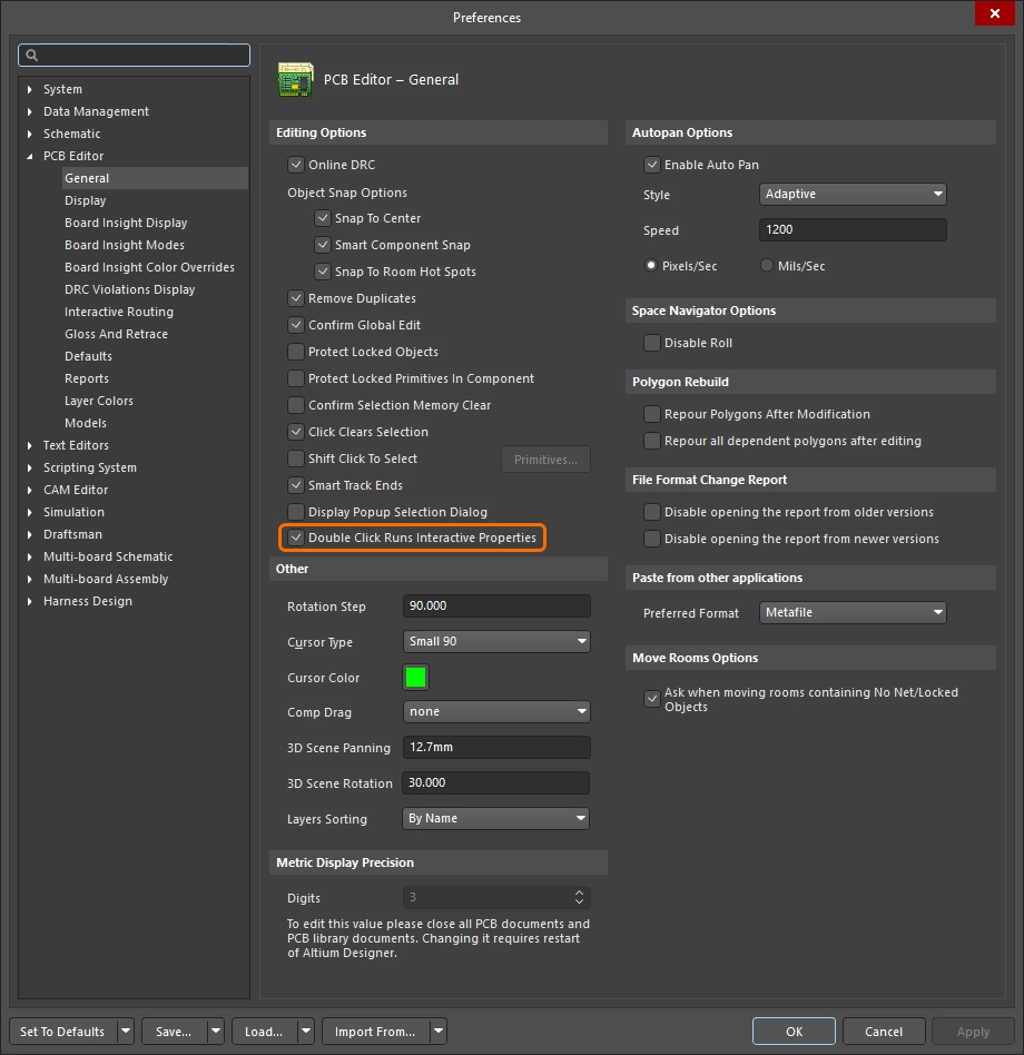
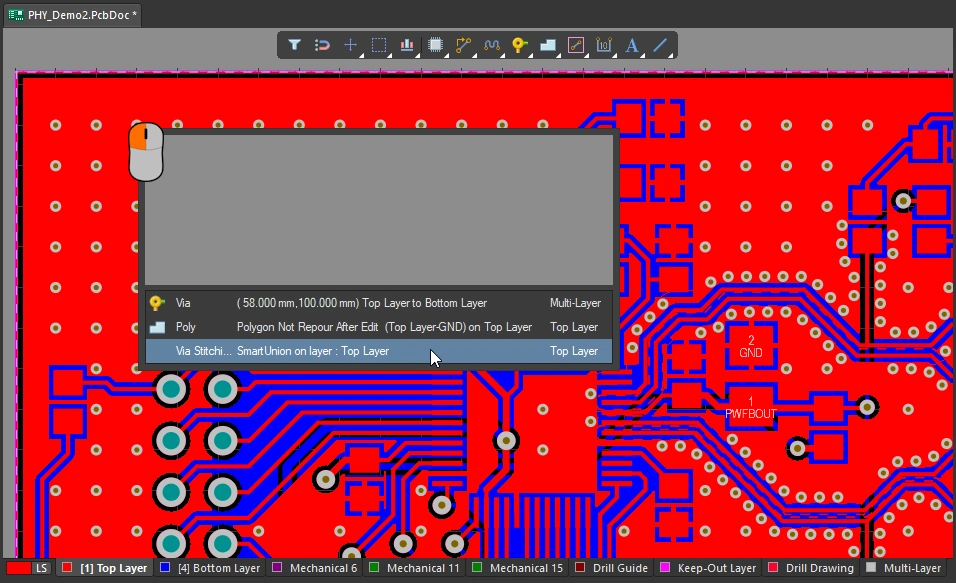
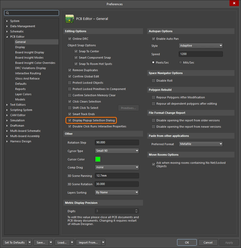
If the Popup Selection Dialog option is enabled in the Preferences (
 ), clicking on an individual via that belongs to a union will display a list that includes the union, as shown in the image above. When a union is selected, that union of vias can be deleted in the workspace, or edited in the Properties panel.
-
If the Popup Selection dialog is not enabled, then clicking on an individual via that belongs to a union will behave in the following way:
-
The first click will select the individual via.
-
The second and subsequent clicks will select the next object in the selection order used when there are overlapping objects: for example, component, polygon, via union (if those objects are under the cursor).
-
Alternatively, after the first click selects the individual via, press the
Shift+Tabshortcut to invoke the Select Overlapping command. Continue pressingShift+Tabto cycle through the overlapping objects, selecting each in turn.
-
-
A stitching union that is constrained to an area can be selected by dragging a select-within window around any via in the union (drag left-to-right), as demonstrated in the animation in the Modifying a User-Defined Via Stitching Area section of this page.
Editing a Via Set
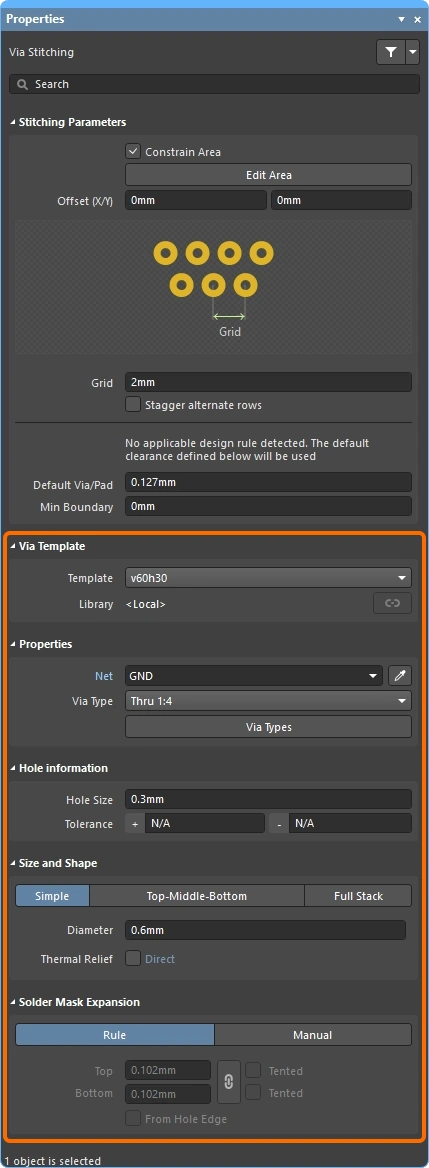
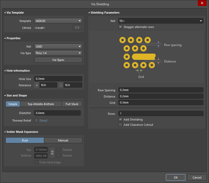
The properties of a stitching or shielding via set can be edited once it has been selected, in the Via Stitching or the Via Shielding mode of the Properties panel. Double-click on any via in the set to open the panel.
 An example of an edit being performed to stitching vias in the Properties panel.
After you edit a property in the panel and press Enter on the keyboard, the Changes pending message and buttons appear at the top of the panel - click Apply to complete your editing action.
Further Reading
-
For information about all aspects of PCB design, refer to the Printed Circuit Design and Fab Magazine website. The site is an excellent resource for technical topics, such as the role of a "via fence" (include the quote marks to improve the quality of the search results).
-
Wikipedia article, Via Fence
-
Studies on Via Coupling on Multilayer Printed Circuit Boards
-
A paper that introduces the basic principals of EM wave propagation within a PCB structure - Best practice in circuit board design
-
A discussion forum where the question Via fences for noise reduction of a chip antenna? was asked