
Differential Pair Routing

A differential signaling system is one where a signal is transmitted down a pair of tightly coupled carriers, one of these carrying the signal, the other carrying an equal but opposite image of the signal. Differential signaling was developed to cater for situations where the logic reference ground of the signal source could not be well connected to the logic reference ground of the load. An advantage of differential signaling is that it is inherently immune to common mode electrical noise, the most common interference artifact present in an electronic product. Another advantage of differential signaling is that it minimizes electromagnetic interference (EMI) generated from the signal pair.
Differential Pair PCB Routing
Differential pair PCB routing is a design technique employed to create a balanced transmission system able to carry differential (equal and opposite) signals across a printed circuit board. Typically, this differential routing will interface to an external differential transmission system, such as a connector and cable.
It is important to note that while the coupling ratio achieved in a twisted pair differential cable may be better than 99%, the coupling achieved in differential pair routing will typically be less than 50%. Current expert opinion is that the PCB routing task is not to simply try and ensure a specific differential impedance is achieved, rather, to focus on ensuring the differential signal arrives in good condition at the target component as it travels from the external cabling.
According to Lee Ritchey, a noted industry high-speed PCB design expert, successful differential signaling requires:
-
Setting each of the routing signal impedances to half the incoming differential cable impedance.
-
That each of the two signal lines is properly terminated in its own characteristic impedance at the receiver end.
-
That the two lines should be of equal length, to within tolerances of the logic family and the circuit frequency used in the design. The primary focus should be on preserving the timing; match the lengths to satisfy the skew budget of the design. For example, for USB 3.x the length mismatch should be no greater than 10 mils.
-
Use the benefit of routing the two signals side-by-side to help achieve good quality routing of matched lengths. Where required, it is acceptable to separate to route around obstacles.
-
Layer changes are acceptable as long as the signal impedances are maintained.
Defining Differential Pairs During Design Capture
The approach you use to defining the differential pairs during design capture depends on how you plan to implement the design constraints for the project. Altium Designer supports two approaches to this. The first is to define the constraints as PCB design rules, in the PCB editor. The second approach is to use the Constraint Manager, a spreadsheet-like interface that allows you to start defining many of the constraints during design capture.
Defining the Differential Pairs on the Schematic Sheet
The PCB design rules approach requires most of the constraints to be defined during PCB design; however key constraints, including the definition of differential pairs, can be defined during design capture by placing schematic design directives.
 Differential pairs can be defined directly on the schematic sheet using a combination of net naming and differential pair directives.
Using Differential Pair Directives on the Schematic ( |
|
| Identify pairs through net names, | Altium Designer requires two things to identify the nets that belong to a differential pair. The first is a net naming convention that uses a common net name with a standard pair-identifying suffix, (eg DRV1_L & DRV1_H). The suffix-pair must be declared in the Options tab of the Options for Project dialog (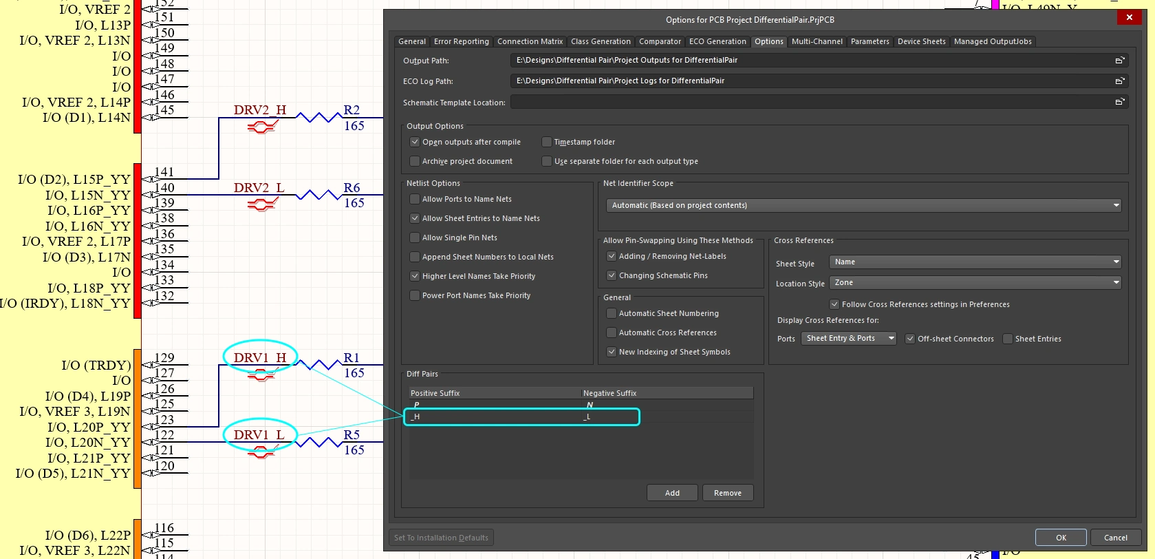 ). ). |
| then identify each pair side using Differential Pair directives | The second element of the graphical approach to defining a differential pair is to place a Differential Pair directive on each net in the pair (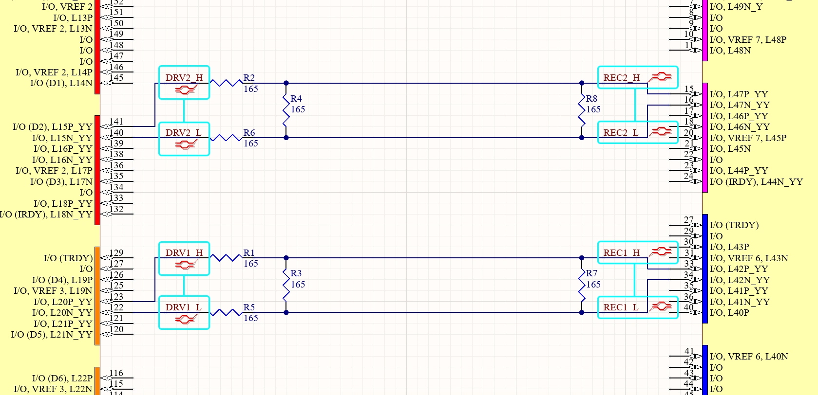 ). ). |
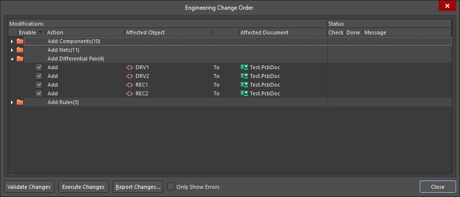
| Transfer the Differential Pairs to the PCB | When the design is transferred to the PCB editor (Design » Update PCB), the schematic differential pairs will be detected and defined in the PCB ( |
 ).
).Defining the Differential Pairs in the Constraint Manager
If the design uses the Constraint Manager, the nets in the pair are also identified by a common name with a pair-identifying suffix, but the differential pair directive is not required. The Constraint Manager also supports the definition of logical xNets. An xNet (extended net) is a feature used to define a continuous, intelligent signal path that spans across passive, series-termination components, such as resistors or capacitors, treating the entire path from driver to receiver, including the component, as one logical net for length matching and constraint management.
 In this example an xNet has been defined for the complete driver-to-receiver path of each signal, and then differential pairs created from these xNets.
Defining Differential Pairs in the Constraint Manager |
|
| Identify pairs through net names | Identify the nets in a differential pair using a common net name with a standard pair-identifying suffix, (eg |
| Where the constraints are defined | Constraints are created and edited in the Constraint Manager (a separate editor from the schematic editor), and the constraints are stored in a specific constraints file. Learn more about the Constraint Manager. |
| Keeping the constraints and schematic in sync | Because the constraints are stored separately from the schematic, changes made in the Constraint Manager must be saved before they are reflected on the schematic (and can be synchronized to the PCB). Design changes made in the schematic are imported into the Constraint Manager by clicking the Refresh button (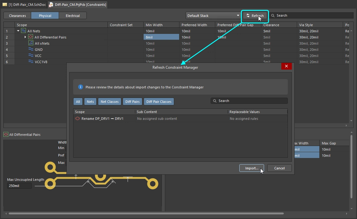 ). ). |
| If the design still includes Differential Pair directives | Graphical differential pair directives are not required if the Constraint Manager is used. If Differential pair directives are detected when a Refresh is performed, they are converted into a differential pair constraint that is then managed and edited in the Constraint Manager. This change of state is reflected on the schematic by changing the color of the symbol and adding a small letter c to it (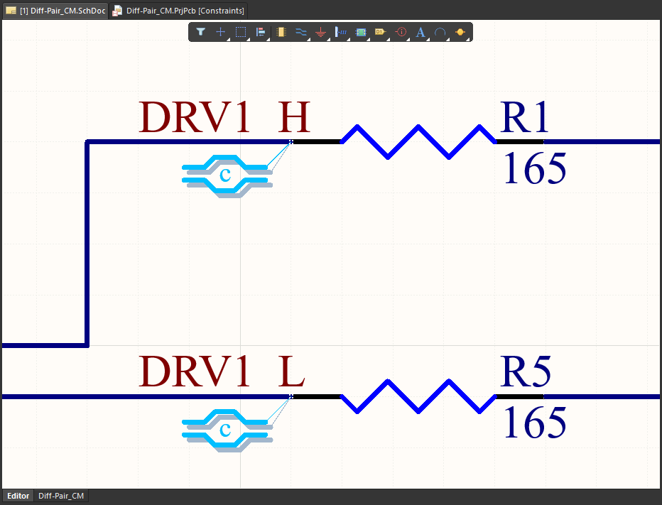 ). Once they have been converted those settings are managed in the Constraint Manager. Learn more about importing directives from the schematics. ). Once they have been converted those settings are managed in the Constraint Manager. Learn more about importing directives from the schematics. |
| Identify pairs using the Constraint Manager | The Constraint Manager can create differential pairs based on their net names and suffix, whenever the right-click » Differential Pairs » Create Differential Pairs from Nets command is selected (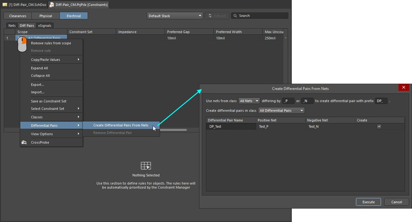 ). Learn more about defining differential pairs in the Constraint Manager. ). Learn more about defining differential pairs in the Constraint Manager. |
| Create an xNet to define the entire signal | An xNet (extended net) is a feature used to define a continuous, intelligent signal path that spans across passive, series-termination components, such as resistors or capacitors. An xNet treats the entire path from driver to receiver – including the component – as one logical net for length matching and constraint management. Learn more about defining xNets in the Constraint Manager. |
| Create xSignals to control the net topology | If required, the net topology can also be defined and stored as an xSignal, which can be synchronized to the PCB. Learn more about defining xSignals in the Constraint Manager. |
| Transferring the Differential Pairs to the PCB | Differential pairs (as well as xNets and xSignals) are transferred to the PCB during design synchronization if the relevant settings in the Options for PCB Project dialog are enabled (on by default). Learn more about the options for a PCB project. |
Learn more about Defining Design Requirements Using the Constraint Manager
Learn more about Working with Classes
Viewing and Managing Differential Pairs on the PCB
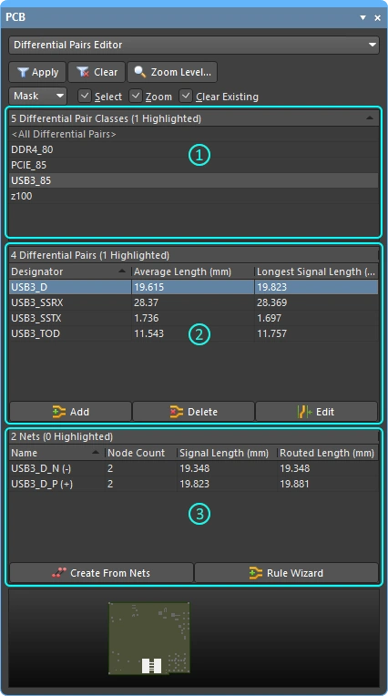
In the PCB editor, differential pair definitions are viewed and managed in the PCB panel in Differential Pairs Editor mode.
In Differential Pairs Editor mode, the three main regions of the panel are used to review and manage the differential pairs in the current PCB design:
-
Differential Pair Classes – a list of all differential pair classes currently defined for this board. The
USB3_85class is selected. Double-click to edit the class, or right-click to define a new class. Differential pair classes are an optional design management feature. -
Differential Pairs – all of the differential pairs that are in the currently selected differential pair class (in the first region of the panel). The
USB3_Ddifferential pair is selected in the example image. -
Nets – the constituent (negative and positive) nets that are in the currently selected differential pair. The nets in this pair are
USB3_D_NandUSB3_D_P. The - and + displayed next to each pair member's net name is a system flag indicating if it is the positive or negative member of the pair. Right-click to control which columns are visible in this section of the panel (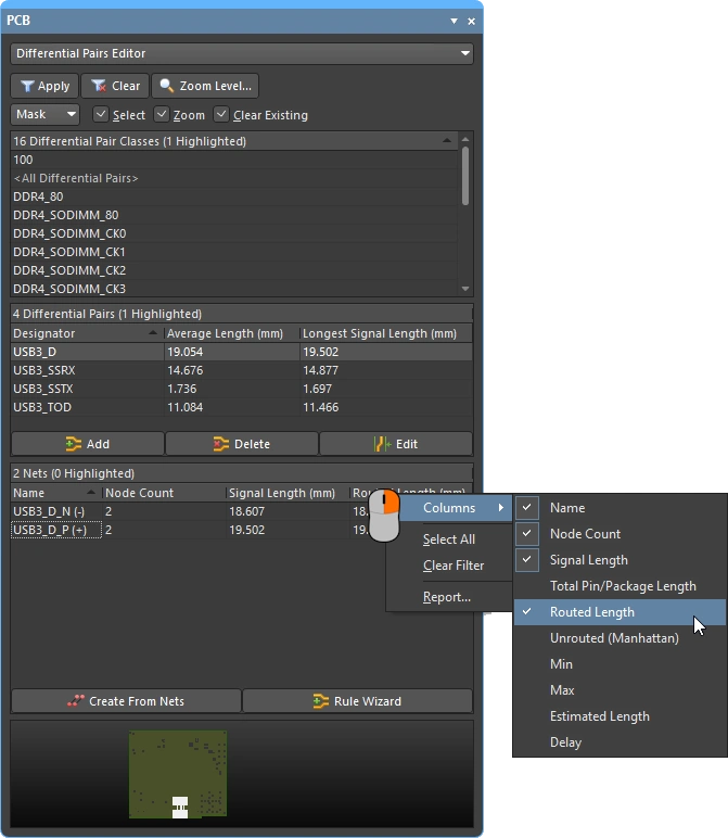 ) there is a definition of each column below.
| Manually creating a new pair | To manually create a new differential pair object directly in the PCB editor, click the Add button in the Differential Pair region of the PCB panel (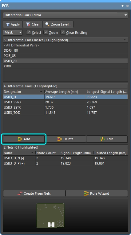 ). The Differential Pair dialog will open ( ). The Differential Pair dialog will open ( ), select existing nets for both the positive and negative nets, name the pair, then click OK. Note that only available nets are listed for selection, any nets that are currently defined as part of an existing differential pair are not listed. ), select existing nets for both the positive and negative nets, name the pair, then click OK. Note that only available nets are listed for selection, any nets that are currently defined as part of an existing differential pair are not listed. |
| Edit a pair definition | To edit an existing pair, double-click on the name in the Differential Pair region of the PCB panel, or select it and click the Edit button (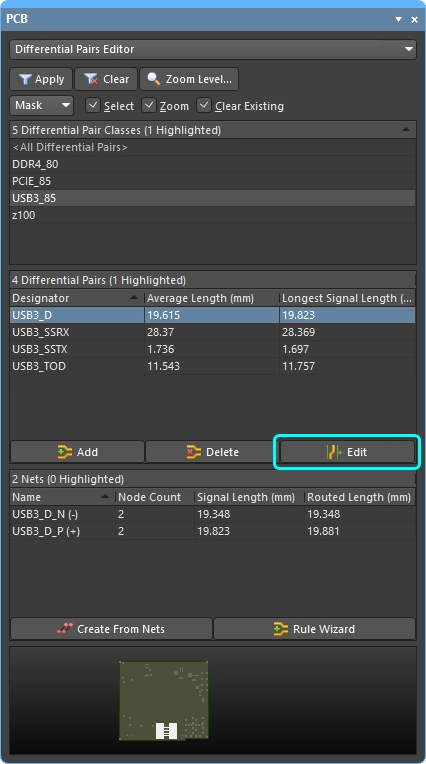 ). ). |
| Delete a pair | To delete an existing differential pair, select its entry and click the Delete button in the panel (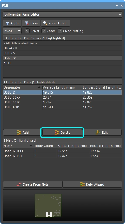 ). ). |
| Creating pairs from the design nets | If you are pairing nets that have a consistent naming scheme (i.e. they have a common prefix and a consistent positive/negative suffix such as, TX0_P and TX0_N), you can use the Create Differential Pairs From Nets dialog (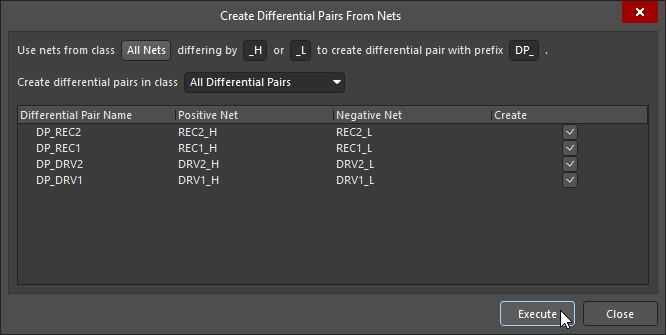 ). Click the Create From Nets button in the PCB panel ( ). Click the Create From Nets button in the PCB panel (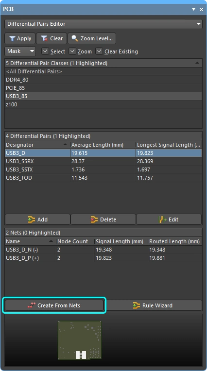 ) to open the dialog. The dialog will automatically list all existing nets that comply with the filter settings at the top of the dialog. Configure the filter settings and assign the differential pair class if required. For any proposed pair that is not required, clear the Create checkbox. ) to open the dialog. The dialog will automatically list all existing nets that comply with the filter settings at the top of the dialog. Configure the filter settings and assign the differential pair class if required. For any proposed pair that is not required, clear the Create checkbox. |
| Creating pairs using the wizard | Clicking the Rule Wizard button (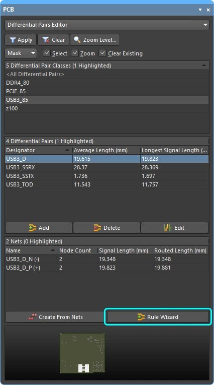 ) will launch the Differential Pair Rule Wizard, this is documented later on this page. ) will launch the Differential Pair Rule Wizard, this is documented later on this page. |
| Create a differential pair class in the panel | To create a new differential pair class, right-click in the Differential Pair Classes region of the panel and select Add Class from the context menu (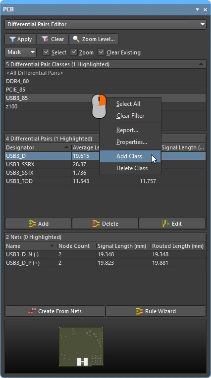 ). The Edit<ObjectKind>Class dialog will open, where you can enter a name for the class and add members. ). The Edit<ObjectKind>Class dialog will open, where you can enter a name for the class and add members. |
| Edit a differential pair class | Double-click on an existing class to open the Edit<ObjectKind>Class dialog, where you can edit its name or add/remove members. |
| Manage classes in the Object Class Explorer | For full control and editing of all classes, including differential pair classes, select the Design » Classes command to open the Object Class Explorer dialog (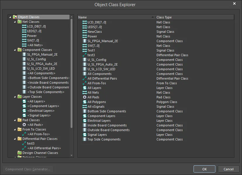 ). Learn more about defining classes in the PCB editor. ). Learn more about defining classes in the PCB editor. |
Differential Pair Editor – Definition of Columns
| Average Length | Calculated average of the Routed Lengths of the two nets in the pair. |
| Longest Signal Length | The Signal Length of the longer of the two nets in the pair. |
| Name | Name of the signal. |
| Node Count | total number of pads in this signal. |
| Routed Length | The sum of the lengths of the placed track and arc segments that form the routing, plus the vertical distance traversed through vias (see note below). The routed length calculator does not attempt to resolve overlapping track segments or routing wiggles inside pads. |
| Signal Length | Accurate calculation of the total node-to-node distance. Placed objects are analyzed to: resolve stacked or overlapping objects and wandering paths within pads; and via lengths are included. If the net is not completely routed the Manhattan (X + Y) length of the connection line is also included. |
| Estimated Length | The Routed Length plus the length of connection lines for any section still to be routed. It does not use the Manhattan length for the unrouted portion; instead it uses the direct point to point distance. |
| Total Pin/Package Length | The sum of all the Pin Package Length values in all pads in that xSignal. This value is defined as a property of the PCB pad and can also be specified in the schematic pin. |
| Unrouted (Manhattan) | The vertical plus horizontal (X+Y) distance of all unrouted sections. |
| Min / Max | Derived from the applicable Length and Matched Length design rules. If there is no applicable rule(s) defined, the internal defaults of Min=0mil and Max=99999mil are used. |
| Delay | The time it takes for a signal to propagate along that route. |
Design Constraints
In Altium Designer, the properties of the objects placed in the design are controlled by design constraints. Constraints are used to both instruct the creation tools, such as the width for routing and the gap between pair members during differential pair routing; and are also used during design rule verification to confirm that the placed objects meet the design requirements.
As mentioned earlier, design constraints are either defined through the Constraint Manager, or as PCB design rules. While these techniques use a different approach to create and manage the constraints, the set of available constraints is the same in the Constraint Manager and the PCB rules, as is the underlying approach used to target the design constraint to the objects that it should apply to.
Behind the user interface, Altium Designer uses a filtering engine to target the objects that a design constraint applies to, driven by a query system. The query system identifies objects using query functions, such as IsComponent('U1'), or InAnyDifferentialPair. The process of creating a query to target the required objects is called setting the scope of the design constraint. In many of the places where the constraint is scoped you will choose an option from a dropdown list, which the PCB editor converts into a suitable query. For a more specific constraint, such as all nets (except pairs) under this BGA, you will need to construct the query from suitable query functions, for example WithinRoom('RoomDefinition_BGA') and Not InAnyDifferentialPair.
In a rules-based project the query for any constraint can be examined by switching the Object Matches scope in the constraint to Custom Query (in the PCB Rules and Constraint Editor), as shown in the third slide below. In a Constraint Manager-based project, open the Constraint Manager from the PCB editor and switch to All Rules to display the query behind a constraint (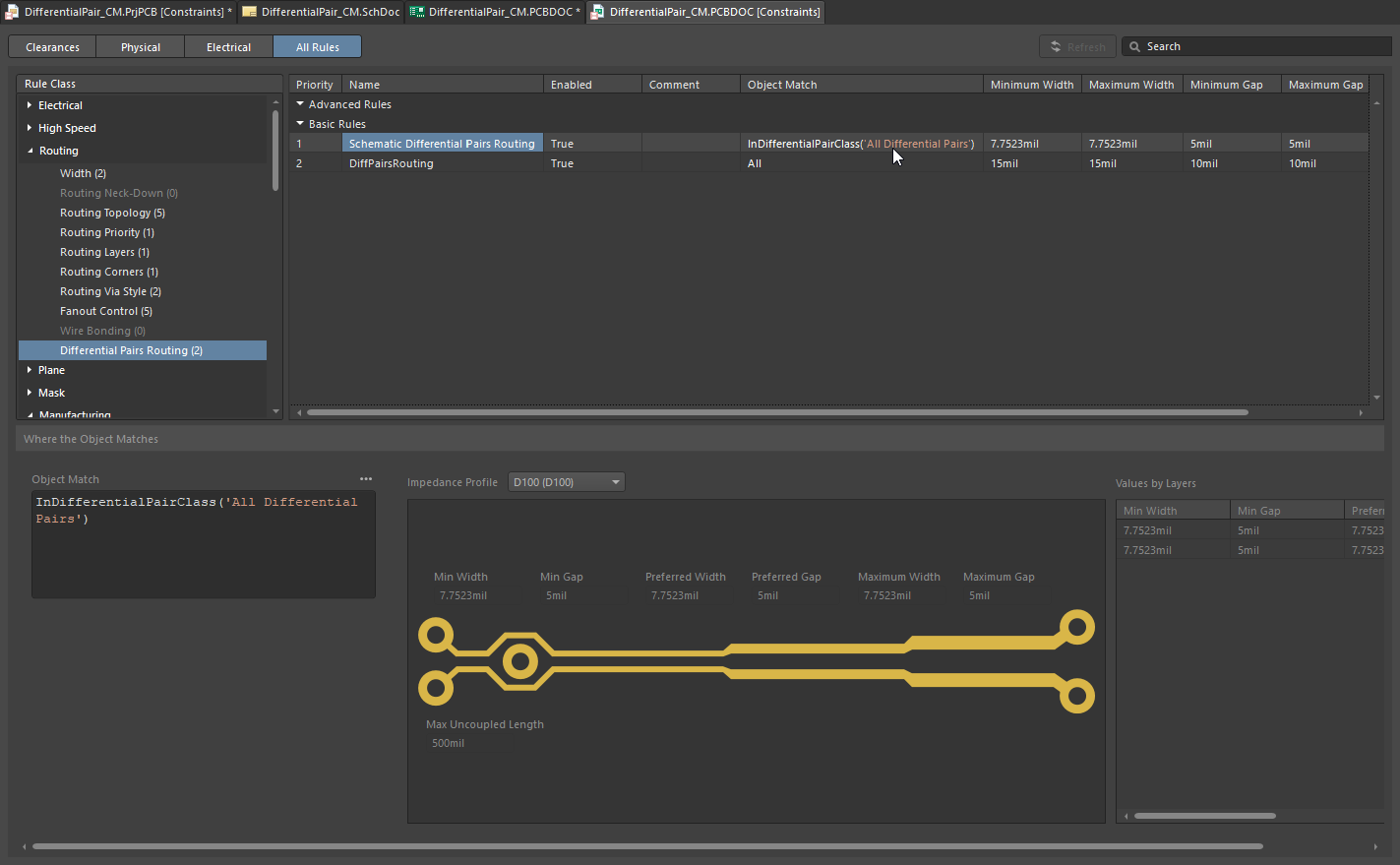 ).
).
Learn more about the query language.
Setting the Scope of the Design Constraint
The scope of the design rule defines the set of objects that you want the rule applied to. Since a differential pair is an object, you can use queries like the following examples:
Query Keywords to target Differential Pairs |
|
InAnyDifferentialPair |
Is the object in any differential pair. |
InDifferentialPair('D_V_TX1') |
Targets both nets in the differential pair named D_V_TX1. |
InDifferentialPairClass('ROCKET_IO_LINES') |
Targets all nets in all pairs belonging to the differential pair class called ROCKET_IO_LINES. |
(IsDifferentialPair And (Name = 'D_V_TX1')) |
Targets the differential pair object that has a name of D_V_TX1. |
(IsDifferentialPair And (Name Like 'D*')) |
Targets all differential pair objects whose name starts with the letter D. |
Learn more about the available PCB query functions.
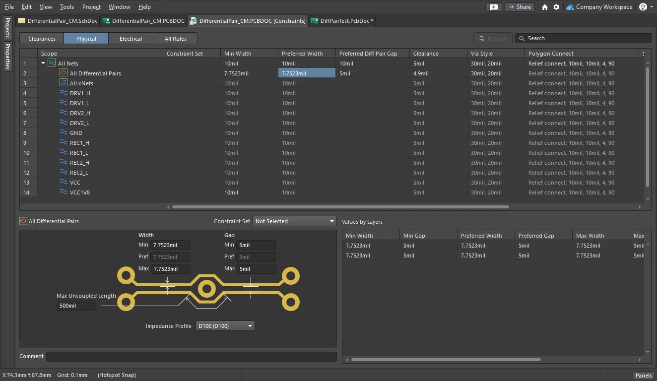
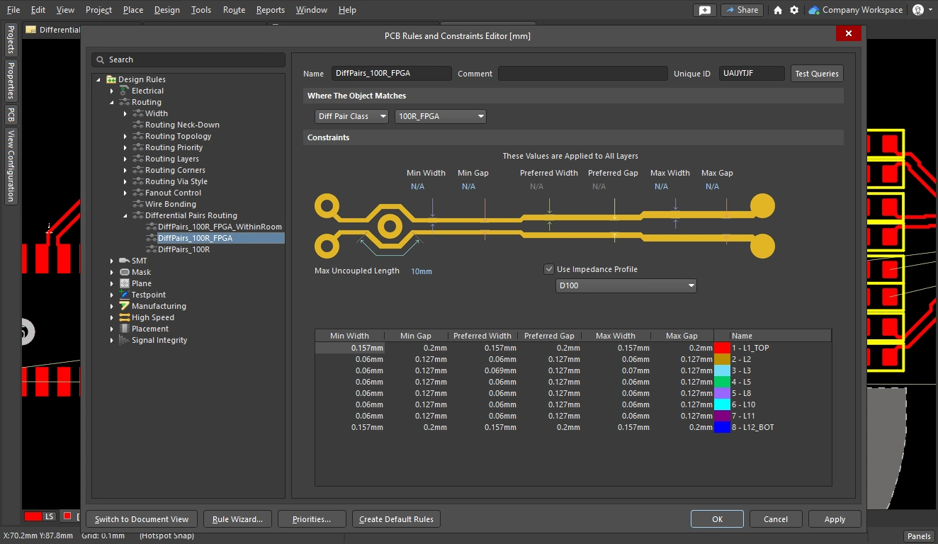
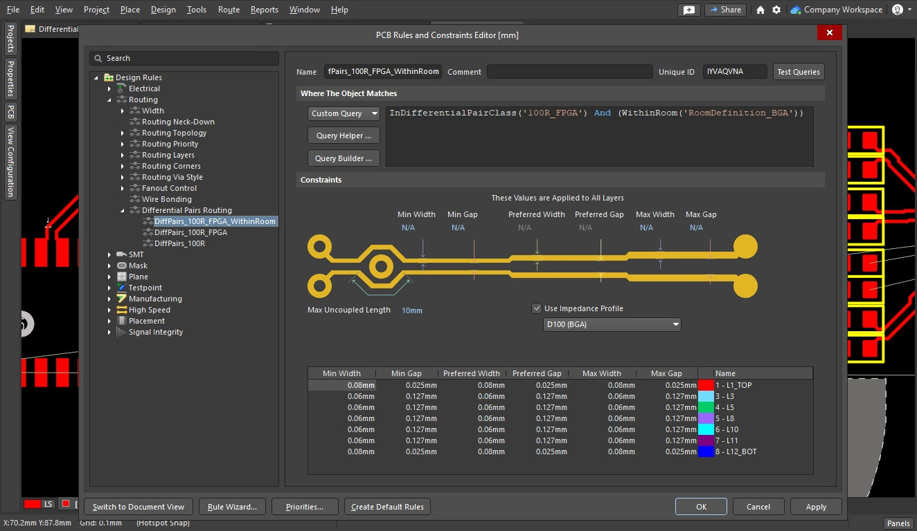
Differential Pair Routing Constraint
The key objectives for routing a differential pair are to route each net in the pair at the preferred width, while keeping them separated by the preferred gap. The example images below show this being done for All Differential Pairs, the first using the using the Constraint Manager, the second using the PCB Rules and Constraints Editor. The width and gap are defined as numerical values. Alternatively, a differential pair impedance profile can be defined in the Layer Stack Manager and this profile chosen in the constraint, as shown below. This page includes a summary of key elements of the constraint, use the link below for more details about the constraint.
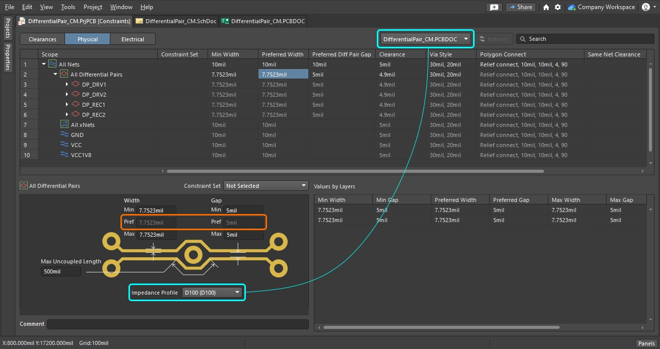
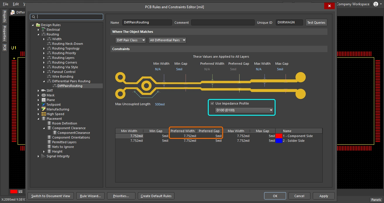
Constraining a Differential Pair |
|
| Measurement units | The units default to the board units, use the Ctrl+Q shortcut to switch them between imperial and metric in the dialog / editing window you are currently viewing. In the Constraint Manager, the units can also be switched via the Tools menu. |
| Routing width | Enter the Min, Preferred and Max Widths as a numerical value. Use the 3 shortcut to cycle between these settings during interactive differential pair routing, the current state is reported on the Status bar and in the heads-up display. |
| Gap between nets in the pair | Enter the Min, Preferred and Max Gaps as a numerical value. Use the Shift+6 shortcut to cycle between these settings during interactive differential pair routing, the current state is reported on the Status bar and in the heads-up display. |
| How the Gap is checked | The Preferred Gap value is used by the Interactive Differential Pair routing tool as track segments are placed during routing. However, the distance between all electrical objects is checked by the applicable Clearance Constraint. In the Design Rules dialog this is configured as a separate design constraint ( |
| Settings based on an Impedance profile | This approach requires the impedance profile to have been configured in the Layer Stack Manager. If there are impedance profiles defined, the profile can be selected in the Constraint Manager (first image above) or the rules dialog (second image above). Learn more about configuring an impedance profile. |
Learn more about the Differential Pair Routing Constraint.
Using the Differential Pair Wizard to Define the Constraints
If you are creating the differential pair routing constraints in the PCB editor, as well as doing that manually you can also use the Differential Pair Rule Wizard to walk through the process of adding and configuring a differential pair routing constraint, and a matched length constraint. Click the Rule Wizard button () to launch the Wizard.

The Differential Pair Rule Wizard guides you through the rule definition process.
Note that the scope of the constraints that are created will depend on the current differential pair selection in the PCB panel prior to launching the wizard, as follows:
Constraint Scope |
|
Select the All Diff Pair class (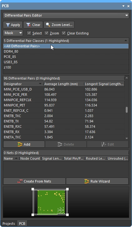 ) ) |
If the All Differential Pairs class is selected, the scope will be All for each rule. |
Select one Diff Pair class (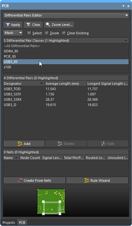 ) ) |
If a specific differential pair class is selected, the scope will be InDifferentialPairClass('ClassName') for each rule. |
Select one Diff Pair (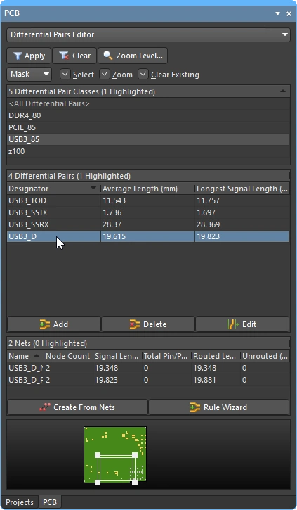 ) ) |
If a single differential pair is selected in the panel, the scopes will be |
Select multiple Diff Pairs (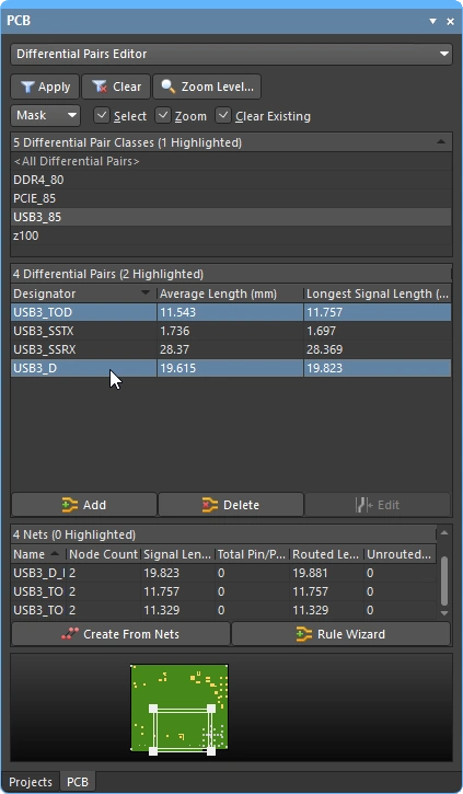 ) ) |
If multiple differential pairs are selected in the panel there will be individual scope entries for each pair object, each separated by an For example, a routing Width rule targeting individually selected differential pair objects |
Using xSignals with Differential Pairs
If your differential pairs have series components in the signal path, you might find it worthwhile to create xSignals. An xSignal is a designer-defined signal path between two nodes. They can be two nodes within the same net, or two nodes in different nets – using an xSignal allows you to define the signal path so that it includes the net on either side of a series component. Route length calculations for xSignals include the length of the path through the series component, as shown by the thin line that is displayed when an xSignal is selected in the xSignals mode of the PCB panel.
 These differential pairs have been defined as xSignals; the route length includes the series component.
Routing a Differential Pair
Differential pairs are routed as a pair - that is, you route the two nets simultaneously. To route a differential pair, select Interactive Differential Pair Routing from the Route menu or the Active Bar. You will be prompted to select one of the nets in the pair; click on either net to start routing. It doesn't matter if the positive or negative trace in a pair is selected as the system will automatically select the other trace too. The video below shows a simple demonstration of differential pairs being routed.
During differential pair routing, you can perform the following functions:
Routing a Differential Pair |
|
| Configuring the router | To change the interactive differential pair routing settings during routing, press |
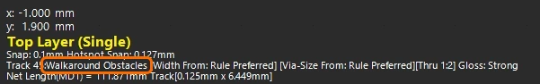
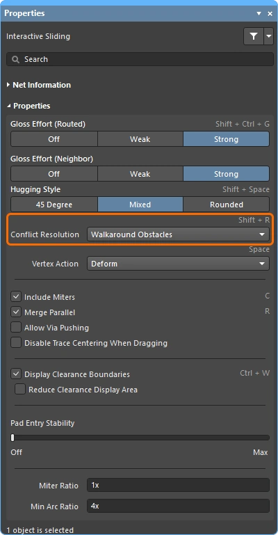
| How the routing reacts to existing objects | This is determined by the current setting of the Conflict Resolution Mode (Walkaround, Push, Hug and Push, Stop at First Obstacle, Ignore Obstacles). The current conflict resolution mode is displayed on the Status bar ( Learn more about the conflict resolution mode during interactive routing. |
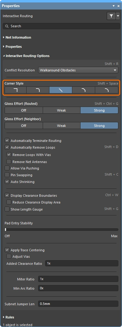
| The shape of the corners | During differential pair interactive routing, the shape formed by the tracks and arcs that create a corner is referred to as the corner style. Diagonal corners are the most common, but curved corners (created by placing arcs), are also popular. There are 5 available corner styles, 4 of which also have corner direction sub-modes.
|
| Controlling the routing width and pair gap | During differential pair interactive routing:
|
| Placing the hatched track segments | Left mouse click to place all of the proposed (hatched) track/arc segments. |
| Unwind the placed routing | Press the Backspace key to remove the last placed vertex. |
| Switch layers and insert a via pair | To change layers during routing, use the
|
| Displaying the available clearance | Wondering why the routing won't fit through that gap? To help with this, press Ctrl+W during routing to enable the dynamic display of clearance boundaries. The no-go clearance area defined by the existing objects + the applicable clearance rule is displayed as shaded polygons (Ctrl+W to toggle the feature off again. |
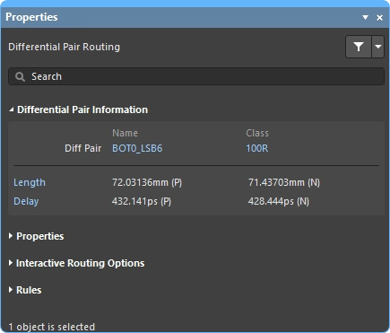
| Panel – Differential Pair Information | Details the name of the differential pair being routed, and the differential pair class (if the pair belongs to one). Also displays the signal length and delay of each net in the pair, this detail is updated at each click event during routing. The blue text in the panel are links, press Learn more about the differential pair panel information. |
| Panel – Properties | During differential pair routing, the properties of the route objects can be edited in the Routing Properties section of the Properties panel. Learn more about the differential pair Properties panel information. |
| Panel – Interactive Routing Options |
Learn more about the differential pair Routing Options panel information. |
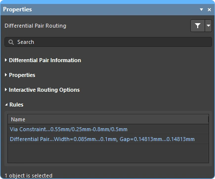
| Panel – Rules | Displays the Routing Width and Routing Via Style design constraints that apply to the pair being routed ( Learn more about the differential pair Rules panel information. |
| Get help on shortcuts | Press Shift+F1 to display all of the available in-command shortcuts. |
 )
) ).
). ).
). ).
).The Quick Differential Pair Routing Tool
For designers whose designs are less demanding there is also a pair of quick routing commands. The Quick Routing tool helps maximize routing efficiency and flexibility in an intuitive way, including following cursor path for laying route sections, single-click routing completion, pushing or walking around obstacles, and automatically following existing connections, all in accordance with applicable design rules.
The Quick Differential Pair Routing command (accessed from the main menu and the Active Bar) offers lighter routing with less settings and capabilities, suitable for simpler designs. Its general behavior and shortcuts are the same as the standard Interactive Differential Pair Routing command.

Summary of Capabilities |
|
| Includes | Capabilities include:
|
| Does not support | This router is referred to as Quick because it offers a reduced feature-set. Features that are not included in the Quick Router include:
If you need any of these features, use the Interactive Differential Pair Routing tool. |
The PCB editor also includes a single-net Quick Route tool, offering similar options and controls as the Quick Differential Pair Routing tool - learn more.
Interactively Modifying the Differential Pair Routing
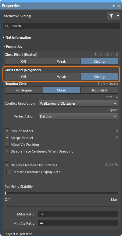
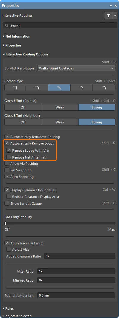
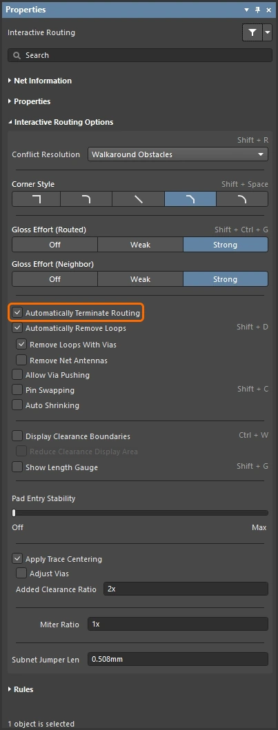
During routing there will be many instances where you need to change some of the existing routing. You can change the routing using a drafting style approach of clicking and dragging on a track segment or via – this is called interactive sliding. To recognize the members of the pair during sliding, the concept of coupling is used. Interactive Sliding controls display in the Properties panel during sliding (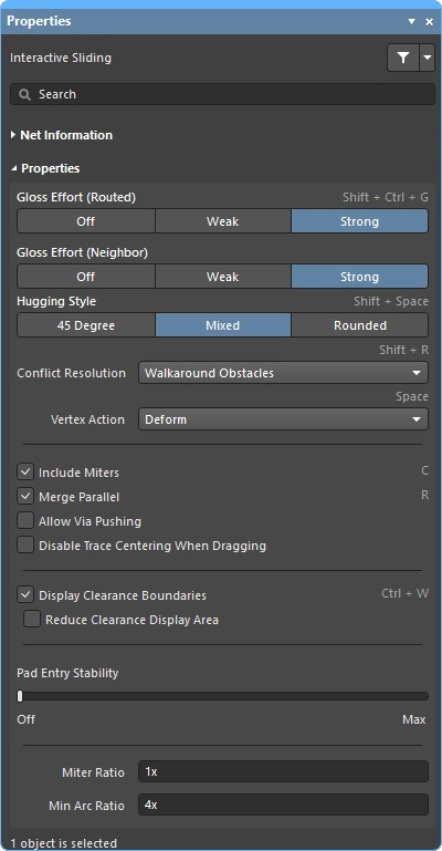 ). During sliding, the interactive routing engine will attempt to maintain the quality of the routing, while complying with the applicable design constraints. Key features that impact on the sliding process include: the routing conflict resolution mode (response to obstacles), the gloss strength (effort in tidying the results), and hugging (how tightly the routes wrap around obstacles and how corners are formed).
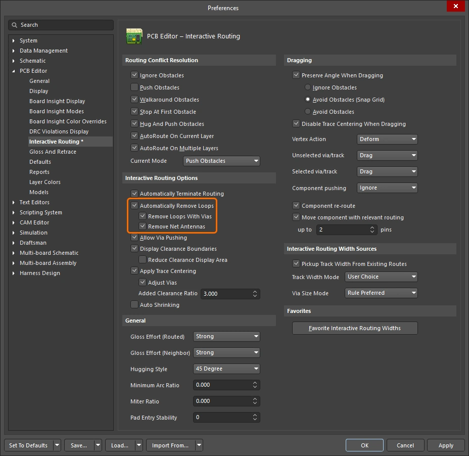
Sometimes it is easier to re-route the path of the differential pair. The interactive routing engine supports this, using a feature called Loop Removal. This feature monitors the interactive routing process, and if it detects that a new path has been routed in parallel to an existing path, it automatically removes the old redundant segments. To re-route the path of a differential pair, select the Route » Interactive Differential Pair Routing command, click anywhere on the existing routing and route the new path, then come back to meet the existing routing where required. The software identifies the loop created between the old path and the new path, when you right-click or press Esc to terminate the route, the redundant segments are automatically removed, including any redundant vias.
Modify the existing differential pair routing using a combination of re-routing and sliding.
Modifying differential pair routing |
|
| Sliding (dragging) the pair | Click and hold on a track segment in one of the pair nets, then move the mouse to start sliding the routing of the pair (
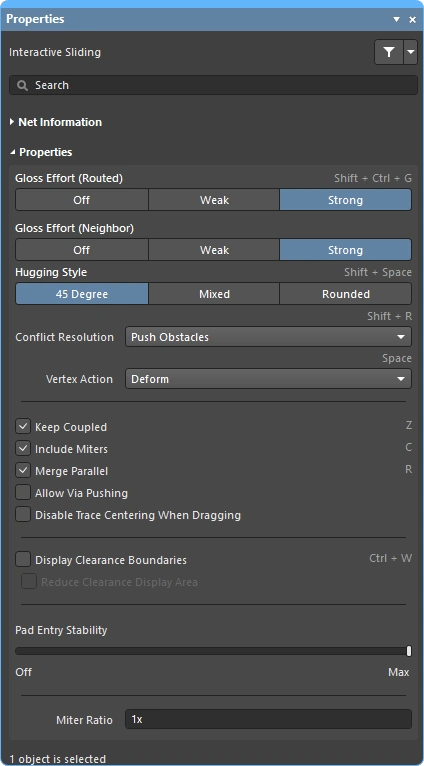
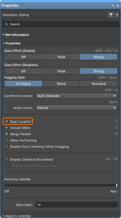
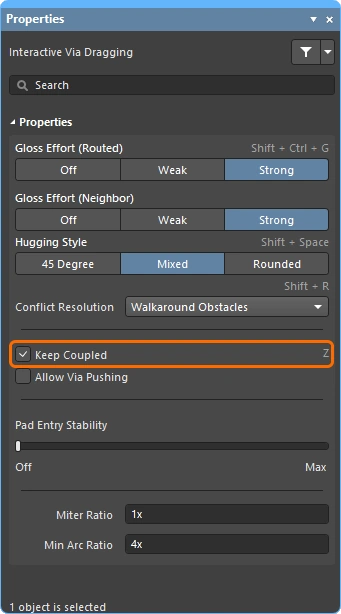
). How the interactive router changes the routing as the cursor moves depends on the current settings of the Properties in the Properties panel ( To recognize the members in a differential pair, the concept of coupling is used. When the software recognizes objects that belong to a differential pair it attempts to drag the pair's partner track or via if the Keep Coupled option is enabled in the Properties panel during interactive sliding ( To confirm that the partner objects are coupled, the software checks that the objects:
|
| What you snap to during sliding | The routing you are sliding will not only snap to the current snap grid, but can also snap other objects depending on: the object snapping settings, the layer snapping setting, and if the snap guides and axes snapping settings are enabled. Press Learn more about cursor-snap behavior. |
| How the sliding routes are glossed | The extent to which the moving tracks are reshaped as you slide them is controlled by the current Gloss Effort (Routed) setting, press the Learn more about the Gloss effort (routed) settings. |
| How the sliding route responds to existing objects | During sliding, one of the Routing Conflict Resolution modes (Ignore, Push, HugNPush) applies ( Learn more about the Conflict resolution mode settings. |
| How neighboring routes are impacted | The impact that the moving tracks have on the adjacent routing is controlled by the current Gloss Effort (Neighbor) setting ( Learn more about the Gloss effort (neighbor) settings. |
| Hugging - how glossing wraps around other objects and forms corners | How the glossing engine wraps the route around other objects and forms the corners is referred to as hugging. The available Hugging Style settings include:
Learn more about the Hugging style settings. |
| Controlling Loop Removal | When you re-route an existing pair, Loop Removal is applied. Loop Removal is on by default ( Learn more about the Loop removal settings. |
| Sliding a route corner | The interactive sliding engine includes algorithms specifically for dragging a vertex (corner).
Learn more about the Vertex action settings. |
 )
) )
) ).
). ).
). )
) )
) )
) ).
).
 )
)Learn more about modifying existing routing.
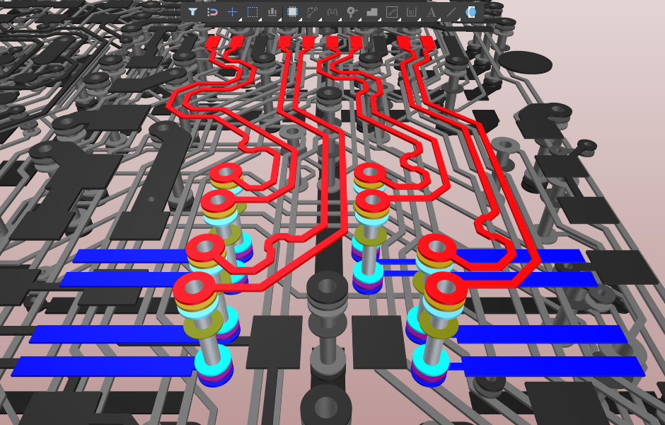
Length Tuning Differential Pairs and Modifying the Accordions
There are two aspects to length tuning differential pairs: tuning the lengths of each pair in a set so that all of the pairs are the same length; and then tuning the length of the shorter net within each pair, a process referred to as phase matching.
To length tune differential pairs, create the following constraints to target the set of differential pairs:
-
A matched length constraint that defines the length matching requirements between pairs. To test the length of one pair against the length of another pair enable the Group Matched Lengths option.
-
A second matched length constraint that defines the within-pair length matching requirements. To test the length of one pair-member against the other pair-member enable the Within Differential Pair Length option in the constraint.
Demonstration of tuning the lengths of the pairs, then tuning the lengths within each pair.
The video shows pair lengths being tuned against other pairs (based on xSignal lengths) by adding length tuning accordions. The shorter member of each pair is then length-tuned against the longer member of that pair. The video then shows how pairs can be moved and reshaped interactively, how a tuning accordion can be deleted, and how a new accordion can be shaped during placement using shortcuts.
Learn more about length tuning differential pairs.