
Simple Placement
At a Glance
- Learn the essential keyboard and mouse actions for selecting, moving, rotating, flipping, and deleting PCB components.
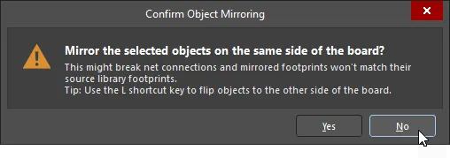
- Understand the difference between flipping a component to the other side of the board and mirroring it on the same side.
- See how connection lines and net line display modes can help you place components more efficiently and with less on screen clutter.
A component can be moved, rotated, and flipped in the PCB design space. To do this, select the required component in the design space by clicking on it. A selected component is highlighted in the current selection color, as shown in the image below.
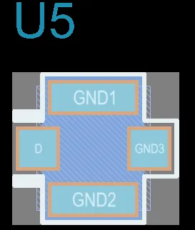 Click once to select a component.
-
Click, hold and drag to move the selected component. The cursor will jump to the component reference point, or the nearest pad center if the Smart Component Snap option is enabled on the PCB Editor - General page of the Preferences dialog. Press the Alt key to constrain the direction of movement to the horizontal or vertical axis depending on the initial direction of movement.
-
While a component is moving on the cursor press the Spacebar to rotate it (Shift+Spacebar to rotate in the other direction). The default rotation step is 90 degrees. To change this setting, use the Rotation Step value in the PCB Editor - General page of the Preferences dialog.
-
While a component is moved on the cursor, press the L key to flip it to the other side of the board.
-
Press Delete to remove the selected component from the PCB.
 ).
).The connection lines are an excellent aid during component placement to help locate and orient components that are connected to each other. As you move the component, connection lines are dynamically optimized so that every connection line follows the shortest path to any other object with the same net name.
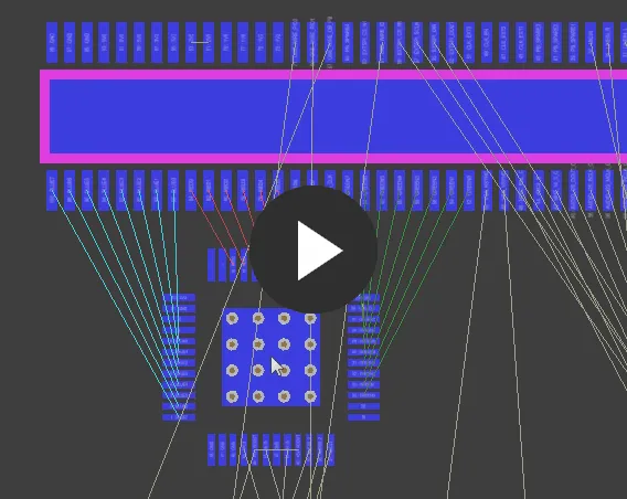
Use the connection lines to help locate and orient the components.
To help reduce visual clutter, as you move a component all connection lines are hidden, except the connection lines connected to that component. Press the N key to cycle through net line connect modes. The following modes are supported:
- Pad to Pad - during the move, connection lines are displayed between pads of the component being moved and the nearest pads of the same nets on the board.
- Breaks - during the move, connection lines are displayed between pads of the component being moved and the track breaks of the same nets on the board.
- Hidden - connection lines are hidden.
Current net line connect mode is shown in the Status Bar and the Heads Up Display.