
Setting Up & Running a DRC
Altium Essentials: PCB Design Rule Checks
This content is part of the official Altium Professional Training Program. For full courses, materials and certification, visit Altium Training.
At a Glance
- Learn how to configure the Design Rule Checker, including selecting rule types and enabling them for Online DRC or Batch DRC.
- Understand the difference between Online DRC and Batch DRC, when to use each one, and what is required for them to function properly.
- Find out where violations appear, how reports are generated, and how to investigate issues directly in the PCB design space.
Checking that the objects in the design space comply with the design requirements, or rules, is performed by the Design Rule Checker.
Configuring the Design Rule Checker
Design Rule Checking is configured in the Design Rule Checker dialog (Tools » Design Rule Check). The dialog includes a selection tree on the left where you choose what to configure. As you choose, the right-side of the dialog changes to suit your selection.
To configure what design rules are checked, select the Rules to Check section in the dialog, as shown below. The right side of the dialog will list all of the design rule types that can be checked. Note that for each design rule-type, there are separate checkboxes to enable/disable Online DRC and Batch DRC.
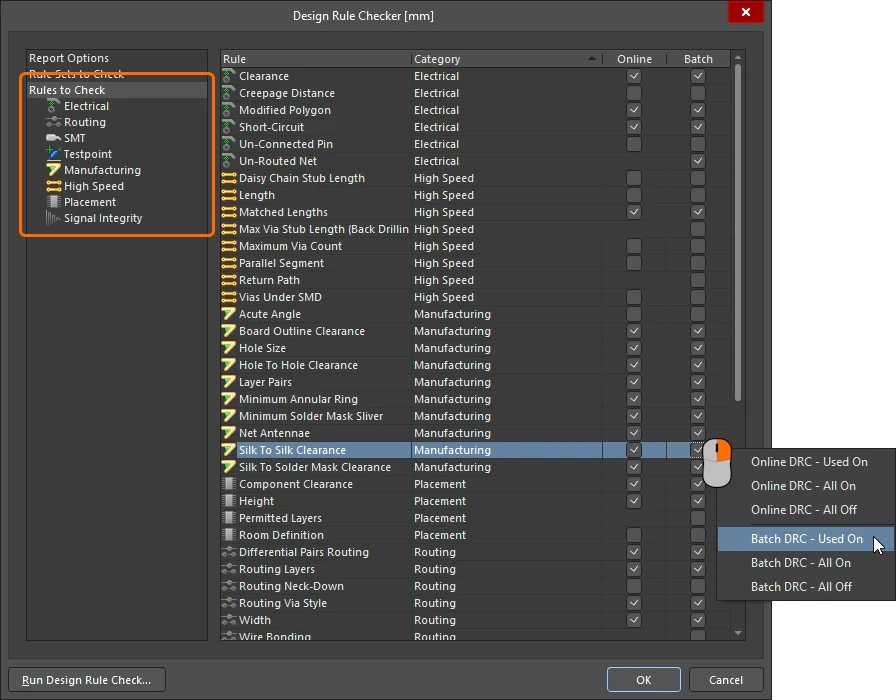
Configuring which Rules are Checked |
|
| Working with all rule types | Click on Rules to Check in the tree on the left to display all available design rule types. To sort the contents on the right side of the dialog based on one of the headings, click the relevant heading. For example Category has been clicked in the image above. |
| Working with a rule class | To focus on a specific class of rules, such as Electrical or Routing, select that rule class in the tree on the left. |
| Enabling a specific rule type | Click on the checkbox to enable a specific rule type for Online and/or Batch design rule checking. |
| Enabling multiple rule types | Use the right-click context menu to enable or disable the setting for multiple rules: Used On – enable checking if a rule of that type has been defined for this board All On – enable checking of all rule types All Off – disable checking of all rule types |
| Run a DRC | Click the Run Design Rule Check button to check all of the rules that currently have the Batch checkbox enabled, in accordance with the settings configured in the Report Options page of the dialog. More about performing a batch DRC. |
| What next? | There are multiple ways of finding, identifying and resolving design rule violations, these are detailed in the Interrogating & Resolving Design Rule violations page. |
Enabling Online DRC
Online Design Rule Checking runs in the background, in real-time, flagging and/or automatically preventing design rule violations. This is especially helpful when interactively routing your board as it will immediately highlight violations, such as clearance, width and parallel segment violations.
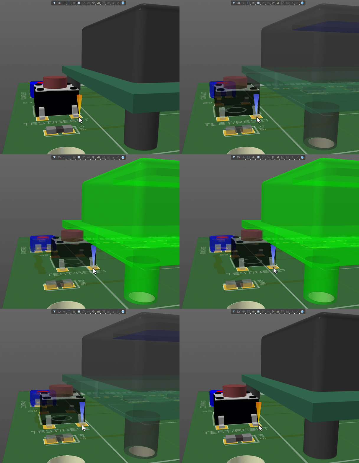
Online DRC flags violations as soon as they happen.
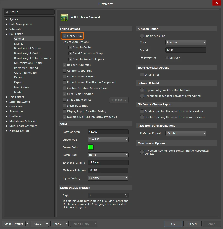
For a rule to be subject to Online DRC, the following three requirements must be met:
-
The Online DRC feature must be enabled in the PCB Editor - General page of the Preferences dialog (
 )
)
-
The rule must be enabled for the design rules system to be aware of it. This can be done in either the PCB Rules and Constraints Editor dialog or the PCB Rules and Violations panel, by ensuring the Enabled option for that rule is checked (
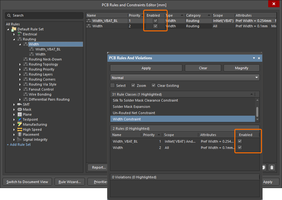 ).
).
-
The rule type must be enabled for online checking in the Design Rule Checker dialog (
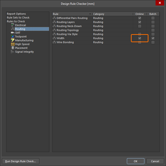 ).
).
If any objects are found to be in violation of an applicable design rule that is enabled for online checking, they are highlighted in the design space in accordance with the currently defined violation display options.
Setting up and Performing a Batch DRC
Online DRC detects new violations as you work, while Batch DRC allows a check to be manually run at any time during the board design process. So, while good designers know the value of the Online DRC, they also know that board design should always end with a Batch DRC.
A batch-mode DRC is initiated by clicking the Run Design Rule Check button at the bottom-left of the Design Rule Checker dialog, testing all rules currently enabled in the Batch column of the Rules to Check section of the dialog. If the Create Report File option is enabled in the first page of the dialog, a report will be created and opened (in accordance with the report format options). The report lists each rule that was tested, rules that are not present in the design are not tested. After a Batch DRC has completed, all detected violations are also listed as messages in the Messages panel.
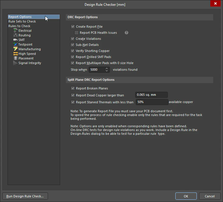
Configure the reporting options for a Batch Design Rule Check.
DRC Report Options |
|
| Run a Batch Design Rule Check | Run the Tools » Design Rule Check command to open the Design Rule Checker dialog. Click the Run Design Rule Check button to perform a Batch DRC, in accordance with rules enabled for Batch checking and additional options defined for this type of checking. |
| Create Report File | If enabled, a report is generated after running a Batch DRC for the board. The default report format is HTML, which is named Design Rule Check - <PCBDocumentName>.html. The report format and default opening behavior is configured in the PCB Editor – Reports page of the Preferences dialog. More about the DRC report format options. |
| ↳ Report PCB Health Issues | The PCB Health Check Monitor is a feature that detects potential design flaws that might not actually be design violations that fail DRC. Health check options are configured in the Properties panel ( |
| Create Violations | When enabled, violations are highlighted in the design space in accordance with the current violation display options settings. This option is also required to have violations appear listed in the Violations region of the PCB Rules And Violations panel. |
| Sub-net Details | If an Un-Routed Net rule has been defined, enable this option to include sub-net details in the DRC report. |
| Verify Shorting Copper | Net Tie components are created to allow two nets to be connected to each other in a controlled manner, for example AGND and DGND. This option verifies the integrity of the shorting copper in the Net Tie components used in the design, looking for any unconnected copper in the component (indicative of a pad not shorting the other pad(s) correctly). Learn more about intentionally connecting two nets. |
| Report Drilled SMT Pads | Enable this option to report any SMT (Surface Mount Technology) pads that have been erroneously drilled. |
| Report Multilayer Pads with 0 size Hole | Detect multi-layer pads that have a hole size of zero (essentially making it an surface mount pad). |
| Stop when <n> violations found | Define the maximum number of violations that can be detected before the batch DRC process is stopped (default = 500). Limiting the number of violations that are reported can help keep the checking process manageable. |
| Report Broken Planes | Broken planes occur when an area of a plane connected to a net becomes electrically disconnected from the rest of the plane. An example of where this may occur is a connector is placed across a region of a split plane, but is not connected to that plane. If the clearance voids around the pins join to completely cut through the plane copper, they can then effectively break that split plane into two parts. |
| Report Dead Copper larger than | Dead copper refers to sections of copper in a polygon object that have no connectivity to the net assigned to that polygon, and which also become electrically disconnected from the original parent plane. An example of where this may occur is a connector (not connected to the plane) with closely spaced pins, in which the voids around the pins join to isolate areas of plane copper from the rest of the plane. Use the associated field to specify a value for the maximum permissible area of dead copper, beyond which is considered a rule breach (default = For objects that have no net assigned |
| Report Starved Thermals with less than n% available copper | Enable this option to have the batch rule checking process look for and report 'starved' thermal connections larger than the specified percentage. Thermals are connections to a plane with thermal relief 'cutouts' around them to reduce heat conductivity to the plane copper. A thermal can become 'starved' when the surface area of the copper spokes connecting it to the plane is reduced by void areas. This option also checks the surface area for the thermal (not just the spokes) against any void areas that encroach into the thermal. Use the associated field to specify a value for the minimum permissible percentage of connecting copper that must remain, below which is considered a rule breach (default = 50%). |
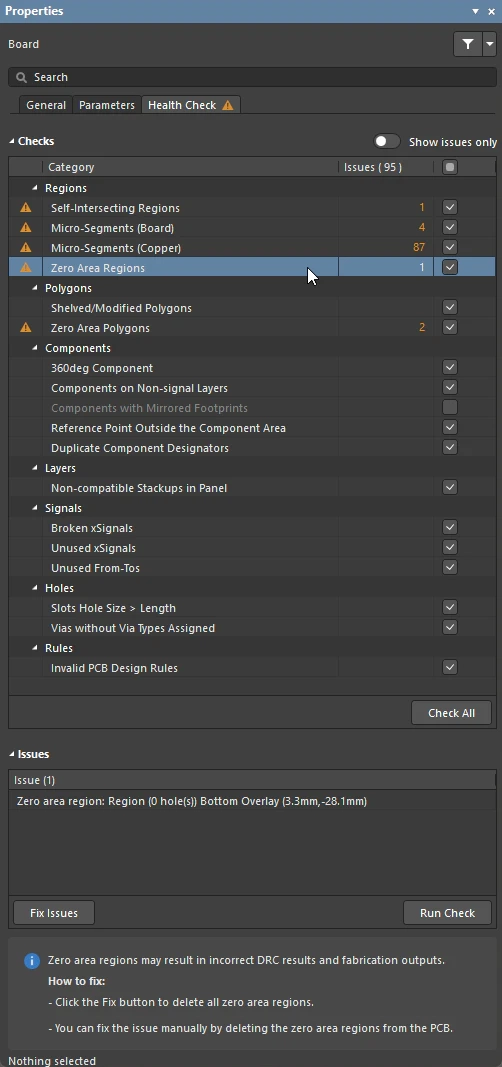 ).
).Setting up the DRC Report
A Design Rule Verification Report is generated as part of a Batch Design Rule Check (DRC), if the Create Report File option is enabled in the Design Rule Checker dialog. The report format and auto-opening options are configured in the PCB Editor - Reports page of the Preferences dialog.
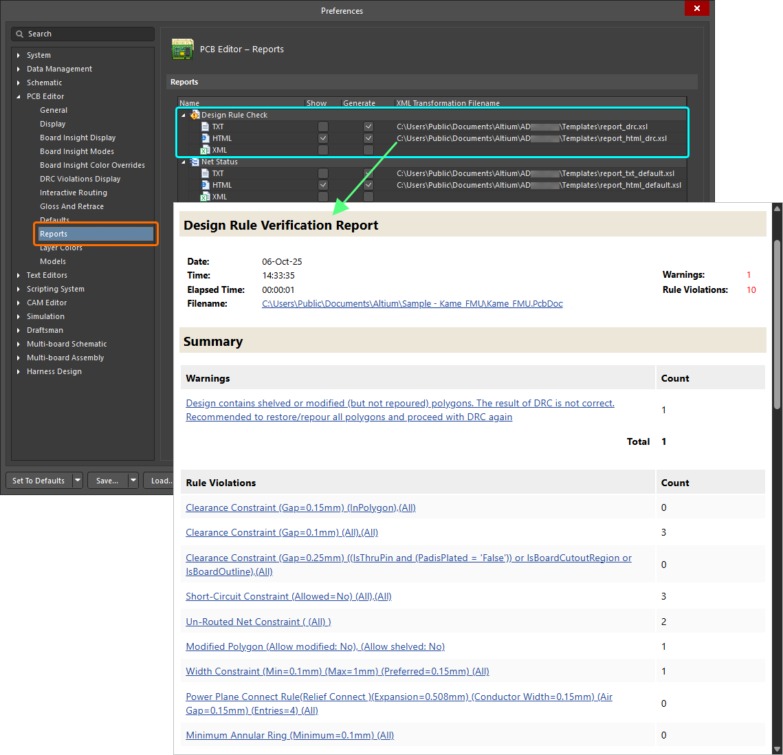
Generate a DRC report as part of the Batch DRC process.
Supported formats are:
-
TXT – generates the file Design Rule Check - <PCBDocumentName>.drc.
-
HTML – generates the file Design Rule Check - <PCBDocumentName>.html.
-
XML – generates the file <PCBDocumentName>.xml.
Configuring the Display of DRC Violations
Design violations can be graphically marked in the design space using an overlay, and/or a detail marker. Both styles of DRC markers, the violation overlay and the violation detail markers, are configured in the PCB Editor – DRC Violations Display page of the Preferences dialog. Each of the styles has its own advantages:
-
The overlay style applies a colored overlay to the entire violating object, in one of four styles. How they appear as you zoom in and out is controlled by the Overlay Zoom Out Behavior option. The Override Color Dominates style is excellent for spotting a violation when zoomed out.
-
Instead of highlighting the entire violating object, detail markers are designed to give feedback on the type of violation.
The lower section of the dialog page is used to enable which violations should be flagged, or marked. Note that these checkboxes only control the display of detected violations, even when a rule-type is disabled here the design rule checker will still detect all violations of that type if, there is a rule defined, and that rule-type is enabled for checking.
Violation Display Preferences
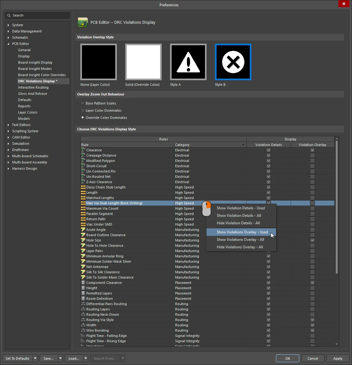
Control over how the DRC violations are displayed and which violation types are to be flagged is configured in the PCB Editor – DRC Violations Display page of the Preferences dialog.
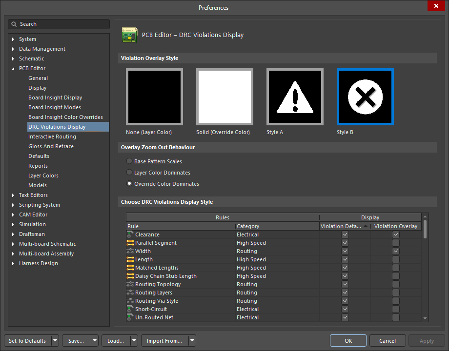
Choose how you want DRC violations to be displayed in the design space - using custom graphics and/or a defined violation overlay.
DRC Violations Display |
|
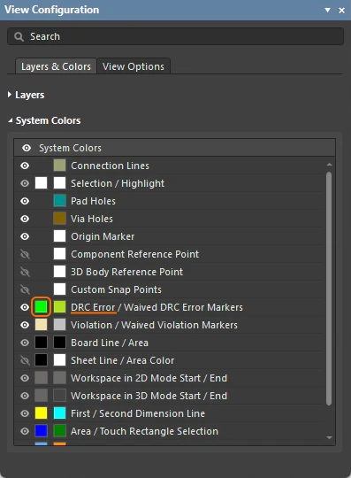
| Violation Overlay Style | The violation overlay is drawn over the violating design primitives. Select the visual overlay style to specify how violations appear in the PCB design space. The override color used to highlight objects in violation is the DRC Error Markers system color, configured in the System Colors region of the Layers and Colors tab of the View Configuration panel (
|
| Overlay Zoom Out Behavior | This option determines how the Style A or B violation overlays are displayed as you zoom out:
|
| Choose DRC Violations Display Style | Use the grid region to choose the display style used on a per-rule type basis.
|
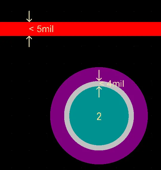
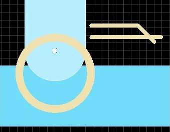
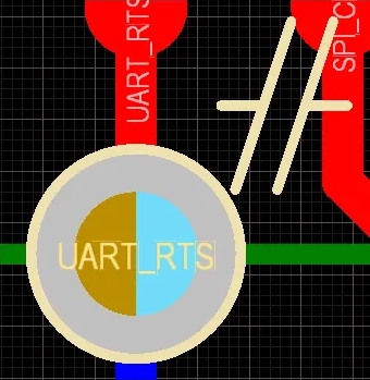
| Violation Detail Markers | Most design rules that can be included in either Online and/or Batch design rule checking have an associated detail violation graphic – appearing within the design space when a particular rule is violated, on the layer(s) involved with that violation. In some cases, the graphic shows not only where the violation is occurring, but also why – displaying the constraint value defined for the rule and indicating how the offending primitive(s) are either below or above this value, for example a Width or Minimum Annular Ring violation ( The graphic for other detail markers, including those used to represent violations of Net Antennae ( |
| Color of the DRC markers | The colors of both types of markers are configured in the System Colors region of the Layers and Colors tab of the View Configuration panel ( |
| Other dialog options | The Defaults, Save, Load and Import From buttons are for managing the Altium Designer preferences (the preferences saved with this installation of Altium Designer). To reset the PCB Editor – DRC Violation Display page of preferences to default, click the down-arrow on the Set to Defaults button and select Default (Page) from the menu (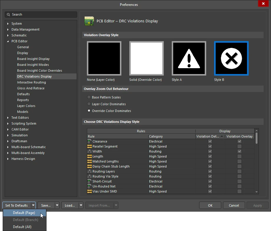 ). Learn more about Accessing, Defining & Managing System Preferences. ). Learn more about Accessing, Defining & Managing System Preferences. |
 ).
). ).
). ).
). ).
). ).
). ).
). ).
). )
) )
) )
)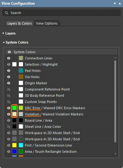 ).
). )
)Configuring Force Batch Check for Rule Sets
The PCB editor's rule system includes the ability to define design rules in rule sets. Rule sets allow the designer to group and reuse a set of design rules specific to, for example, an interface, or a manufacturer. The rules system automatically analyzes all rules in all of the rule sets to identify the applicable design rule.
In addition to this, the designer has the option to force a check of one or more of the rule sets during batch DRC, testing the rules in those set(s) in addition to the rules checked during normal DRC.
For example, if a net is scoped by a Width rule in the Default Rule Set and a Width rule in a user-created rule set, this net will be additionally checked against the Width rule from the user-created rule set if the Force Batch Check option is enabled for this rule set, even if this rule has a lower priority than the Width rule from the Default Rule Set. Entries for detected violations of design rules that are included in force-checked rule sets are labeled Force Checked <RuleSetName> in the DRC report, the Messages panel, and the PCB Rules And Violations panel.
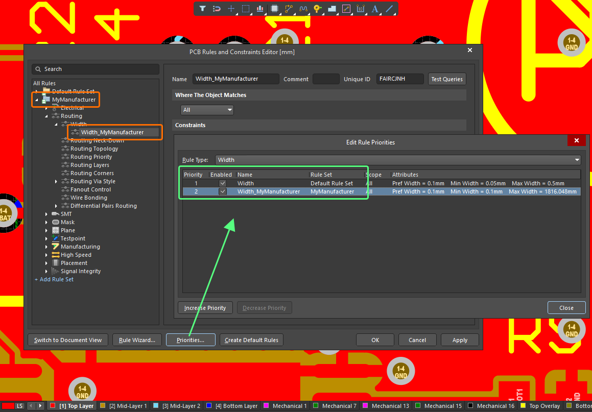
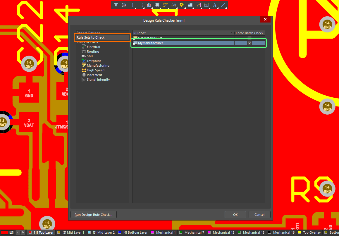
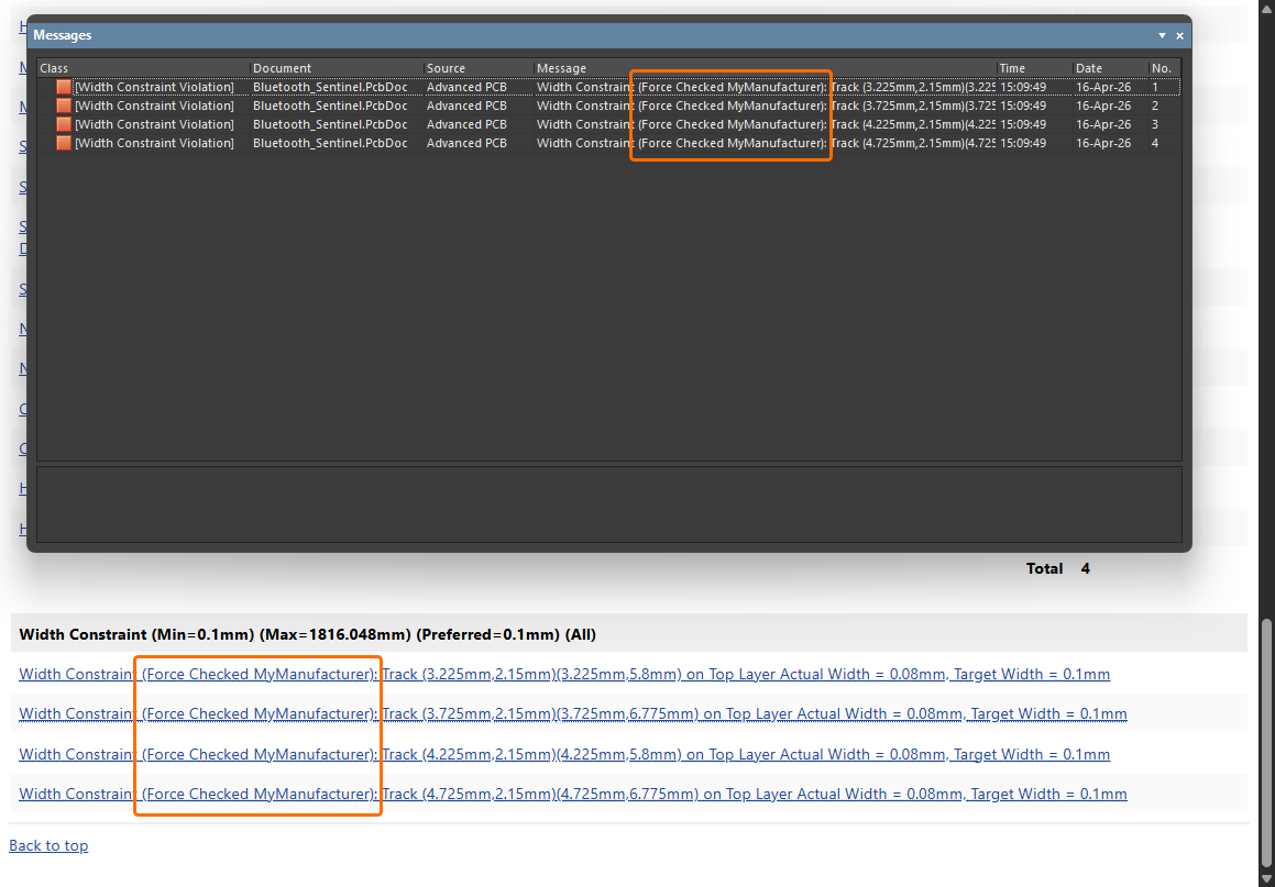
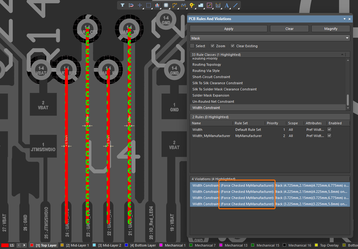
Force Checking Rule Sets |
|
| What are Rule Sets? | The PCB editor's rule system includes the ability to define design rules in rule sets. Rule sets allow the designer to group and reuse a set of design rules specific to, for example, an interface, or a manufacturer. The rules system automatically checks across all rule sets and identifies the highest priority rule of each rule type, to use for online and batch DRC. |
| What does Force Checking mean? | When the Force Batch Check option is enabled for a rule set, not only is the applicable rule of the highest priority for each rule type checked, but also the applicable rule of the highest priority for each rule type, within this rule set, is force-checked during Batch DRC. Essentially, force-checking runs in parallel to normal batch DRC, executing an additional DRC run for each rule set included for force checking ( Note that Force Batch DRC(s) are performed after 'normal' DRC of applicable rules. If a number of violations detected during the 'normal' DRC reaches the number specified in the Stop when n violations found option on the Report Options page of the Design Rule Checker dialog, the DRC will stop, and Force Batch DRC will not start. |
| Enabling Force Check | Use the options in the Rule Set to Check page of the Design Rule Checker dialog to enable a force check of a specific rule set ( |
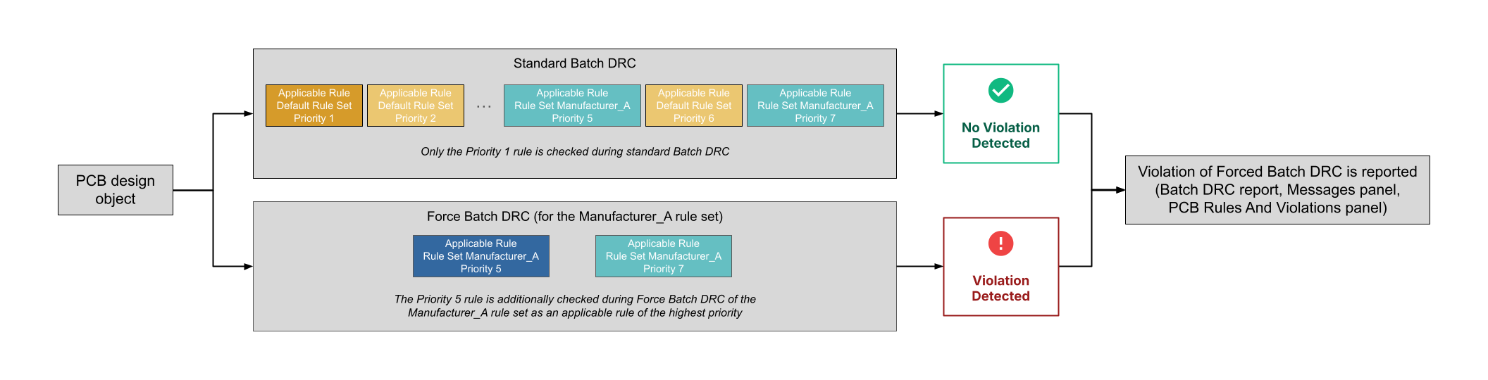 ).
).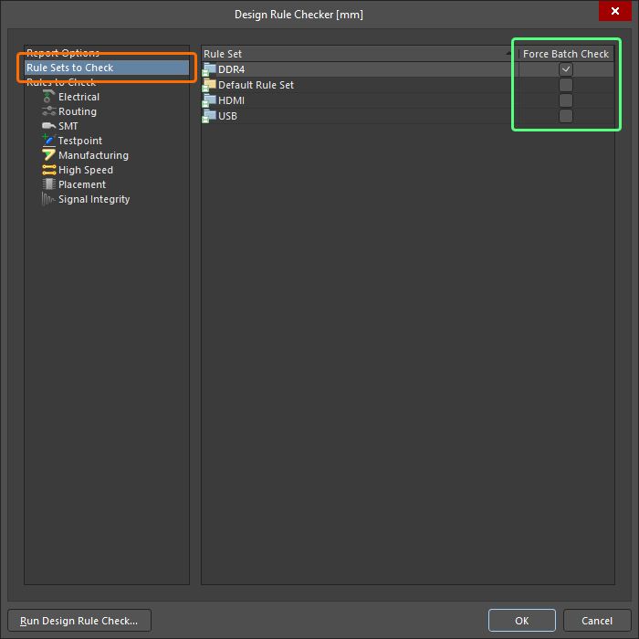 ).
).Refer to the Defining, Scoping & Managing PCB Design Rules page to learn more about rule sets.