Library Browsing
The panel has three main sections, each offering a different scope or view of the footprints in the active PCB Library:
- Footprints - a list of footprints in the active library. The number of pads and primitive objects used to define the footprint is listed for each entry.
- Footprint Primitives - the primitive objects and their main properties that make up the currently selected footprint.
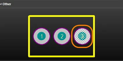
- Other - a simplified, overall view of the currently selected footprint with the main editor view indicated by an overlay graphic.
As a footprint is selected in the panel, its constituent primitives populate the Footprint Primitives section and the footprint is displayed in the main editor design space. Selecting a primitive object in the panel causes the corresponding object to be highlighted in the editor design space. In this way, the PCB Library panel offers a fast and easy way to browse, view and access PCB library footprints.

Double-clicking on a Footprint entry opens the PCB Library Footprint dialog, and double-clicking on a Footprint Primitives entry will access its corresponding Properties panel - see more options in the Right-Click Menus section below.
Filtering Content
The contents of the list can be filtered, enabling you to quickly find a particular footprint within the library. This is especially useful if the library contains a large number of items. Filtering can be applied using the following methods:
Indirect Filtering
This method uses the Mask field at the top of the panel to filter the contents of the list. Masking is applied based on the entry in the field. Only those footprints in the list targeted by the scope of the entry will remain displayed.

Note that the Mask field is not case sensitive. To list all footprints again, clear (delete) the entry in the Mask field.
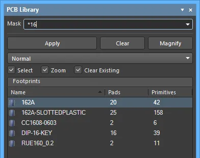
Use the * wild card operator for more elaborate filtering. For example, typing m* will display only footprints whose names begin with m, or as in the image below, typing *16 will display only footprints that contains 16 in the name.
Direct Filtering
This method is available for all list regions in the panel and allows you to quickly jump to an entry by directly typing within the area of the list. Masking is not applied, leaving the full content of the list visible at all times.
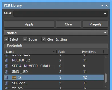
To use the feature to quickly find a footprint, click inside the Footprints section of the panel then type the first letter of the footprint to which you want to jumps. For example, if you wanted to quickly jump to footprint entries starting with the letter S, you would press "S" on the keyboard. The first footprint in the list starting with S will be made active, and the letter will be highlighted to indicate that filtering of the list is based upon it.
If there are multiple footprints starting with the same letter and especially if the library is particularly large, type additional letters to target the specific entry you require, for example, "SO" as shown below.
To clear the current filtering allowing you to enter a different starting letter, press Esc. Use the Backspace key to clear the previously entered filter characters in sequence.
Combination Filtering
In some situations, it may be helpful to use Indirect and Direct filtering together. If, for example, you recall that the footprint you want to locate has a sub-type number of 4 and a prefix of PO, this information can be used as Indirect (Mask) and Direct entries.
Footprints Controls
- Place - click to place the selected footprint.
- Add - click to add a new footprint to the list. The default name will be
PCBCOMPONENT_1.
- Delete - click to delete the selected footprint. A dialog will open asking for confirmation before the delete occurs.
- Edit - click to open the PCB Library Footprint dialog to edit the selected footprint.
Browsing Footprint Primitives
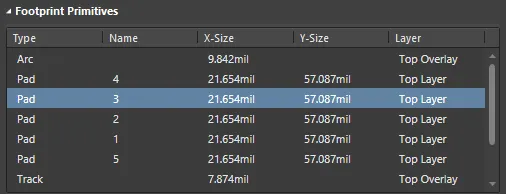
The Footprint Primitives section lists all primitive objects that constitute the footprint currently selected in the Footprints list. For each primitive entry, the following information is displayed:
- Type - the type of primitive object (e.g., pad, track, arc, etc.).
- Name - the specified value for the objects' designator (where one exists).
- X-Size - the X dimension of the object (e.g., the width of an arc, track or fill, the X-Size value of a pad).
- Y-Size - the Y dimension of the object (e.g., the height of a fill, the Y-Size value of a pad). This field will be empty for a track or arc.
- Layer - the layer upon which the object resides.
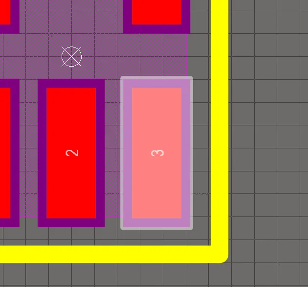
As individual object primitives are selected in the panel, the matching object (track, arc, pad, etc.,) is graphically highlighted in the editor design space.
Controlling the Display of Browsed Entries in the Design Space
Selecting an entry in either panel list region applies a filter, essentially using the entry as its scope. The visual result of the applied filtering on the document in the design editor window is determined by a series of highlighting controls located at the top of the panel.
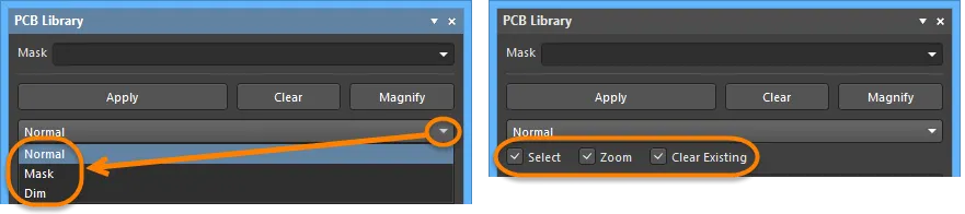
- Mask / Dim / Normal - provides the options for visibly contrasting filtered and unfiltered objects within the design editor window. The effectiveness of masking and dimming is determined by the Highlighting Options set in the PCB Editor - Display page of the Preferences dialog.
- When Mask is selected, filtered objects will appear visible in the design editor window, with all other objects being made monochrome. When this option is applied, unfiltered objects will be unavailable for selection or editing.
- When Dim is selected, filtered objects will appear visible in the design editor window, with all other objects retaining their colors but shaded.
- Select - when enabled (default), the filtered objects will be selected in the design space.
- Zoom - when enabled (default), the filtered objects will be zoomed and centered (where possible) in the design space.
- Clear Existing - when enabled (default), an existing filter will be cleared before applying a new one. Disabling this option allows you to extend an existing filter, essentially refining the filter further by applying a new filter in addition to the existing one.
Any combination of these options can be enabled. For example, you might want to have all filtered objects zoomed, centered and selected in the design space as well as applying masking to take away the clutter of other design objects. Use the Clear button to clear the currently-applied filter. All objects in the design space will become fully visible and available for selection/editing. If you want to re-apply the filter, click the Apply button.
Using the Panel's Mini-viewer
The bottom section provides a mini-viewer for the document, with an image of the active footprint central to its window. The area currently displayed in the design editor window is denoted by white hash marks as highlighted in the following image.
Click the Magnify button at the top of the panel to provide a floating magnifying glass and zoom cursor in the design editor window. As you move these around in the design space, the mini-viewer in the panel will contain the magnified image of the active footprint centered on the cursor. This allows you to browse the document at full size in the design editor window, while looking at zoomed detail in the mini-viewer window.
Use the Page Up and Page Down keys to increase or decrease the magnification. Right-click, click or press Esc to exit magnify mode.
Right-click Menus
Footprints
- New Blank Footprint - select to add a new footprint to the list. The footprint is given the default name PCBCOMPONENT_1 and a blank sheet is opened in the design editor window, ready for you to start placing the primitive objects that will define it.
- Footprint Wizard - click to open the Footprint Wizard. The pages of the Wizard will guide you through the steps to creating a new component footprint.
- Cut - place a copy of the selected footprint(s) onto the PCB Library Editor's internal clipboard then permanently delete the footprint(s) from the library. A confirmation dialog will appear asking for verification to proceed with the deletion.
- Copy - place a copy of the selected footprint(s) onto the PCB Library Editor's internal clipboard.
- Copy Name - copy the name of the focused footprint to the PCB Library Editor's internal clipboard.
- Paste - paste a footprint from the PCB Library Editor's internal clipboard into the active library document. The entry for this command will change to reflect how many valid footprints are on the clipboard.
- Delete - permanently delete the selected footprint(s) from the library document. A confirmation dialog will appear asking for verification of whether or not to proceed with the deletion.
- Select All - quickly select all footprint entries in the list.
- Footprint Properties - click to access the PCB Library Footprint dialog in which you can view/modify the Name, Height, Description, and Type for the focused footprint. The PCB Library Footprint dialog will also open when a footprint entry is double-clicked in the panel.
- Place - place the focused footprint onto the PCB design document. When clicked, the last PCB to have been active (regardless of the project to which it belongs) will be made the active document in the design space.
- Update PCB With <FocusedFootprint> - pass on changes made to the focused footprint within the library document to all open PCB design documents where that footprint has been placed. All instances of the footprint will be updated.
- Update PCB With All - pass on all changes made to footprints within the library document to all open PCB design documents where these footprints have been placed. All placed instances of a changed footprint will be updated.
- Report - generate a report for the active footprint. After launching the command, the report will be generated (
LibraryName.CMP) in the same folder as the source PCB library document and will automatically be opened as the active document in the design editor window. The report lists information including footprint dimensions, a breakdown of the primitive objects that constitute the footprint, and the layers on which they reside.
- Delete All Grids And Guides In Library - click to delete grids and guides for this library.
Footprint Primitives
- Show Pads - enable to display pad entries.
- Show Vias - enable to display via entries.
- Show Tracks - enable to display track entries.
- Show Arcs - enable to display arc entries.
- Show Regions - enable to display region entries.
- Show Component Bodies - enable to display component body entries.
- Show Fills - enable to display fill entries.
- Show Strings All - enable to display string entries.
The above listed commands will depend on the types of objects in the selected document. Other Show commands may also be available.
- Select All - quickly select all footprint primitive entries in the list.
- Report - generate a primitive information report for the focused footprint in the Footprints section of the panel. After launching the command, the Report Preview dialog will open containing the primitive information currently displayed in the Footprint Primitives region of the panel. Use the dialog to view, print and export the report in various file formats.
- Properties - access the corresponding Properties panel for the focused primitive in which you can view and modify properties as required. The primitive's corresponding Properties panel also will open when a primitive entry is double-clicked in the panel.
Notes
- Standard Ctrl+Click and Shift+Click functionality is supported for selection of multiple entries in a list.
- The active footprint is that whose graphics are currently displayed in the design editor window. A footprint can be active without necessarily being selected and/or focused in the Footprints list.
- Ctrl+Click over a selected entry in a list to deselect it. If the entry is the only one selected for that section, performing this action will clear the filter.
- The keyboard shortcuts Up Arrow, Home, End, and Down Arrow can be used to display the previous, first, last, and next footprint, respectively.
- In regions of the panel where multiple columns of data exist, the data may be sorted by any column by clicking on the header for that column. Clicking once will sort in ascending order; click again to sort by descending order.
- You can change the order in which columns of data are displayed. To move a column, click on its header and drag it horizontally to the required position. A valid position is indicated by the appearance of two positional arrows.
- The filtering applied when browsing design objects is permanent. If the Mask or Dim highlight method has been selected, all objects not falling under the scope of the filter will become faded (depending on settings) in the design space and are not available for selection or editing. Clicking inside the design editor window will not clear the filter. A permanent filter must be cleared by clicking on the Clear button from within the panel.
- The footprint that you paste into the active library document can originate from either a PCB design document or another PCB library document.
- If multiple footprints have been copied to the clipboard from the main design in the PCB Editor, only the last footprint of the group to have been selected will be pasted into the library document.
- If the same footprint is pasted into the library more than once or if more than one new footprint is added to the library without renaming, the copies are distinguished by the suffix - DUPLICATE, - DUPLICATE1, - DUPLICATE2, etc.
- A PCB design document must be open before a library footprint can be placed using the Place command.
- A PCB design document must be open in order to pass on changes made to footprints in the library document.
- When a new PCB library document is created the panel will, by default, contain a single, blank footprint -
PCBCOMPONENT_1.
- Library footprints can be edited only in the source PCB library (
*.PcbLib). You cannot edit the footprints in an integrated library (*.IntLib). You would have to de-compile the integrated library first then edit the required footprint(s) in the source PCB library document(s). The source can then be recompiled to produce the updated integrated library.
