Capacitors

Use the drop-down to select the type of capacitor you want to design. Choose from Through Hole or Surface Mount.

To change the pads' dimensions, click on the values and enter the new values.
This page will have a slightly different look if Surface Mount was selected, however, its functionality is the same.
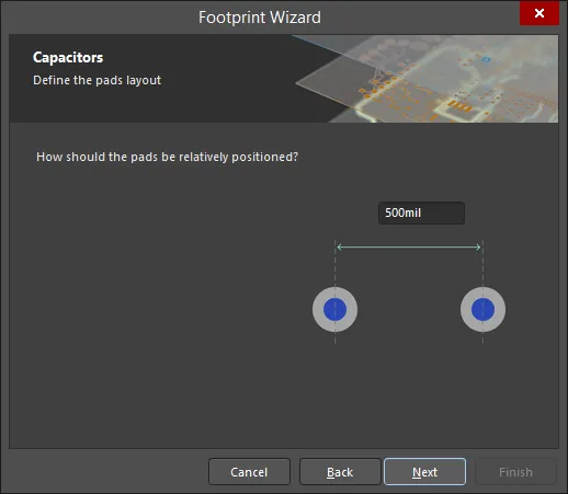
To change the pads positioning, click on the value and enter the new value.
This page will have a slightly different look if Surface Mount was selected, however, its functionality is the same.

This page appears if Through Hole was selected. If Surface Mount was selected, the page below appears.
Use the drop-down to select the capacitor's polarity, either Not Polarised or Polarised. Use the drop-down to select the capacitor's mounting style, either Axial or Radial.

This page appears if Surface Mount was selected.
Use the drop-down to select outline type, either Non polarised Outline or Polarised Outline.

To change the outline dimensions, click on the values and enter the new values.
This page will have a slightly different look if Surface Mount was selected, however, its functionality is the same.
