 Altium Designer 文档
Retired Documentation No Longer Applicable to a Later Version of Altium Designer
Retired Documentation - Design Rules
Altium Designer 文档
Retired Documentation No Longer Applicable to a Later Version of Altium Designer
Retired Documentation - Design Rules
Working with the Clearance Design Rule on a PCB in Altium Designer
Rule category: Electrical
Rule classification: Binary
Summary
This rule defines the minimum clearance allowed between any two primitive objects on a copper layer. Either a single value for clearance can be specified, or different clearances for different object pairings, through use of a dedicated Minimum Clearance Matrix. The latter, in combination with rule-scoping, provides the flexibility to build a concise and targeted set of clearance rules to meet even the most stringent of clearance needs.
Constraints
 Default constraints for the Clearance rule. Roll the mouse over the image to compare the two modes available.
The rule scope returns a set of objects, the constraints detailed below are then applied to that set of objects:
- Connective Checking - the set of net objects returned by the rule scope can then be further narrowed down in the following ways:
Different Nets Only- constraint is applied between any two primitive objects belonging to different nets (e.g. two tracks on two different nets).Same Net Only- constraint is applied between any two primitive objects belonging to the same net (eg, between a via and pad on the same net, or two track segments in the same net).Any Net- constraint is applied between any two primitive objects belonging to any net in the design. This is the most comprehensive of the three options and covers the possibility of the objects belonging to the same net, or different nets.- Different Differential Pair - constraint is applied between any two primitive objects belonging to different nets of different differential pairs (e.g. a track in DiffPair1 and a track in DiffPair2). The rule does not apply between primitives in the two nets in the same differential pair (eg, DiffPair1_P and DiffPair1_N). Use this constraint to configure the clearance between the differential pairs.
- Same Differential Pair - constraint is applied between any two primitive objects belonging to the different nets in the same differential pair (e.g. a track in TX_P and a track in TX_N). Use this constraint to configure the clearance when the nets in the differential pair must be closer together than allowed by the general clearance.
► Learn more about Differential Pair Clearance Checking
- Ignore Pad to Pad Clearances within a footprint - toggle this option on/off to specify whether clearances between pads in the same component footprint are ignored. This option is disabled by default.
- Minimum Clearance - the value for the minimum clearance required. A value entered here will be replicated across all cells in the Minimum Clearance Matrix. Conversely, when a different clearance value is entered for one or more object pairings in the matrix, the Minimum Clearance constraint will change to N/A, to reflect that a single clearance value is not being applied across the board.
- Minimum Clearance Matrix - provides the ability to fine-tune clearances between the various object-to-object clearance combinations in the design.
Working with the Clearance Matrix
For many users, there is no great difference between Track and Arc primitives. And when it comes to Fill, Region, and Polygon objects, most users just see these as more 'copper.' With this in mind, the minimum clearance matrix for the Clearance rule has been enhanced to operate in two modes:
- Simple - in this mode, Track and Arc objects (including Track Keepout and Arc Keepout objects) are combined into the single Track entry. Fill, Poly, and Region objects (including Fill Keepout and Region Keepout objects) are combined into the single Copper entry. The Simple mode is the default mode, regardless of whether opening an existing design or a new design.
- Advanced - this mode is the traditional matrix, present in previous versions of the software, with all objects presented.
Definition of clearance values in the matrix can be performed in the following ways:
- Single cell editing - to change the minimum clearance for a specific object pairing. Simply click on a cell to select it for editing.
- Multi-cell editing - to change the minimum clearance for multiple object pairings:
- Use Ctrl+Click, Shift+Click, and Click+Drag to select multiple cells in a column.
- Use Shift+Click, and Click+Drag to select multiple contiguous cells in a row.
- Use Click+Drag to select multiple contiguous cells across multiple rows and columns
- Click on a row header to quickly select all cells in that row.
- Click on a column header to quickly select all cells in that column.
With the required selection made (either a single cell or multiple cells), making a change to the current value is simply a case of typing the new value required. To submit the newly entered value, either click away on another cell, or press Enter. All cells in the selection will be updated with the new value.
![]() Example multi-cell editing. Notice that as different values for clearance now exist for one or more object pairings, the Minimum Clearance constraint has
Example multi-cell editing. Notice that as different values for clearance now exist for one or more object pairings, the Minimum Clearance constraint has
changed to N/A, to reflect that a single clearance value is no longer being applied for all object-to-object clearance combinations.
Hole-to-Object Clearance Checking
Designers can check clearances between the edges of drill holes and neighboring copper objects on signal layers. This is particularly beneficial in preventing the routing of track too near to a drilled hole, which could otherwise suffer from any potential wandering of the drill during board fabrication. The row at the bottom of the Clearance rule's minimum clearance matrix is used to define the desired clearances.

Set clearance values to catch any copper objects that are too close to the edges of drill holes in the design.
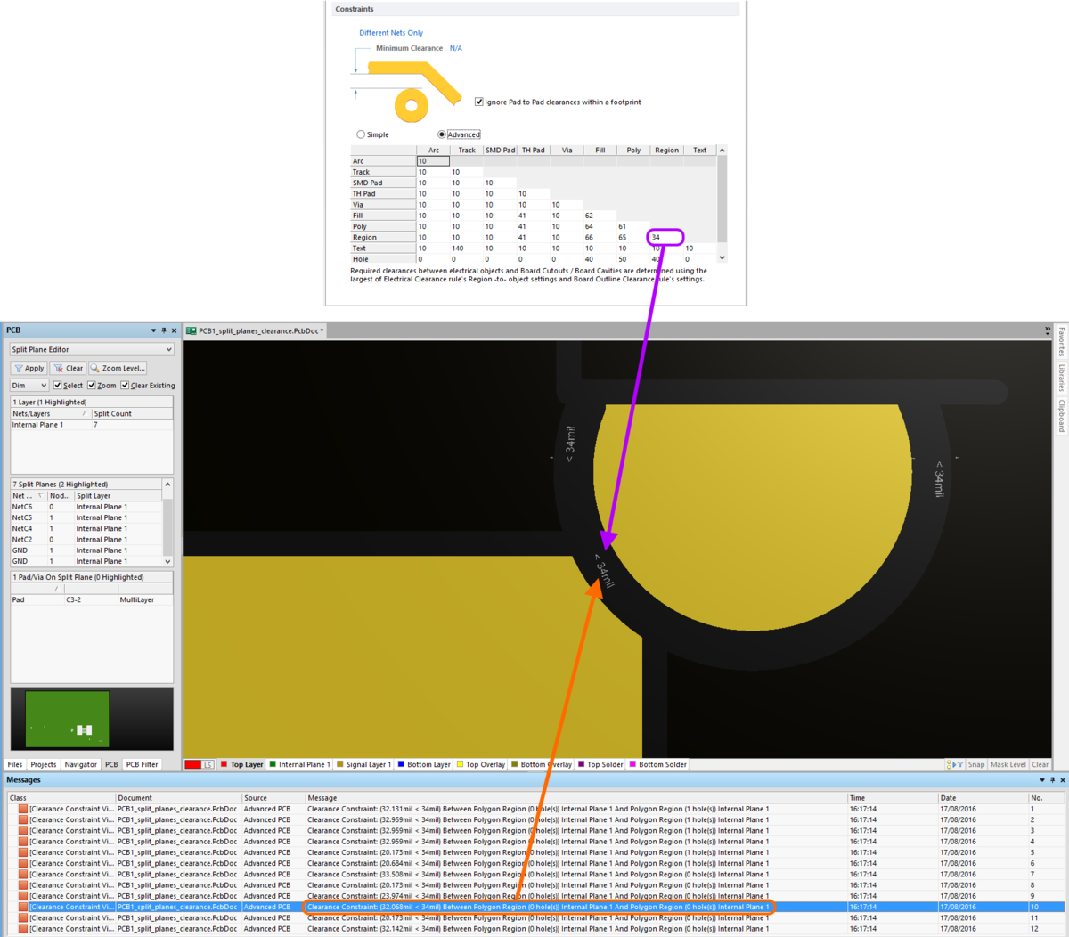
Split Plane Clearance Checking
Designers can also check clearances between split plane regions on internal plane layers. How clearance is defined depends on the mode in which you are using the minimum clearance matrix:
- Simple mode - specify the required split plane-to-split plane clearance value using the Copper-Copper cell.
- Advanced mode - specify the required split plane-to-split plane clearance value using the Region-Region cell.
A violation will appear in the form:
Clearance Constraint: (<CurrentClearance> < <DefinedClearance>) Between Split Plane (<NetName>) on <InternalPlaneLayerName> And Split Plane (<NetName>) on <InternalPlaneLayerName>,
for example:
Clearance Constraint: (32.36mil < 34mil) Between Split Plane (GND) on Internal Plane 1 And Split Plane (NetC6) on Internal Plane 1
![]() Clearance checking between split plane regions on an internal layer. In this case, the clearance value of 34mil has been entered in the Region-Region cell, as clearances
Clearance checking between split plane regions on an internal layer. In this case, the clearance value of 34mil has been entered in the Region-Region cell, as clearances
are being defined using the Advanced mode of the matrix.
Differential Pair Clearance Checking
Differential pairs present unique design challenges, often requiring a specific within-pair clearance as well as a pair-to-pair clearance, and potentially a third rule to control the pair-to-all other nets, clearance. To support this, the Constraints region includes the dropdown where you can choose Same Differential Pair and Different Differential Pair options.
For example, if the nets within the differential pairs require a tighter clearance than the general board clearance, this can be achieved by using the Same Differential Pair constraint option, as shown below. Note that even though the rule scope applies to All net objects in the design, the Constraint setting restricts it to only apply to objects in the Same Differential Pair.
![]()
This result could also be achieved by scoping the rule to only apply to differential pair objects (eg, InAnyDifferentialPair), as shown below. Note that this rule would also apply between a net in a differential pair to any other net object in the design, so this approach should only be used if you have other higher priority rule(s) that define the DiffPairNet-to-DiffPairNet and/or DiffPairNet-to-Any requirements. If this approach is used, the Priority of the differential pair rules must also be configured correctly, with the rule with a tighter clearance requirement having a higher priority.
![]()
A similar approach can be used to control the clearance between differential pairs. The image below shows how the Different Differential Pair constraint can be used to achieve this.
![]()
As with the previous example, it could also be achieved using the rule scope, instead of the Different Differential Pairs constraint. Remember that the rule priorities must be configured so the rule with the tighter clearance requirement has a higher priority.
![]()
To define a different clearance from a differential pair net to any other net object, the following rule could be used.
![]()
This could be further refined so that it only applies between differential pair objects and non-differential pair objects, as shown below.
![]()
► Learn more about scoping Differential Pair design rules
► Learn more about Differential Pair Routing
How Duplicate Rule Contentions are Resolved
All rules are resolved by the priority setting. The system goes through the rules from highest to lowest priority and picks the first one whose scope expressions match the objects being checked.
Rule Application
Online DRC, Batch DRC, interactive routing, autorouting, and during polygon placement.
Notes
- When defining the constraints for the rule, the Connective Checking option would typically be set to
Different Nets Only. An example of whenSame Net OnlyorAny Netcould be used is to test for vias being placed too close to pads or other vias on the same net, or any other net. - The minimum clearance matrix applies irrespective of the connective checking method specified. If different clearances are required between objects on the same net, to those defined for objects on different nets, be sure to define separate clearance rules as required to suit.
- The applicable use of the clearance matrix depends on the rule scoping. For example with scoping of ALL-ALL, all cells in the matrix are applicable (i.e. all possible object pairings). However, if scoping were set to IsVia-IsTrack, then only the single cell for the Via-Track object pairing would be applicable, and all other cells in the matrix left unused.
- When defining a clearance rule for a polygon, it is the primitives of the polygon that the rule is actually applied to, rather than the polygon itself. The keyword entry
InPolygon(orInPoly) should be included in the Full Query in this case, instead ofIsPolygon(orIsPoly). The specific polygon clearance rule must also be given a higher priority than any general clearance rule, if it is to have any effect. - When using the Dielectric Shapes Generator (in Printed Electronics), in Auto mode, the dielectric shape is automatically expanded to satisfy the requirement of the applicable Clearance Constraint design rule.
- In Printed Electronics, net to net clearances are tested on all layers, not just the same layer.