
教程 - 使用 Altium Designer 的完整设计流程演练
欢迎来到Altium电子产品开发世界。本教程将帮助您入门,通过整个过程指导您设计一个简单的PCB - 从想法到输出文件。
设计
您将要创建原理图并设计的印刷电路板(PCB)是一个简单的不稳定多谐振荡器。下面展示了电路图;它使用两个通用NPN晶体管配置成一个自运行的不稳定多谐振荡器。

多谐振荡器的电路

设计的PCB动画
登录Altium账户并连接到工作区
主要页面: 登录您的Altium账户, 访问您的工作区
Altium Designer 可以连接到一个工作区,以提供单一、安全的数据源和存储,同时提供无与伦比的协作能力。这可以是一个 Altium 365 工作区 —— 一个托管在 Altium 365 基于云的基础设施平台上的工作区,或者是一个 企业服务器工作区 —— 通过 Altium 本地企业服务器 提供的工作区,由您自己的 IT 部门安装和管理。
了解更多关于使用连接的工作区设计的信息
本教程重点介绍如何使用 Altium Designer 与连接的工作区 —— 满足您设计需求的流畅和强大的环境。要完成本教程,您需要连接到一个工作区。假设您的工作区已经激活/安装了示例数据。
首先,如果您还没有连接到您的Altium账户,您需要进行连接。您的Altium账户提供了对Altium即时服务的访问权限,包括连接到Altium 365工作区和制造商零件数据的权限。
-
当您未登录到您的Altium账户时,设计空间右上角的当前用户控件显示为
 。点击它,然后从关联菜单中选择
 项。
项。

-
在打开的登录对话框中,输入您的Altium账户凭据(邮箱和密码)并点击
 按钮。当前用户控件将变更为显示您已登录到您的Altium账户,通过显示您的Altium个人资料图片或头像(例如,
 )。
)。

-
确保您正在使用有效的Altium Designer许可证。许可证选择在通过点击当前用户控件并从关联菜单中选择
 项访问的许可证管理视图中执行。

参考许可证管理页面了解更多关于可用许可证类型及如何管理它们的信息。
-
通过在设计空间顶部的其标签上右键点击并从上下文菜单中选择关闭许可证管理命令来关闭许可证管理视图。

然后连接到您的工作区,无论是 Altium 365 工作区还是企业服务器工作区。当您未连接到工作区时,设计空间右上角的活动工作区控件显示为![]() 。
。
连接到 Altium 365 工作区
点击“活动工作区”控件,然后从关联菜单中选择您希望连接到的特定Altium 365工作区条目。活动工作区控件将变化,以反映您已连接到Altium 365工作区,通过显示工作区的名称(例如,![]() )。
)。

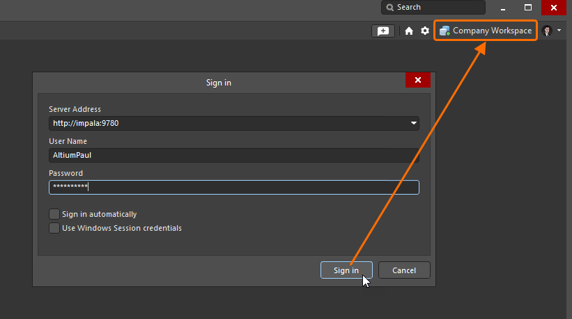
连接到企业服务器工作区
-
点击设计空间右上角的当前用户控件(例如,
),然后从关联菜单中选择 条目。
条目。

-
在打开的登录对话框中,输入工作区的URL(服务器地址)和您的工作区访问凭据(用户名和密码),然后点击
 按钮。活动工作区控件将变更,以反映您已通过显示工作区的名称连接到企业服务器工作区。
 AI 翻译
AI 翻译