
PCB
The PCB button is used to open the PCB panel. The button is accessed by choosing View | System | PCB from the PCB editor.

PCB Panel
The PCB panel allows you to browse the current PCB design using a range of filter modes to determine which object types or design elements are listed, highlighted, or selected. The panel also has editing modes for specific object types or design elements that provide dedicated controls for editing procedures. You also can access the properties for any element listed in the panel.


Setting the Visual Filtering
The visual result of the applied filtering on the document in the design editor window is determined by a series of highlighting controls toward the top of the panel. The effect that is imposed in the editor view can be set to Normal, Mask, or Dim; in practice, Mask has the most obvious highlighting effect.
The Normal/Mask/Dim drop-down list provides options for visibly contrasting filtered and unfiltered objects within the design editor window.

Confirm any changed settings by clicking the Apply button. Click the Clear button to return to the default settings.
Display Control
In Mask view mode, unfiltered (not selected) objects are monochrome. To set the contrast of the background (un-highlighted) objects, use the Mask Level slider control available in the Highlight & Edit Mask section from the PCB Editor's View tab.

Similarly, in Dim view mode, unfiltered objects retain their colors but are shaded. Set the balance between filtered and unfiltered objects using the Dim Level slider available in the Highlight & Edit Mask group under the View tab, as shown above.
Filter Options

Use the panel's checkboxes to apply the filter actions. Any combination of the options can be enabled. For example, you might want to have all filtered objects zoomed, centered, and selected in the design editor window. Click Clear to disable the currently-applied filter. All objects in the design space will become fully visible and available for selection/editing. If you want to reapply the filter, click Apply.
Panel Mini-viewer
The bottom section of the PCB panel provides a mini-viewer for the current document with an image of the current board design central to its window. A white viewing box is imposed on the image to show the area currently displayed in the design editor window. As the editor display automatically pans and zooms in response to the PCB panel filter selections, the box moves and expands accordingly to indicate the board viewing area.

As you manually pan around the document in the design editor window using the editor's horizontal and vertical scroll bars or the right-click panning hand, the viewing box in the panel will also move accordingly. Conversely, if you click inside the viewing box and drag it around the board image, the document in the design editor window will pan accordingly and at the current zoom level.
As you zoom in or out in the design editor window, the viewing box will be resized accordingly in the panel. Conversely, resizing the viewing box in the panel by clicking and dragging on any of its vertices will cause the zoom level to change in the design editor window. The smaller the size of the viewing box, the more the actual document has been zoomed-in.
Panel Modes
The PCB panel's functionality can change, depending on which mode is used. The different panel modes can be accessed and selected by clicking on the drop-down at the top of the panel.

A specific mode can also be accessed from the ribbon by choosing it from the View | PCB | PCB menu.

In any of the modes, as you click on an entry in a subsequent region of the panel a filter is applied essentially using the entry as its scope.
Nets
In Nets mode, the list regions of the panel will change to reflect an object hierarchy in order from the top:
- Net Class, as defined by the board.
- Individual member Nets within a class.
- Individual items (Primitives) within a Net (pads, vias, tracks, and fills).
Net Classes
In the top region of the panel (Net Class), right-click on a net or net item entry then choose Properties from the subsequent menu (or double-click on the entry directly) to access the Edit Net Class dialog in which you can view or edit the net membership of the class, rename it, or add additional classes.

Nets
The middle region of the panel displays nets from the Net Class(es) selected.

The following information is listed with each Net by default:
-
 - this feature has two functions:
- Color background - the color assigned to the net. This color is always applied to the net's connection lines. It can also be applied to that net's routing using the net color display override feature. Right-click then choose Change Net Color to edit the color for all currently selected nets.
- checkbox - check this to apply the color to the routing (enable the net color display the override feature) for this net. Right-click to enable (or disable) the display override feature for all currently selected nets. Press F5 to enable/disable net color display override in the workspace.
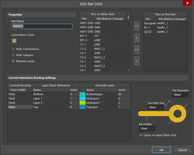
- Name - name of the net.
- Node Count - the total number of pads in this net.
- Routed Length - the sum of the lengths of the placed track and arc segments that form the routing, plus the vertical distance traversed through vias (see note below). The routed length calculator does not attempt to resolve overlapping track segments or routing wiggles inside pads.
- Un-Routed (Manhattan) Length - the vertical plus horizontal (X+Y) distance of all unrouted sections.
Right-click in the region then use the Columns sub-menu to add additional columns. In the image above, Min and Max have been added.
- Min/Max - settings from the applicable Length and Matched Length design rules. If there is no applicable rule(s) defined, the internal defaults of
Min=0milandMax=99999milare used.
Right-clicking on a Net then choosing Properties from the associated context menu (or double-clicking on the entry directly) will provide access to the Edit Net dialog in which you can view or modify the properties of the selected net or item.
Primitives
The display/inclusion of each net item type in the bottom Primitives region of the panel is dependent on whether the corresponding option for each has been enabled on the right-click menu, accessed from either the Nets or Primitives regions.
As you click on an entry in the panel's list, a filter will be applied based on that entry. The visual result of the selection (in the design editor window) is determined by the highlighting methods enabled (Dim, Zoom, etc.). Multiple entries can be selected in each region using standard Shift+Click and Ctrl+Click features.
Components
In Components mode, the three main regions will change to reflect an object hierarchy:
- Component Classes
- Components within a class
- Component Primitives
Right-click on a component or component primitive entry then choose Properties from the context menu or double-click on the entry directly to open the Inspector panel from where you can view/modify the properties of the component/primitive as required.
Right-click on a component class entry then choose Add Class or double-click on the entry directly to open the Edit Component Class dialog for that class. From the dialog, you can view/modify the component class membership, rename it, or add additional classes.

The display/inclusion of each component primitive type in the Component Primitives region is dependent on whether the corresponding option for each has been enabled on the right-click menu accessed from either the Components or Component Primitives regions.
As you click on an entry in the panel's list, a filter will be applied based on that entry. The visual result of the selection is determined by the highlighting methods enabled (Mask/Dim/Normal, Select, Zoom). Multiple entries can be selected in each region using standard Shift+click and Ctrl+click methods.
Split Plane Editor
This mode of the PCB panel allows you to easily view and manage split planes. A split plane is an enclosed region on an internal plane that divides the plane into separate electrically isolated areas.
The panel is split into the following regions:
- Layers - this region displays all internal plane layers currently defined in the design and how many split planes exist per layer.
- Split Planes - this region is filled with split planes contained in a selected entry from the Layers region.
- Pads/Vias On Split Plane - this region is populated with Pads and Vias from a selected entry in the Split Planes region of the panel.
Nets/Layers
The Nets/Layers region displays all internal plane layers currently defined for the design. Within the section, the Split Count column indicates how many split planes exist for the corresponding plane layer. A split count of '1' means that the layer has not been split and the layer itself is considered to be a single split.
Split Planes
After selecting an entry in the Layers region, all the split planes on that plane layer and their assigned nets will be loaded into the Split Planes region of the panel.
For each entry, a Node Count is displayed. This value reflects the total number of pads and vias that are connected to that split plane region.
Double-click (or right-click then select Properties from the context menu) on a Net with split planes to open the Split Plane dialog, which can be used to change to which net the split plane is assigned.

Filtering will be applied based on the entry chosen in the Layers region, the visual result of which is determined by the highlighting methods enabled (Mask/Dim/Normal, Select, and Zoom). Multiple entries can be selected using standard Shift+Click and Ctrl+Click features.
Pads/Vias On Split Planes
After selecting an entry in the Split Planes region of the panel, filtering will be applied based on that entry. Again, the filtering results depend on the highlighting methods enabled and whether pads and/or vias are enabled with respect to their visibility. Multiple entries can be selected in the region. Right-clicking on Pad or Via then selecting Properties from the context menu will open the associated Inspector panel for that primitive.
Differential Pairs Editor
This mode of the PCB panel can be used to create and edit differential pairs. Differential pairs can be added manually, through the Differential Pair Rule Wizard or created from nets.
The three regions of the Differential Pairs Editor mode of the PCB panel are:
- Differential pair classes.
- Individual member differential pairs within a class.
- The constituent nets (negative and positive) that form a differential pair.
As you click on an entry in a list, a filter will be applied based on that entry, the visual result of which is determined by the highlighting methods enabled (Mask/Dim/Normal, Select, Zoom). In this way, you can quickly highlight all differential pairs in a particular class, a particular differential pair, or a particular net that forms the negative or positive half of a differential pair. Multiple entries can be selected in each region using standard Shift+Click and Ctrl+Click features.
Right-clicking on a differential pair class entry then selecting Properties (or double-clicking on the entry directly) will open the Edit Differential Pair Class dialog in which you can rename or view/modify the differential pair membership of the class.
Right-click on a Differential Pair entry then select Properties or double-click on the entry directly to open the Differential Pair dialog in which you can view/modify the properties for differential pair name and its constituent nets.
Right-click on a Net(s) entry in the PCB panel then selecting Properties (or double-clicking on the entry directly) will open the Edit Net dialog in which you can view/modify the properties of the net as required.
In the PCB panel, as you click on an entry in a list, a filter will be applied based on that entry. The visual result (in the design editor window) of the cumulative filter is determined by the highlighting methods enabled (Mask/Dim/Normal, Select, Zoom). Using these highlighting methods, you can quickly highlight all differential pairs in a particular class, a particular differential pair, or a particular net that forms the negative or positive half of a differential pair. Multiple entries can be selected in each region using standard Shift+Click and Ctrl+Click features.
Managing Differential Pairs
Use the Differential Pairs region of the panel to manage the differential pair objects in a design. For the particular differential pair class selected, all currently defined differential pair objects that belong to that class will be listed in this region.
Use the Add, Delete and Edit buttons at the bottom of this region to create new differential pair objects, or edit or delete existing ones. These three commands are also available from the right-click menu for the region. When adding a new differential pair, the Differential Pair dialog will open.
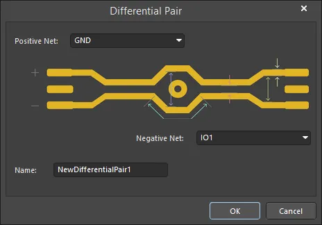
Use the dialog to define the pair object, in terms of a positive and negative net and a meaningful name. By default, the name will be set to NewDifferentialPair1 and the positive and negative nets will be set to the first and second available nets in the netlist for the design. Use the drop-down lists to select from the available nets.
Note that only available nets are listed for selection. Nets currently defined as part of existing differential pairs are not listed.
When editing an existing differential pair object, the Differential Pair dialog will open with the currently chosen nets for the pair entered into the Positive Net and Negative Net drop-down fields. Change one or both nets for the pair or rename the pair as required.
Creating Differential Pairs from Design Nets
Differential pair objects can be automatically created from the nets in your design using the Create Differential Pairs From Nets dialog. This dialog is accessed by clicking on the Create From Nets button at the bottom of the Nets region of the PCB panel.
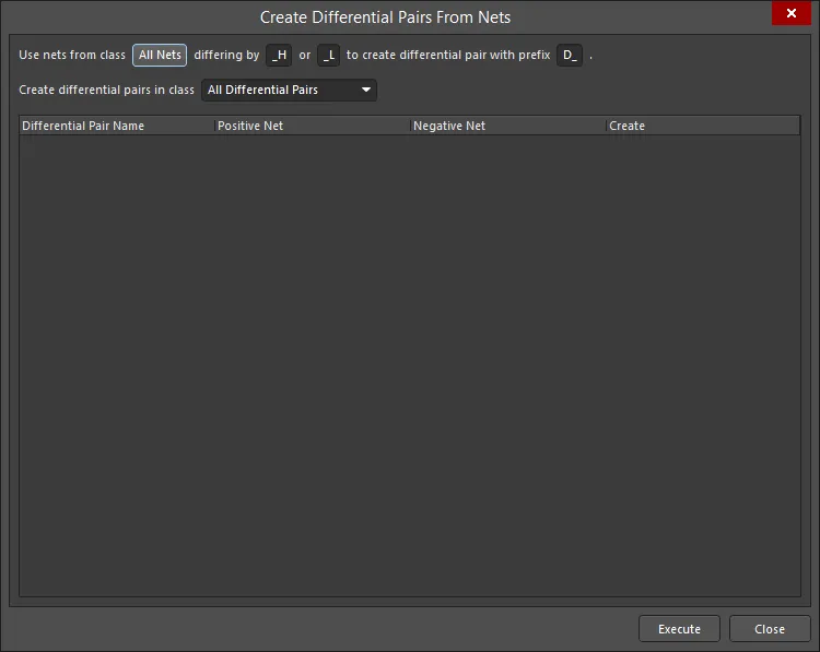
The effectiveness of this automated method directly depends on the naming convention that has been used for the specific nets that will make up the differential pairs. Ideally, a naming convention will be used so that a common root is followed by a consistent positive/negative indicator (P and N). For example, consider the receiver signal D_ETH_O.RX, which is a differential signal in the design. The two nets that constitute this signal are ETH_O.RX_P and ETH_O.RX_N - these represent the positive and negative sides of the signal, respectively.
The filters at the top of the dialog enable you to quickly target these nets in terms of the net class to which they belong and the particular differentiating factor that has been used to distinguish the positive and negative nets in an intended pairing, for example, _P and _N. You can also define a prefix to be added to the differential pair objects created, and also determine in which differential pair class they are to be added.
For each differential pair object, the dialog lists its constituent positive and negative nets. By default, all prospective differential pair objects are selected for the creation and individual ones can be excluded by clearing the associated Create checkbox.
When all options are set as required, click the Execute button - the differential pair objects will be created and the PCB panel will update accordingly.
Filtering will be applied to show the created pairs in the design space.
Configuring Applicable Design Rules
A Differential Pair Routing rule needs to be configured before routing a differential pair in a design. A differential routing rule defines:
- The preferred Gap between the network pair, and its permitted range.
- The maximum Uncoupled Length (the pair is uncoupled when the gap is wider than the maximum Gap setting).
- The preferred routing Width for each net.
- The optional gap/width setting variations for each layer in the stack.
- The scope (in terms of classes and objects) for the rule's application.
While rules can be created manually using the PCB Rules and Constraints Editor dialog, the PCB panel offers the convenience of the Differential Pair Rule Wizard dialog. Use the Rule Wizard button (below the Nets region in the PCB panel) to access the Wizard and implement the rule properties as required.

Note that the scope of the rules will depend on the selection in the PCB panel prior to launching the wizard, as follows:
Differential Pair Class
If the All Differential Pairs class is selected, the scope will be All for each rule.
If a specific differential pair class is selected, the scope will be InDifferentialPairClass('ClassName') for each rule.
Differential Pair
If a single differential pair object is selected in the panel, the scope will be:
- Width -
InDifferentialPair('PairName')
If multiple differential pair objects are selected in the panel, there will be individual scope entries for each pair object, each separated by an 'Or' operator. For example, a routing Width rule targeting individually selected differential pair objects D_ETH_O.TX and D_ETH_O.RX will have a scope of:
InDifferentialPair('D_ETH_O.TX') Or InDifferentialPair('D_ETH_O.RX')
Note that the clearance from a net in a differential pair to any other electrical object that is not a part of the pair is monitored by the applicable Clearance rule.
To edit the configuration of an existing Differential Pairs Routing rule, including its scope, open the PCB Rules and Constraints Editor dialog (Home | Design Rules) then navigate to Routing - Differential Pairs Routing.
Polygons
The three main regions of the panel are, in order from the top:
- Polygon Classes.
- Individual Polygons within a class.
- Individual primitives that constitute a Polygon.
Right-click on a polygon entry then selecting Add Class to open the Edit Class dialog in which you can edit and add Polygon Classes.
Right-click on a polygon entry or a polygon primitive entry then select Properties (or double-click on the entry) to open the Inspector panel in which you can view/modify the properties as required.
In the panel's Polygon Primitives region, the display/inclusion of each polygon primitive type is dependent on the setting of the corresponding enabling option accessed from the right-click menu as shown below.
As you click on an entry in the panel's list, a filter will be applied based on that entry where the visual result of which is determined by the enabled highlighting methods (Dim, Zoom, etc.). Multiple entries can be selected in each region using standard Shift+Click and Ctrl+Click features.
Hole Size Editor
In the PCB panel’s Hole Size Editor mode, the three main regions of the panel will change to reflect:
- The general filtering for hole types and their status, with a sub-section for the layer drill pairs currently defined for the board.
- Hole objects arranged in groups as determined by size and shape.
- Individual primitives that constitute each group of hole objects (pads, vias, and slots).
The groups of holes can be collectively edited in the Unique Holes region of the panel by entering values in the appropriate column cell. You can enter a numeric value to change the current hole size for pads and vias in the Hole Size column. You can also change the corresponding Hole Length, Hole Type, and Plated entries for holes where applicable using the drop-downs.

Individual pad/via objects belonging to the selected holes group are listed in the Pad/Via region. Right-click on an object in the list then select Properties (or double-click on the entry directly) to open the associated mode of the Inspector panel or that primitive where its properties can be viewed and edited.
As you click on an entry in the panel's lists, a cumulative filter will be applied based on that entry. The visual result of this (in the design editor window) is determined by the highlighting methods enabled (Mask/Dim/Normal, Select, and Zoom). Using the highlight methods, you can quickly highlight all holes of a particular status, style or size, or an individual hole primitive (pad/via) that exists in that filtered group. Multiple entries can be selected in each list section using standard Shift+Click and Ctrl+Click features.
3D Models
The three main regions of the panel when in 3D Models mode are:
- Component Classes
- Specific Components associated with the component class that have associated 3D body object(s) or free models (non-PCB mounted, free-floating 3D bodies)
- The individual 3D bodies for each component or free Model(s)
As you click on a specific component in the Components region of the panel, filtering will be applied using the component as the scope of the filter. The visual result is determined by the highlighting methods enabled (Mask/Dim/Normal, Select, and Zoom). Multiple rule entries can be selected using standard Shift+Click and Ctrl+Click features.
Double-clicking a component entry in the Components or Models region of the panel (or right-click then choose Properties) to open the associated mode of the Inspector panel where you can edit its properties in detail.
When selecting a component's constituent models from the Models list, the view in the editor will zoom, dim/mask, or select accordingly.
The PCB panel can be used to select display properties for 3D models. The cone icons ( ) represent different levels of transparency from 100% (hidden) to 0% (solid) in increments of 25%. You can select multiple components and apply the same display controls to them at once using the Highlighted Models options.

Toggle in the DRC column to enable or disable Design Rule Checking of 3D object types that contain a STEP model. Click once to uncheck (disable) the feature or click twice to check (enable) the feature.

Multiple model entries can be selected using standard Shift+Click and Ctrl+Click features providing full control over the 3D Model view and the base 3D elements that make up a component.
Right-click Menu
The following key options are on the right-click menu of the PCB panel. The actual content of the menu varies depending on the current mode of the panel and the particular region of the panel from where the menu is accessed:
- Report - generate a report in context with the section of the panel the menu is accessed from. After launching the command, the Report Preview dialog will open from where you can peruse, print, and export the report in various file formats.
- Properties - access the corresponding panel for the chosen object, from where you can view/modify the properties for that object. For example, with a component entry selected, using this command will access the Component mode of the Inspector panel.
Notes
- Ctrl+Click over a selected entry to deselect it. If the entry is the only one selected for that region, performing this action will clear the filter.
- In sections of the panel where multiple columns of data exist, the data can be sorted by any column by clicking on the header for that column. Clicking once will sort in ascending order; click again to sort by descending order.
- You can change the order in which columns of data are displayed. To move a column, click on its header then drag it horizontally to the required position. A valid position is indicated by the appearance of two green positional arrows.