The area that the component occupies on the fabricated board is defined by the component footprint. A typical footprint includes pads and a component overlay, and can also include any other mechanical details required. In the example footprint below, most of the component outline is defined on a mechanical layer (the green lines) rather than the (yellow) overlay, because this component will be mounted so that it hangs over a cutout in the board.

The footprint defines the space the component occupies and provides the points of connection from the component pins/pads to the routing on the board.
The component that is mounted on that footprint can be modeled using 3D Body objects. The 3D Body object is used as a container into which a generic MCAD format model can be imported, as shown in the image below.

A suitable MCAD model can be imported into a 3D Body object.
Even with a rich set of resources providing ready-made PCB components (such as the Manufacturer Part Search panel), it is likely that at some point in your career, you will need to create a custom PCB component. PCB component footprints are created in the PCB Footprint editor using the same set of primitive objects available in the PCB editor. In addition to footprints, company logos, fabrication definitions, and other objects required during board design can also be saved as PCB components.
Creating a New PCB Footprint
Footprints can be created directly in your connected Workspace. To do this:
-
Select File » New » Library from the main menus, then in the New Library dialog that opens, select Create Library Content » Footprint from the Workspace region of the dialog.

Create a new Workspace Footprint using the New Library dialog
-
In the Create New Item dialog that opens, enter the required information, make sure that the Open for editing after creation option is enabled and click OK. The Workspace Footprint will be created and the temporary PCB Footprint editor will open, presenting a .PcbLib document as the active document. This document will be named according to the Item-Revision, in the format: <Item><Revision>.PcbLib (e.g., PCC-001-0001-1.PcbLib). Use the document to define the footprint as described below.

Example of editing the initial revision of a Workspace Footprint – the temporary PCB footprint editor provides the document with which to define your footprint.
-
When the footprint is defined as required, save it to the Workspace using the Save to Server control to the right of the footprint's entry within the Projects panel. The Edit Revision dialog will appear, in which you can change Name, Description, and add release notes as required. The document and editor will close after saving.
A saved Workspace Footprint can be used when defining a component using the Component Editor in its Single Component Editing mode or Batch Component Editing mode.
Workspace Footprints can be browsed using the Components panel. Enable visibility of models by clicking the  button at the top of the panel and selecting Models, then select the Footprints category.

To edit a Workspace Footprint, right-click its entry in the Components panel and select the Edit command. Once again, the temporary editor will open, with the footprint opened for editing. Make changes as required, then save the document into the next revision of the Workspace Footprint.
When saving an edited footprint to your Workspace, you can preserve the footprint's current lifecycle state. Control is provided courtesy of the Preserve lifecycle state (not recommended) option available in the Create Revision dialog when re-saving ( ). When the option is enabled, the new footprint revision will automatically be set to the lifecycle state of the previous revision. This ability is available for those with assigned Allow to skip lifecycle state change for new revisions operational permission (learn more about Setting Global Operation Permissions for a Workspace).
Updating Related Component
When you make a change to a Workspace domain model – be it a symbol, footprint model, or simulation model – the moment you save that change into a new revision of the model, any Workspace Components that use that model will become effectively out of date, still using the previous revision. In most cases, you will no doubt want to re-save those Workspace Components, with the respective model links updated to use the latest revisions available. To streamline this process, a Workspace, in conjunction with Altium Designer, facilitates the ability to update related components – at the point of re-saving a Workspace model – after having made any modifications to that model through the direct editing feature.
The option to perform this update to the parent components can be found in the Create Revision dialog that appears when saving the modified Workspace Footprint back to the target Workspace. This option – Update items related to <ModelItemRevision> – is enabled by default.
<ModelItemRevision> is the current revision of the model, that is, the revision currently being used by any related Workspace Components. Once the Workspace model itself is saved, this would naturally be the previous (earlier) revision, and no longer the latest.

Accessing the option to update related Workspace Components, that are referencing the Workspace Footprint being re-saved.
If you want to keep all related components using the current revision of the Workspace Footprint, disable this option. Only the Workspace model itself will then be saved.
Once you click OK in the Create Revision dialog, the modified footprint is saved back to the Workspace, and its associated temporary editor is closed. All Workspace Components referencing that Workspace Footprint will be re-saved to use its new revision automatically (the next revision of each component is automatically created and the save performed).
-
From a designer's perspective, a Workspace Component gathers together all information needed to represent that component across all design domains, within a single entity. It could therefore be thought of as a container in this respect – a 'bucket' into which all domain models and parametric information is stored. In terms of its representation in the various domains, a Workspace Component doesn't contain the Workspace domain models themselves, but rather links to these models. These links are specified when defining the component.
-
PCB footprints can also be created in the Workspace as part of importing existing, older generation (SchLib, PcbLib, IntLib, DbLib, SVNDbLib) libraries of components. The interface to this process – the Library Importer – presents an intuitive flow that takes initial selected libraries, and imports them to your Workspace. Learn more about the Library Importer.
-
A new Workspace Footprint can also be created when defining a Workspace Component in the Component Editor in its Single Component Editing mode.
-
A footprint can also be created as part of a file-based PCB footprint library.
Defining a PCB Footprint
Footprints are always built on the top side, regardless of which final side of the board they are placed, using the same set of tools and design objects available in the PCB editor. Layer-specific attributes, such as surface mount pads and solder mask definitions, are automatically transferred to appropriate bottom-side layers when you flip the footprint to the other side of the board during component placement.
Design objects can be placed on any layer, however, the outline is normally created on the Top Overlay (silkscreen) layer and the pads on the multi-layer (for thru-hole component pins) or the top signal layer (for surface mount component pins). When you place the footprint on a PCB, all objects that make up the footprint will be assigned to their defined layers.

2D and 3D views of a footprint for a joystick component. The 3D image shows the imported STEP model for the component. Note that the pads and component overlay can be seen below the STEP model.
The footprints shown on this page are only to illustrate the procedures required; they are not dimensionally accurate. Always check the specifications of a new footprint against the manufacturer's datasheet.
The typical sequence for manually creating a component footprint is:
-
Prepare the design space: define snap options, configure grids and guides - learn more.
-
Footprints should be built around the design space reference point at the center of the PCB footprint editor. This reference point is actually the relative origin for the design space and is the point by which the component footprint is picked-up by the cursor in Place and Move operations (depending on the current Object Snap Options in the PCB Editor – General page of the Preferences dialog). Use the J, R shortcut keys to jump directly to the reference point. If you have forgotten to move to the reference point before beginning to build your footprint, you can bring the reference pad to your footprint using the Edit » Set Reference sub-menu commands:
-
Pin 1 - set the component reference point to be pin 1 of the component footprint.
-
Center - set the component reference point to be the center of the component footprint.
-
Location - set the component reference point to a user-defined location.
The chosen point will be set to 0,0 - it becomes the new relative origin and all primitives will have their locations updated relative to this point.
-
Place the pads (Place » Pad) according to the component requirements. After running the Place Pad command but prior to placing the first pad, press the Tab key to open the Properties panel to define all the pad properties, including the pad Designator, Size and Shape, Layer, and Hole Size (for a thru-hole pad). The Designator automatically increments for subsequent pad placements. For a surface mount pad, set the Layer to Top Layer. For a thru-hole pad, set the Layer to Multi-Layer.
Some footprints require pads that have an irregular shape. This can be done using pad objects of Custom Shape. To learn more, refer to the
Customizing a Pad Stack page.
-
One of the most important procedures in creating a new component footprint is placing the pads that will be used to solder the component to the PCB. These must be placed in exactly the right positions to correspond to the pins on the physical device.
-
Some care should also be exercised when designating pads since it is this property that Altium Designer uses when mapping from pin numbers on the schematic symbol.
-
To ensure accurate placement of the pads, consider setting up a grid specifically for the task. Use the Ctrl+G shortcut keys to open the Cartesian Grid Editor dialog and the Q key to toggle the grid from Imperial to Metric.
-
To accurately place a pad while moving it with the mouse, use the keyboard arrow keys to move the cursor in current grid increments. Additionally, holding Shift will move in steps of 10 times the grid. The current X, Y location is displayed on the Status bar and also in the Heads Up display. The Heads Up Display contains both the location and the delta from the last click location to the current cursor location. Use the Shift+H shortcut to toggle the Heads Up display on and off. Alternatively, double-click to edit a placed pad and enter the required X and Y locations in the Properties panel.
-
To check a distance between two points in the design space, use the Reports » Measure Distance (shortcut Ctrl+M). Follow the prompts on the Status bar.
-
Pad-specific attributes, such as solder mask and paste mask, are automatically calculated based on the pad dimensions and applicable mask design rules. While mask settings can be defined manually for each pad, doing so makes it difficult to modify these settings later during the board design process. Typically this is done only when it is not possible to target the pads by design rules. Note that rules are defined in the PCB editor during board design.
-
Use tracks, arcs and other primitive objects to define the component outline that appears on the PCB silkscreen on the Top Overlay layer. If the component is flipped to the bottom of the board during placement, the overlay is automatically transferred to the Bottom Overlay layer.
-
Place tracks and other primitive objects on a mechanical layer to define extra mechanical detail, such as a placement courtyard. Mechanical layers are general-purpose layers. You should allocate the function of these layers and use them consistently across their footprints.
-
Place 3D Body objects to define the three-dimensional shape of the physical component to be mounted on the PCB.
-
The Designator and Comment strings are automatically added to the footprint’s Overlay layer during placement into the PCB design space. Additional Designator and Comment strings can be included by placing the .Designator and .Comment special strings on a mechanical layer.
When placing Designator and Comment strings, a Layer Pair needs to be defined in the PCB editor. This ensures that the strings will be tied to the side of the board on which the component is mounted and must flip to the other side of the board when the component is flipped. For more information, see the
Handling Special Layer-specific Requirements section below.
-
Define the properties of the footprint (e.g., its name and description) on the Footprint tab of the Properties panel in its Library Options mode (active when no object is selected in the design space, can be accessed using the Tools » Footprint Properties command from the main menus). Refer to the section below to learn more about the options and controls available under the panel's Footprint tab.
-
For a standardized pad/via definition across all footprints, the Pad/Via library (*.PvLib) can be used for Pad/Via placement – learn more.
-
The PCB Footprint editor also provides some Wizards to expedite the footprint creation process:
-
The IPC Compliant Footprint Wizard – generates a PCB footprint that is truly compliant with Revision B of the IPC standard 7351 – Generic Requirements for Surface Mount Design and Land Pattern Standard – learn more.
-
The IPC Compliant Footprints Batch Generator – when working with a file-based PCB footprint library, use the IPC Compliant Footprints Batch Generator to quickly generate multiple footprints, at multiple density levels – learn more.
-
The Footprint Wizard – allows you to select from various package types and fill in appropriate information and it will then build the component footprint for you – learn more.
Preparing the Design Space
The default is to display the grids using dots. If you prefer, grids can be displayed using lines. This is configured in the Grid Editor dialog, accessed by clicking the Properties button in the Properties panel as shown in the image below. Alternatively, press the Ctrl+G shortcut to open the dialog.

In the image, the fine grid is displayed as dots, and the coarse grid is displayed as lines.
Properties Panel
When editing a footprint in the PCB footprint editor and when no design object is currently selected in the design space, the Properties panel presents the Library Options.
The following collapsible sections contain information about the options and controls available under the panel's General tab:
Selection Filter
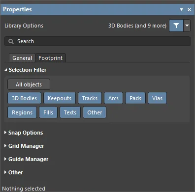
The options in this section of the panel determine which PCB footprint objects may be selected in the design space.
-
All Objects button – select remove object filtering so that all types of objects may be selected.
-
Object buttons – toggle each object button to enable/disable the ability to select that object type.
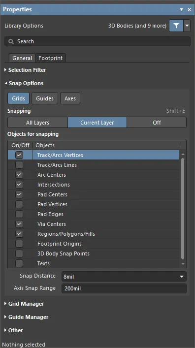
Snap Options
-
Grids – used to toggle whether the cursor will snap to the active design space grid. When this option is enabled the cursor will pull, or snap, to the nearest snap grid location. The active snap grid is displayed on the Status bar, and in the PCB editor Heads Up display (Shift+H shortcut to toggle on/off).
-
Guides – used to toggle whether the cursor will snap to manually placed linear or point Snap Guides. A Snap Guide will override the Snap Grid.
-
Axes – used to toggle whether the cursor will axially align (in either the X or Y direction) to the enabled Objects for snapping. The Axis Snap Range defines the distance within which X or Y axial alignment will occur. A dynamic alignment guideline is displayed when alignment is achieved from the current cursor location to the axially-aligned object snap point (hotspot).
-
Snapping – select directly or use the Shift+E shortcut to select whether you want to snap to objects on:
-
All Layers – enable this option to allow the cursor to snap to any electrical object on any visible layer.
-
Current Layer – enable this option to allow the cursor to only recognize and snap to objects placed on the currently selected layer.
-
Off – enable this option to turn off snapping to hotspots.
-
Objects for snapping
-
On/Off – check to enable snapping for the desired objects.
-
Objects – a list of the available objects.
-
Snap Distance – when the cursor is within this distance from an enabled object snap point (and snapping is enabled for the active layer), the cursor will snap to that point.
-
Axis Snap Range – when the cursor is axially aligned and within this distance from an enabled object snap point (and the Axes button is enabled), a dynamic guideline will display to indicate that alignment has been achieved.
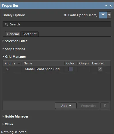
Grid Manager
-
Grid Manager – where local customized grids can be defined and managed, as well as the default Snap Grid for the board.
-
Priority – in the design space, priority is distinguished by drawing order. The highest priority grid (priority
1) will be drawn in front of all other grids, then the grid with priority level 2, etc., down to the default Global Board Snap Grid, which is drawn behind all other custom grids.
-
Name – displays the name of the grid.
-
Color – click to open a drop-down to set/change the color of the associated grid.
-
Enabled – check to enable the associated grid.
-
Add
-
Add Cartesian Grid – click to add a Cartesian grid.
-
Add Polar Grid – click to add a Polar grid. Polar grids enable you to more easily design non-rectangular features and boards.
-
Properties – click to open the respective grid editor dialog (Cartesian Grid Editor or Polar Grid Editor) to modify properties for the selected grid.
-
 – click to delete the currently selected grid.
Guide Manager
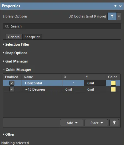
-
Guide Manager – where a range of manual Snap Guides and Snap Points for the board can be defined and managed.
-
Add – click to add a new snap guide or snap point. Choose the corresponding command for the required guide type from the associated menu; an entry for the new guide/point will be added to the grid. The following guide types are available:
-
Add Horizontal Guide – use this command to add a horizontal guideline at the desired Y-coordinate location in the design space.
-
Add Vertical Guide – use this command to add a vertical guideline at the desired X-coordinate location in the design space.
-
Add +45 Guide – use this command to add a 45 degree (y=x) guideline that passes through the desired X,Y coordinate location in the design space.
-
Add -45 Guide – use this command to add a -45 degree (y=-x) guideline that passes through the desired X,Y coordinate location in the design space.
-
Add Snap Point – use this command to add a point snap guide. This is a hotspot that you manually mark within the confines of the default snap grid. During an interactive process such as placing or moving an object, that objects' hotspot will 'snap' to a point snap guide when it passes into close proximity with it.
-
Place – click to place a guide. Select the guide type from the drop-down:
-
Place Horizontal Guide – use this command to place a horizontal guideline at the desired Y-coordinate location in the design space.
-
Place Vertical Guide – use this command to place a vertical guideline at the desired X-coordinate location in the design space.
-
Place +45 Guide – use this command to place a 45 degree (y=x) guideline that passes through the desired X,Y coordinate location in the design space.
-
Place -45 Guide – use this command to place a -45 degree (y=-x) guideline that passes through the desired X,Y coordinate location in the design space.
-
Place Snap Point – use this command to place a point snap guide. This is a hotspot that you manually mark within the confines of the default snap grid. During an interactive process such as placing or moving an object, that objects' hotspot will 'snap' to a point snap guide when it passes into close proximity with it.
-
– click to delete the currently selected guide.
Other
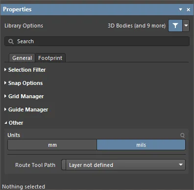
-
Units – use to select the default measurement units for the current PCB footprint document. Default units are used to display any distance-related information on screen or in reports. The default units are always used if a unit's suffix (mm or mil) is not entered when specifying any distance-related information.
-
Route Tool Path – use the drop-down to choose the mechanical layer (from all those currently enabled for use in the design) on which to define the route tool path for the board.
The following collapsible sections contain information about the options and controls available under the panel's Footprint tab:
The ability to define footprint properties using the Footprint tab of the Properties panel is available when the PCB.FootprintParameters option is enabled in the Advanced Settings dialog. When this option is disabled, footprint properties are defined using the PCB Library Footprint dialog ( ) accessed by selecting the Tools » Footprint Properties command from the main menus, or by selecting a footprint entry in the Footprints region of the PCB Library panel and clicking the Edit button, or by double-clicking a footprint entry in the Footprints region of the PCB Library panel.
When a design object is selected, the panel will present options specific to that object type. The following table lists the object types available for placement within the PCB footprint design space – click a link to access the properties page for that object.
Solder and Paste Mask Expansions
To check that solder and/or paste masks have been correctly defined in the PCB footprint editor, open the View Configuration panel and enable the show option ( ) option for each mask layer.
The ring that appears around the edge of each pad in the color of the Top Solder Mask layer represents the edge of the solder mask shape protruding by the expansion amount from under the multi-layer pad because multi-layer is at the top of the layer drawing order; it is drawn on top. The Layer Drawing Order is set on the PCB Editor - Display page of the Preferences dialog).
The image below shows a PCB footprint with a purple (color of the Top Solder Mask layer) border that appears around the edge of each pad.

To quickly walk through layers, use the Single Layer Mode (Shift+S) in combination with Ctrl+Shift+Wheel roll.
By default, the shape that is created on the mask layers is the pad shape, expanded or contracted by the amount specified by the Solder Mask Expansion and Paste Mask Expansion design rules set in the PCB on which the footprint is placed. In some cases, you might need to override the expansion design rules and specify a mask expansion as a pad attribute, select from a standard set of predefined mask shapes, or create your own custom shape. In these situations, you can configure paste/solder masks for a selected pad in its Properties panel - learn more. Alternatively, you can place suitable primitives (Regions, Tracks, etc.) on the required mask layer.
In a PCB library, all objects with rule-driven solder mask expansion will have the expansion value equal to 0 mil. This feature is available when the PCB.SolderMaskZeroExpansion option is enabled in the Advanced Settings dialog. When this option is disabled, the solder mask expansion value for such objects in a PCB library is 4 mils.
Parameter Support
Parameters applied to objects in Altium Designer provide a powerful and flexible means of adding additional information to a PCB design. Applied as properties of the parent object, parameters can be applied at a range of levels, including projects, documents, templates, and individual objects within a design document.
Parameters that become available in the PCB space can be used to filter Queries, Design Rules, Scripts, and Variants, and can be applied in PCB component footprints for invoking custom strings in placed Footprints.
Parameters via an Engineering Change Order
The PCB parameter capabilities are based on functionality included in the ECO mechanism and PCB document, which allow user-defined component parameters to be transferred to and retained in the PCB space. This is a one-way transfer and the passed parameters are read-only in the PCB domain.
The parameter transfer is done by creating an ECO from the schematic to PCB with the Design » Update PCB Document menu command.

When the ECO is executed (by using the Execute Changes button), any new user-defined schematic component parameters will be transferred to the corresponding footprint reference in the PCB design.
The detection and migration of parameters to the PCB is determined by the project's options settings (Project » Project Options). In the Project Options dialog, set the difference detection and modification behavior in the Differences Associated with Parameters section of the Comparator tab and the Modifications Associated with Parameters section of the ECO Generation tab.
To view the transferred parameters in the PCB editor, double-click a component to open the Properties panel then choose the Parameters tab. The tab will list the current user parameters that have been assigned to the selected component footprint. Parameters for a selected component footprint also are available in the Components panel.
Information Reference Links
The PCB domain automatically accepts the predefined ComponentLink parameters from the schematic. These are defined as parameter pairs (Description and link URL) that normally establish data reference links to specific files or internet locations – typically a manufacturer web site or datasheet URL.
In both the schematic and PCB design space, the links are accessed from the right-click context menu when hovering over a component (under the References sub-menu options). The specialized parameters are added in the Properties panel, and when transferred to the PCB space, they appear as a component footprint parameter.

Parameters in Source Footprints
Parameters passed to the PCB can be used for providing additional board production or functional information via component footprints. By adding special parameter strings to footprints at the source library level, the custom strings will be interpreted on the target mechanical layer or overlay.
A special string representing a user-defined parameter can be added to the source component footprint using the special strings button and drop-down ( ) in the Properties panel.

In the below library footprint, the special string .Designator has been placed on the Mechanical 2 layer.

A special string representing a user parameter can be added to the component footprint.
When that custom parameter has also been applied to schematic components and the parameter data has been transferred to the PCB, the interpreted footprint strings will appear on both the board view and generated output files. In this case the special parameter string contains a custom component part identifier to aid assembly.
The application of the user parameters to component footprints as special strings can serve a range of other custom PCB requirements, including function labels for switches and connectors, where a 'function' parameter string might be placed on the Top Overlay in footprints for those component types.
To see the interpreted value of special strings on the board layout, enable Special Strings option under the Additional Options region of the View Options tab in the View Configuration panel. Special strings are always converted in generated output files.
In the schematic editor, if desired, enable the Display Names of Special Strings that have No Value Defined option on the Schematic – Graphical Editing page of the Preferences dialog.
Parameter Queries
Parameter strings in the PCB domain are also accessible through the Altium Designer query language, and therefore, are available for object filtering functions, including the Find Similar Objects feature.
To perform a similar objects selection, right-click on a component then select Find Similar Objects from the context menu to open the Find Similar Objects dialog.

The Find Similar Objects dialog includes a Parameters section where the filtering options can be selected as required.

The PCB Filter panel can apply parameter-specific query words as filter criteria, and can be used for creating Design Rules based on PCB parameters.
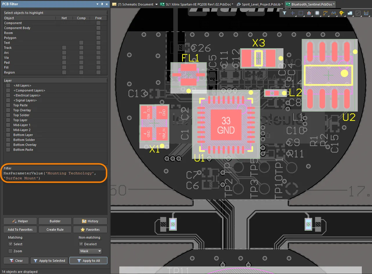
Several query words are available for working with PCB footprint parameters, including specific function words for converting string values to numbers (such as StrToNumber). The string Value conversions are unit-aware (V, mA, mV, kOhm, etc.) and allow the query result to be determined by the numerical processing of a parameter value string.
The supported Unit Types that can be nominated in the queries are:
-
% – Percent
-
A – Current
-
C – Temperature
-
dB – Decibels
-
F – Capacitance
-
G – Conductance
-
H – Inductance
-
Hz – Frequency
-
Kg – Mass
-
m – Length
-
Ohm – Resistance
-
Q – Charge
-
s – Time
-
V – Voltage
-
W – Power
-
Z – Impedance

Several Parameter query words are available for working with PCB component footprint parameters.
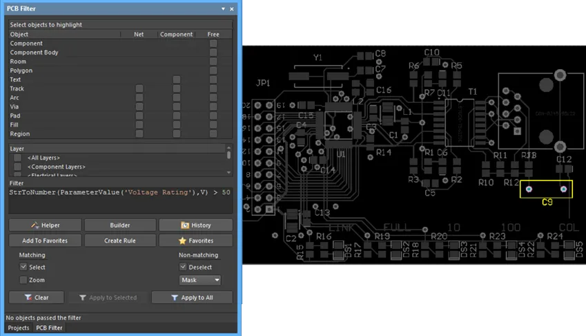
The example shown in the Query Helper dialog above processes the Voltage Rating parameter for each component (using the string-to-number conversion – StrToNumber(Unit Value, Unit Type)) to determine if its value is greater than 50V. When applied in the PCB Filter panel, the example board layout exposes a single high-voltage component, C1 (which has a Voltage Rating value of 3kV).
Scientific E notation is also supported, so, for example, a query to filter capacitor values over 1nF would be similar to:
StrToNumber(ParameterValue('CapacitanceValue'), F) > 1e-9
Alternatively, the number conversion function could be used for both the returned ParameterValue and the comparison value:
StrToNumber(ParameterValue('CapacitanceValue'), F) > StrToNumber('1nF', F)
Rules and Scripts
PCB parameter queries can also be applied to Altium Designer Scripts and Design Rules. The latter might perform layout validation checks, such as detecting footprint parameters in order to assess component placement or layer assignment. Note that the functions listed in the Query Helper dialog above are available to the Scripting language.
The below example shows the capacitor voltage rating query (see the filter query above) applied to a component placement rule, which, when run, checks for specific clearance values for components detected as high voltage (>50V) devices.

Design rules defined by specific footprint parameters, as transferred from the schematic space, can be used for detecting custom layout conditions.
Similarly, custom PCB parameters can be used to check component layer compatibility, for example, where a component does not support wave soldering and therefore placement of the Bottom Layer. Here, an object matching query that processes a custom ‘WaveSoldering’ parameter (Yes/No) might be applied to the Permitted Layers Rule.

The (batch) Rule will subsequently check the value of that component parameter and create a violation if a component is not compatible with placement on the Bottom Layer.
Variants
Parameters transferred to the PCB that are included in variations of the design (Design Variants) are processed with Variant selection.
In practice, a varied component parameter in the PCB space will be dynamically detected by a query string, or, for example, displayed on a board layer through a special string.
User-defined Footprint Parameters
User-defined parameters for footprints are supported in Altium Designer. The Parameters region on the Footprint tab of the Properties panel in its Library Options mode can be used to view and edit footprint parameters when no object is selected in the PCB footprint editor design space.

When the component is placed on the PCB, you can see these parameters in the Properties panel in the Component mode on the Parameters tab.
-
Footprint parameters of components placed on a PCB will be propagated to footprints in libraries generated by the Make PCB Library or Make Integrated Library command of the PCB editor's main menu.
-
Footprint parameters are supported by Altium Designer’s Comparison engine and for generated Pick and Place and ODB++ output.
Altium MCAD CoDesigner supports the placement of native MCAD components in the MCAD according to the configured linking. In some cases, several footprints with different models are linked to one component (e.g., a LED that can be mounted on a PCB in two ways: vertically, with straight legs, or horizontally, with bent legs). Using the footprint parameters, you can now refer to the different MCAD models from those different footprints. Learn more about
Linking Native ECAD and MCAD Design Components.
Designator and Comment Strings
Default Designator and Comment Strings
When a footprint is placed on a board, it is given a Designator and Comment based on information extracted from the schematic view of the design. Placeholders for the Designator and Comment strings do not need to be manually defined since they are added automatically when the footprint is placed on a board. The locations of these strings are determined by the Designator and Comment string Autoposition option in the Properties panel in Parameter mode when the designator or comment string is selected in the design space. The default position and size of Designator and Comment strings are configured in the respective Primitive on the PCB Editor - Defaults page of the Preferences dialog.

Additional Designator and Comment Strings
There may be situations when you want additional copies of the designator or comment strings. As an example, your assembly house wants a detailed assembly drawing with the designator shown within each component outline, while your company requires the designator to be located just above the component on the component overlay on the final PCB. This requirement for an additional designator can be achieved by including the .Designator special string in the footprint. A .Comment special string also is available for stipulating the location of the comment string on alternate layers or locations.
To cater to the assembly house's requirements, the .Designator string would be placed on a mechanical layer in the PCB Footprint editor and printouts that included this layer could then be generated as part of the design assembly instructions.
Handling Special Layer-specific Requirements
There are a number of special requirements a PCB component can have, such as needing a glue dot or a peel-able solder mask definition. Many of these special requirements will be tied to the side of the board on which the component is mounted and must flip to the other side of the board when the component is flipped.
Rather than including a large number of special-purpose layers that may rarely be used, Altium Designer's PCB editor supports this requirement through a feature called layer pairs. A layer pair is two mechanical layers that have been defined as a pair. Whenever a component is flipped from one side of the board to the other, any objects on a paired mechanical layer are flipped to the other mechanical layer in that pair. Using this approach, you select a suitable mechanical layer to include the glue dot (or other special requirements) and define its shape using the available objects. When you place that footprint onto a board, you must set up the layer pairing. This instructs the software on which layer it must transfer objects to when this component is flipped to the other side of the board. You cannot define layer pairs in the PCB footprint editor; this is done in the PCB editor.
Layer Pairing needs to be defined before the component gets flipped. If the pairing is defined after the component has moved to the bottom side, the mechanical contents will flip but stay on their original layer. If you forget to create layer pairs before flipping, you can update from the library to refresh the instance of the component placed on the board.
The Names of Mechanical Layers can be edited directly from the View Configurations panel by right-clicking then selecting Edit Layer.
A common approach to managing mechanical layer usage is to assign a dedicated layer number for each required mechanical layer function. This approach requires all designers to adhere to the same layer assignment and numbering scheme. It can also create difficulties when components are obtained from other sources that do not follow the same assignment and numbering scheme. If a different scheme has been used, the design objects must be moved from their current mechanical layer to the mechanical layer assigned for that function.
This issue is resolved with the introduction of the Layer Type property. When a component is placed from a library into the PCB editor, or copied from one library to another, or created by the IPC Footprint Wizard, existing Layer Type assignments are automatically matched, regardless of the mechanical layer number(s) assigned to those Layer Types. The objects are relocated on the correct layer(s) according to their Layer Type. If the software is unable to match by Layer Type, it will fall back to matching by Layer Number.
For both individual mechanical layers and Component Layer Pairs, you can select a Layer Type from a pre-defined list of types. You may access the dialogs shown below by right-clicking on an individual layer, then selecting the Edit Layer or Add Component Layer command from the menu.
Adding Height to a PCB Footprint
At the simplest level of 3D representation, height information can be added to a PCB footprint. To do this, open the Properties panel in its Library Options mode (active when no object is selected in the design space) and enter the recommended height for the component in the Height field on the Footprint tab of the panel.
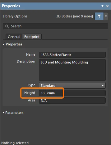
Height design rules can be defined during board design (click Design » Rules in the PCB Editor), typically testing for maximum component height in a class of components or within a room definition.
A better option for defining height information would be to attach 3D Bodies to the PCB footprint.
Managing Components With Routing Primitives
When a design is transferred, the footprint specified in each component is extracted from the available libraries and placed on the board. Then each pad in the footprint has its net property set to the name of the net connected to that component pin in the schematic. All objects touching a pad connect to the same net as the pad.
The PCB editor includes a comprehensive net management tool. To launch it select Design » Netlist » Configure Physical Nets from the main menus to open the Configure Physical Nets dialog. Click the Menu button for a menu of options. Click the New Net Name header drop-down to select the net to assign to the unassigned primitives.

Footprints With Multiple Pads Connected to the Same Pin
The footprint shown below, a SOT223 transistor, has multiple pads that are connected to the same logical schematic component pin - Pin 2. To make this connection, two pads have been added with the same designator - '2'. When the Design » Update PCB command is used in the Schematic Editor to transfer design information to the PCB, the resulting synchronization will show the connection lines going to both pads in the PCB editor, i.e. they are on the same net. Both of these can be routed.

SOT223 footprint showing two pads with a designator of 2.
Silkscreen Preparation
To assist in resolving common Design for Manufacture (DFM) issues faced by having silkscreen overlapping exposed copper and holes, the PCB footprint editor includes a dedicated feature for preparing the silkscreen for your footprints. These issues can be effectively addressed by:
-
automated clipping of silkscreen lines and arcs;
-
automated clipping or movement of fills and regions;
-
automated movement of silkscreen text strings.
The silkscreen preparation tool can also be accessed when designing a PCB –
learn more.
To access the silkscreen preparation tool in the PCB footprint editor, use the Tools » Silkscreen Preparation command from the main menus. The Silkscreen Preparation dialog will open.

Use the dialog to configure the settings of the silkscreen object clipping/movement. The available options are:
-
Clip to Exposed Copper – enable to automatically clip objects to exposed copper.
-
Clip to Solder Mask Openings – enable to automatically clip objects to solder mask openings.
-
Silkscreen Clearance – define the minimum acceptable value between silkscreen objects and exposed copper / solder mask openings and holes.
-
Min Remaining Length – if the line/arc length is less than the defined value after clipping, the objects will be removed from the footprint. Note that this length is the vertex-to-vertex length, not the edge-to-edge length –
![]() show image.
show image.
-
Move Text – enable to move silkscreen text strings away from exposed copper / solder mask openings and holes if the distance between them is less than the Silkscreen Clearance. The movement is limited by the Max Distance value.
-
Fill & Region – select an action to be performed for fills and regions when the distance between them and exposed copper / solder mask openings and holes is less than the Silkscreen Clearance:
-
None – fills and regions remain untouched.
-
Clip – fills and regions will be clipped to maintain the Silkscreen Clearance. Fills are converted to regions if applicable.
-
Move – fills and regions will be moved away from exposed copper / solder mask openings and holes. The movement is limited by the Max Distance value.
-
Max Distance – define a maximum distance to which text strings, component designators, fills and regions can be moved to maintain the Silkscreen Clearance.
Click OK to perform clipping and/or movement of silkscreen objects according to the settings in the dialog.
If an action cannot be performed for an object (e.g., a text string cannot be moved due to the limitation of Max Distance), a message for this object will appear in the Messages panel.
An example of the silkscreen preparation tool performance is shown below.
Creating a Footprint Using the IPC Compliant Footprint Wizard
The IPC Compliant Footprint Wizard generates a PCB footprint that is truly compliant with Revision B of the IPC standard 7351 - Generic Requirements for Surface Mount Design and Land Pattern Standard. Rather than working directly from footprint dimensions (as the Footprint Wizard does), the IPC Compliant Footprint Wizard uses dimensional information from the component itself, and then calculates suitable pad and other footprint properties in accordance with the algorithms released by the IPC.
Instead of requiring you to enter the properties of the pads and tracks that are used to define the footprint, the Wizard takes the actual component dimensions as its inputs. Based on the formulas developed for the IPC-7351 standard, the Wizard then generates the footprint using standard Altium Designer objects, such as pads and tracks.
This dialog is compliant with Revision B of the IPC standard 7351 - Generic Requirements for Surface Mount Design and Land Pattern Standard. IPC-7351B was released in 2010 and supersedes IPC-7351A (which was released in 2007).

To access the IPC Compliant Footprint Wizard in Altium Designer, the IPC Footprint Generator software extension must be installed. This extension is installed with Altium Designer by default. It can be installed or removed manually.
For more information about managing extensions, refer to the Extending Your Installation page (Altium Designer Develop, Altium Designer Agile, Altium Designer).
To run the IPC Compliant Footprint Wizard, select Tools » IPC Compliant Footprint Wizard from the main menus in a PCB Library document.
On the Select Component Type page, choose the family of components for which you want to create a footprint on the Select Component Type page. The preview region on the right-hand side of the Wizard dynamically changes to show the currently selected component and also states the type of packages that are allowed to be generated. The following table lists the component types and packages that are supported in the Wizard.
| Name |
Description |
Included Packages |
| BGA |
Ball Grid Array |
BGA, CGA |
| BQFP |
Bumpered Quad Flat Pack |
BQFP |
| CAPAE |
Electrolytic Aluminum Capacitor |
CAPAE |
| CFP |
Ceramic Dual Flat Pack - Trimmed and formed Gullwing Leads |
CFP |
| Chip Array |
Chip Array |
Chip Array |
| DFN |
Dual Flat No-lead |
DFN |
| CHIP |
Chip Components, 2-Pins |
Capacitor, Inductor, Resistor |
| CQFP |
Ceramic Quad Flat Pack - Trimmed and formed Gullwing Leads |
CQFP |
| DPAK |
Transistor Outline |
DPAK |
| LCC |
Leadless Chip Carrier |
LCC |
| LGA |
Land Grid Array |
LGA |
| MELF |
MELF Components, 2-Pins |
Diode, Resistor |
| MOLDED |
Molded Components, 2-Pins |
Capacitor, Inductor, Diode |
| PLCC |
Plastic Leaded Chip Carrier, Square - J Leads |
PLCC |
| PQFN |
Pullback Quad Flat No-Lead |
PQFN |
| PQFP |
Plastic Quad Flat Pack |
PQFP, PQFP Exposed Pad |
| PSON |
Pullback Small Outline No-Lead |
PSON |
| QFN |
Quad Flat No-Lead |
QFN, LLP |
| QFN-2ROW |
Quad Flat No-Lead, 2 Rows, Square |
Double Row QFN |
| SODFL |
Small Outline Diode, Flat Lead |
SODFL |
| SOIC |
Small Outline Integrated Package, 1.27mm Pitch - Gullwing Leads |
SOIC, SOIC Exposed Pad |
| SOJ |
Small Outline Package - J Leads |
SOJ |
| SON |
Small Outline Non-Lead |
SON, SON Exposed Pad |
| SOP, TSOP |
Small Outline Package - Gullwing Leads |
SOP, TSOP, TSSOP |
| SOT143/343 |
Small Outline Transistor |
SOT143, SOT343 |
| SOT223 |
Small Outline Transistor |
SOT223 |
| SOT23 |
Small Outline Transistor |
3-Leads, 5-Leads, 6-Leads |
| SOT89 |
Small Outline Transistor |
SOT89 |
| SOTFL |
Small Outline Transistor, Flat Lead |
3-Leads, 5-Leads, 6-Leads |
| WIRE WOUND |
Precision Wire Wound Inductor, 2-Pins |
Inductor |
The subsequent pages of the Wizard change depending on the component type selected. Follow the Wizard's intuitive pages to set up the particular component footprint as required. Some notes on working with the IPC Compliant Footprint Wizard:
Creating a Footprint Using the Footprint Wizard
The PCB footprint editor includes a Footprint Wizard. This Wizard allows you to select from various package types and fill in appropriate information and it will then build the component footprint for you. Note that in the Footprint Wizard, you enter the sizes required for the pads and component overlay.

To launch the Footprint Wizard, select Tools » Footprint Wizard from the main menus or right-click in the design space and choose the Tools » Footprint Wizard command from the context menu.
Use the Component patterns page to specify the pattern of the component you want to create. Select the desired pattern from the list then use the drop-down to select the unit for the component (Imperial (mil) or Metric (mm)). Available patterns are:
-
Ball Grid Arrays (BGA)
-
Capacitors
-
Diodes
-
Dual In-line Packages (DIP)
-
Edge Connectors
-
Leadless Chip Carriers (LCC)
-
Pin Grid Arrays (PGA)
-
Quad Packs (QUAD)
-
Resistors
-
Small Outline Packages (SOP)
-
Staggered Ball Grid Arrays (SBGA)
-
Staggered Pin Grid Arrays (SPGA)
The subsequent pages of the Wizard change depending on the component pattern selected. Follow the Wizard's intuitive pages to set up the particular component footprint as required.
When setting up the pad naming style for a footprint of the
Edge Connectors,
Leadless Chip Carriers (LCC) or
Quad Packs (QUAD) pattern, click the green arrow to change the naming order/direction –
![]() show image
show image.
Generating a Component Report
To generate a report for the active PCB footprint, choose the Reports » Component command from the main menus. After launching the command, the report will be generated (<PCBLibraryDocumentName>.CMP) in the same folder as the source PCB library document and will automatically be opened as the active document in the main design window. The report lists information including footprint dimensions and a breakdown of the primitive objects that constitute the footprint and the layers on which they reside.
The report will be added to the Projects panel as a free document under the Documentation\Text Documents sub-folder.
