Schematic diagrams are more than just simple drawings – they contain electrical connectivity information about the circuit. You can use this connectivity awareness to validate your design.
Schematic Validation and Configuring the Validation Options
To validate your design, choose the Validate PCB Project <ProjectName> command from the main Project menu. To validate the project focused in the Projects panel, you can also use the Validate Project command from the right-click menu of the project's entry or the  control at the top of the panel.

Validate your design using the Validate PCB Project <ProjectName> command.
The software checks for logical, electrical, and drafting errors between the Unified Data Model and project checking settings. If validation errors and warnings are enabled for display on the schematic (enabled on the Schematic – Compiler page of the Preferences dialog), an offending object will display a colored squiggle beneath it. Hovering over the object will display a pop-up hint that summarizes the violation. A notification is also displayed in the Messages panel.
Use the controls associated with the
Object Hints entry in the
Connectivity Insight Options region (the
System – Design Insight page of the
Preferences dialog) to determine the launch style for object hints (
Mouse Hover and/or
Alt+Double Click).
There are a large number of drafting and electrical checks that can be performed on the validated design. These are configured as part of the project options. Select the Project » Project Options command from the main menus to open the Project Options dialog. The default settings will not suit every design and, therefore, it is important to become familiar with the options and how to configure them to suit your design.
When working with a Workspace project, note that the Workspace's Web Viewer includes the Electrical Rule Check report for the current project. This provides convenient access to ERC violations for review purposes without the need to access the design in Altium Designer. Learn more about DRC and ERC reports in the Web Viewer (
Altium 365 Workspace,
Enterprise Server Workspace).
Drafting Checks
During validation, common drafting and editing errors are checked in accordance with the settings on the Error Reporting tab of the Project Options dialog. The error checks are organized in groups, for example, Violations Associated with Nets, Violations Associated with Components, etc. The groups are listed alphabetically in the dialog. The Report Mode of each violation can be changed to one of four values by clicking on it and selecting the desired value in the drop-down.

Configure the required error checks on the Error Reporting tab of the Project Options dialog. Click within the Report Mode cell of a violation to change it for this violation.
Generally, it is better to first validate the design and examine the warnings with the default settings. For those warnings that are not an issue for the current design, the reporting level can be changed.
See the PCB Design Violation Types section below for detailed information about each error check.
Connectivity Checks
The electrical connectivity is checked in accordance with the settings on the Connection Matrix tab of the Project Options dialog.

The Connection Matrix defines which electrical conditions are allowed and which are not allowed.
The matrix provides a mechanism to establish connectivity rules between component pins and net identifiers, such as Ports and Sheet Entries. It defines the logical or electrical conditions that are to be reported as warnings or errors. For example, an output pin connected to another output pin would normally be regarded as an error condition, but two connected passive pins would not.
Click on the small square in the matrix to change a particular rule. Each rule determines the reporting level for a given pin/net identifier combination. There are four possible values for each rule: Fatal Error, Error, Warning, and No Report.
The Error Reporting and Connection Matrix settings must be examined and set to suit the requirements of the current project.
Interpreting Messages and Locating Errors
When the project is validated, every condition that generates a warning or error is listed in the Messages panel. Note that the Messages panel will only open automatically if there is at least one Error or Fatal Error condition. To check for a Warning, you will need to open the panel manually by clicking the Panels button on the bottom-right of the design space then choose Messages. Once the project has been validated, the panel will list any warnings and errors that have been detected.

The Messages panel displays the warnings and errors detected in the project.
The Messages panel is command central for presenting violations. Things to be aware of include:
-
The Messages panel has two regions – the upper grid region summarizes the warnings/errors; the lower region gives details of the currently selected warning/error.
-
Double-click on a message to cross-probe to that warning/error. Double-click on a detail to show that specific object.
When you double-click on an error in the Messages panel:
-
The schematic zooms to present the object in error. The Zoom Precision is set by the upper slider in the Highlight Methods section of the System – Navigation page of the Preferences dialog.
-
The entire schematic fades except for the object in error. The amount that the schematic fades is controlled by the Dimming level, set by the lower slider in the Highlight Methods section of the System – Navigation page of the Preferences dialog. Click anywhere on the schematic to clear the dimming.

-
You can click on any of the Messages panel column headings (e.g., Class, Document, Message) to assist in sorting the errors and warnings.
-
Right-click in the Messages panel then use the Group By sub-menu options to group the errors and warnings by a specific criteria.
-
Right-click in the Messages panel then use the appropriate Clear command to delete messages or use the Export To Report command to export the messages to a report.
Clearing messages does not necessarily mean the messages have been resolved. The same unresolved messages will be listed after performing validation again. Message clearance is a visual aid when resolving errors in the design that allows you to manually remove messages as you feel they have been resolved. Validation must be launched again to obtain an up-to-date picture of any violations that still exist.
-
The panel includes warnings and errors detected from settings in both the Error Reporting tab and the Connection Matrix tab.
-
When you right-click on a warning/error in the Messages panel then select the Place Specific No ERC for this violation command, you will automatically cross-probe to the error location and a No ERC directive will appear on the cursor, ready to place on the error location to suppress error checks. Learn more about Suppressing ERC Violations.
Resolving a Warning or Error
It is important to address each warning or error that is detected. The default error settings tend to be conservative since it is better for the software to err on the side of being cautious and let you decide if the testing boundaries can be relaxed. For example, your design may require IO pins to be connected to Input ports, requiring you to adjust the appropriate cell in the Connection Matrix tab. Another common error check to be changed is the Nets with no driving source, requiring you to disable that check in the Error Reporting tab.
There will be situations when you want to test the entire design for a certain condition, but you want to ignore a warning/error at a specific point in the circuit. For example, you might want to allow a net to be renamed at a specific location, but only in that location. This can be done by placing a No ERC directive at that location.
Suppressing ERC Violations
When you need to allow a specific point in the circuit to not report an error, place a No ERC (Electrical Rules Check) directive on that point meaning do not flag a warning/error at this location. Use a No ERC directive to deliberately limit error checking at a certain point in the circuit that you know will generate a warning (such as an unconnected pin) while still performing a comprehensive check of the rest of the circuit.
The No ERC directive supports a number of different styles and can be displayed in any color. Use this ability to reflect the design intent for this point in the circuit.

Choose a No ERC style that best reflects its function at that point in the circuit.
The No ERC directive has two modes of operation:
-
Suppress All Violations – in this mode, all possible warnings and/or error conditions are suppressed. The directive is often referred to as a Generic No ERC directive, in this mode.
-
Suppress Specific Violations – in this mode, only the selected warnings or error conditions are suppressed; any other warnings or errors will be detected and reported. The directive is often referred to as a Specific No ERC directive, in this mode.
Suppressed violations can be displayed in the
Messages panel by enabling the
Report Suppressed Errors in Messages Panel option, on the
Error Reporting tab of the
Project Options dialog. This feature can be used in the final stages of design to ensure that no critical errors have been inadvertently suppressed.
Note that No ERC directives cannot be used to suppress all types of error checks. When the
No ERC dialog is in the
Violation Types mode, it displays a list of the violation types that can be suppressed. Use this as a guide to learn which error tests can be suppressed.
Example Usage
How many times have you encountered a warning about a net 'not having a driving source', only to find that the message can be safely ignored? Perhaps an input pin is fed from a connector, the pin of which is nominally passive and the driving signal only present when an external cable is plugged in? Maybe the net is sourced from a pull-up resistor or switch, again passive in nature? One of the following strategies could be adopted to resolve this warning:
-
You could change the electrical characteristic of a source pin on the net. This is a fix rather than suppression, but as it involves a change to a pin's default mode of operation, it could create trouble further down the track. For example, consider wiring changes made to a design, in which the graphical display of pin direction is not enabled. Such changes might result in an output being connected to a pin of a passive device. If the pin of that device has been set electrically as an output (to alleviate previous driving source warnings), then you will have created a connection violation.
-
You could set the report mode for the associated violation check – defined on the Error Reporting tab of the Options For Project dialog – to No Report. This disables the check of this particular violation, but you would also not be able to catch any genuine errors elsewhere in the design.
-
The third (and arguably best) option is to place a No ERC directive on the net. You are not changing the design in any way, other than to suppress warning message 'noise' that you know is not a problem.

Place No ERC directives on nets you know will cause 'no driving source' warnings.
Placing a No ERC Directive
A No ERC directive can be placed into a schematic document in a number of ways:
-
Place a generic No ERC directive by choosing the Place » Directives » Generic No ERC command from the main menus, by clicking the
 button on the Wiring toolbar, or by right-clicking in the design space, and selecting Place » Directives » Generic No ERC command.
-
Place a specific No ERC directive on a point in the circuit that is already showing a violation, by right-clicking over a violating object in the design space (highlighted by a wavy colored line) and choosing the Place NoERC to Suppress command, from the context menu.

Using the right-click context menu to place a specific No ERC directive.
-
Place a specific No ERC directive on a point in the circuit that is already showing a violation, by right-clicking on a warning/error in the Messages panel, choosing the Place Specific No ERC for this violation command, then jumping straight to that point in the schematic and placing a No ERC directive configured to suppress that warning/error.

Using the right-click context menu in the Messages panel to place a specific No ERC directive.
The command will only be available if the message is a Net-related compiler violation.
Editing a No ERC Directive
During placement, and while the No ERC object is still floating on the cursor, the following editing actions can be performed:
-
From the Properties panel. This method of editing uses the associated Properties panel mode to modify the properties of an object.

The No ERC mode of the Properties panel
During placement, the No ERC mode of the Properties panel can be accessed by pressing the Tab key.
After placement, the No ERC mode of the Properties panel can be accessed in one of the following ways:
-
Double-click on the placed directive.
-
Placing the cursor over the directive then right-click and choose Properties from the context menu.
-
If the Properties panel is already active, select the directive.
The properties can be accessed prior to entering placement mode from the
Schematic – Defaults page of the
Preferences dialog. This allows the default properties for the object to be changed, which will be applied when placing subsequent objects.
-
From the No ERC dialog. This method of editing uses the No ERC dialog to modify the violation types and connection errors of a Specific No ERC object.
 and Connection Matrix mode (the second image)")
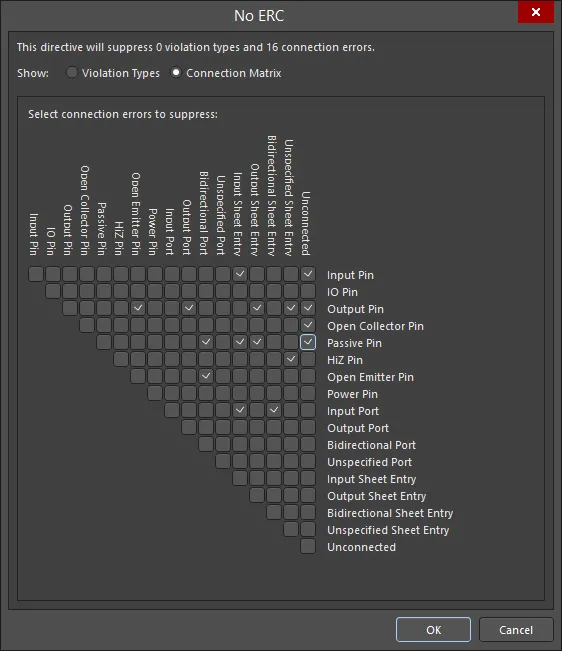
The No ERC dialog showing Violation Types mode (the first image) and Connection Matrix mode (the second image)
The dialog can be accessed by clicking Specific Violations in the Suppressed Violations region of the Properties panel in No ERC mode (mentioned above).

Options and Controls of the No ERC Dialog
-
Top statement - This statement allows you to quickly see how many violation types and connection errors are currently suppressed. The statement is updated as you make changes in the dialog.
-
Show - select either Violation Types or Connection Matrix to view and configure the respective No ERC directive.
Violation Types
This mode allows you to suppress or unsuppress violation types.
-
Violation Type To Suppress - displays a list of the violation types available to configure.
-
Report Mode - displays the current report mode for the listed violation type.
-
Suppress - check the box to suppress the associated violation type; uncheck to unsuppress.
Right-click Menu
The [xxx] in the following right-click menu commands will change dependent upon the violation type that was selected (or the cursor was hovered over) when the right-click was performed.
You also can right-click on a Violations Associated with entry to access right-click menu commands for that entire object.
-
Suppress only "[xxx]" - use to suppress only those violations types listed within the quotes.
-
Unsuppress only "[xxx]" - use to unsuppress only those violations types listed within the quotes.
-
Suppress All "[xxx]" - use to suppress all violations types of the object listed within the quotes.
-
Unsuppress All "[xxx]" - use to unsuppress all violations types of the object listed within the quotes.
-
Suppress All - use to suppress all listed violation types regardless of the object or cursor placement.
-
Unsuppress All - use to unsuppress all listed violation types regardless of the object or cursor placement.
-
Toggle All - use to toggle the Suppress checkbox of all violation types.
Connection Matrix
This mode allows you to suppress or unsuppress connection errors.
-
Grid - use the checkboxes in the grid to suppress (checked) or unsuppress (unchecked) the desired connection errors.
As you hover over a checkbox, the checkbox and corresponding connections are highlighted in bold, which makes updating the desired connection errors easier to update.
Right-click Menu
The [xxx] in the following right-click menu commands will change dependent upon the connection error that was selected (or the cursor was hovered over) when the right-click was performed.
-
Suppress only "[xxx]" - use to suppress only those connection errors listed within the quotes.
-
Unsuppress only "[xxx]" - use to unsuppress only those connection errors listed within the quotes.
-
Suppress All "[xxx]" - use to suppress all connection errors within the quotes. There are two of these commands, one for each part of the connection.
-
Unsuppress All "[xxx]" - use to unsuppress all connection errors within the quotes. There are two of these commands, one for each part of the connection.
-
Suppress All - use to suppress all connection errors in the grid.
-
Unsuppress All - use to unsuppress all connection errors in the grid.
-
Toggle All - use to toggle the checkbox of all connection errors. Checked boxes will be unchecked; unchecked boxes will be checked.
The Specific No ERC directive can be configured to target multiple violations to support circuits that will generate multiple errors/warnings.
-
From the SCH List and SCH Filter panels. A List panel allows you to display design objects from one or more documents in tabular format, enabling quick inspection and modification of object attributes. Used in conjunction with appropriate filtering – by using the applicable Filter panel or the Find Similar Objects dialog – it enables the display of just those objects falling under the scope of the active filter – allowing you to target and edit multiple design objects with greater accuracy and efficiency.

A Generic No ERC directive can be quickly switched to be a Specific No ERC directive, and vice-versa, either through the Properties panel (in the Suppressed Violations section), or by toggling the Suppress Specific Violations property, on the SCH List panel.
Deactivating a No ERC Directive
Rather than deleting a No ERC directive, it can be made inactive (disabled in the eyes of validation). This state can be changed by toggling the directive's Active property – available through any of the methods of editing. An inactive No ERC directive will appear gray in the design space.

If you need to temporarily remove use of a No ERC directive, render it inactive, rather than deleting it.
Controlling the Printing of No ERC Directives
By default, No ERC markers are included during printing. To control this by either disabling their inclusion entirely or excluding only specific symbols, use the Print dialog as shown below.

Control the printing of No ERC markers in the Print dialog.
No ERC
 Use No ERC markers to suppress error/warning messages about a specific node in the circuit.
Summary
The No ERC object is a design directive. It is placed on a node in the circuit to suppress all reported Electrical Rule Check warnings and/or error violation conditions that are detected when the schematic project is compiled. Use No ERC to deliberately limit error checking at a certain point in the circuit that you know will generate a warning (such as an unconnected pin) while still performing a comprehensive check of the rest of the circuit.
The No ERC directive supports a number of different styles and can be displayed in any color. Use this ability to reflect the design intent for this point in the circuit.
Choose a No ERC style that best reflects its function at that point in the circuit.
The No ERC directive has two types:
-
All Violations – all possible warnings and/or error conditions are suppressed.
-
Specific Violations – only the selected warnings or error conditions are suppressed; any other warnings or errors will be detected and reported.
Availability
No ERC design directives are available for placement in the Schematic Editor only. To place a No ERC directive:
-
Click Place » Directives » Generic No ERC from the main menus to place a No ERC marker that is pre-configured to target all violations. This is sometimes referred to as a Generic No ERC directive.
-
Right-click in the schematic editor then click Place » Directives » Generic No ERC.
Placement - Generic No ERC Directive
After launching the command, the cursor will change to a cross-hair and you will enter placement mode. Perform the following to place the No ERC directive:
-
Position the cursor over a wire or other net object then click Enter to place a directive at that point in the circuit.
-
Continue placing further No ERC directives or right-click or press Esc to exit placement mode.
Additional actions that can be performed during placement are:
-
Press the Tab key to pause the placement and access the No ERC mode of the Properties panel, from where its properties can be changed on-the-fly. Click the design space pause button overlay to resume placement.
While attributes can be modified during placement (
Tab to access the
Properties panel), keep in mind that these will become the default settings for further placement unless the
Permanent option on the
Schematic – Defaults page of the
Preferences dialog is enabled. When this option is enabled, changes made will affect only the object being placed and subsequent objects placed during the same placement session.
Graphical Editing
The No ERC marker cannot be modified graphically other than changing its location. To move a No ERC marker, click and hold while dragging it to a new location.
If attempting to graphically modify an object that has its Locked property enabled, a dialog will appear asking for confirmation to proceed with the edit. If the Protect Locked Objects option is enabled on the Schematic – Graphical Editing page of the Preferences dialog, and the Locked option for that design object is enabled as well, then that object cannot be selected or graphically edited. Click the locked object to select it then disable the Locked property in the List panel or disable the Protect Locked Objects option to graphically edit the object.
Non-Graphical Editing
The following methods of non-graphical editing are available.
Editing via the No ERC Dialog or Properties Panel
Panel page: No ERC Properties
This method of editing uses the associated No ERC dialog and the Properties panel mode to modify the properties of an object.

 The No ERC dialog (first image) and the No ERC mode of the Properties panel (second image)
After placement, the No ERC dialog can be accessed by:
-
Double-clicking on the placed No ERC object.
-
Placing the cursor over the No ERC object, right-clicking then choosing Properties from the context menu.
During placement, the No ERC mode of the Properties panel can be accessed by pressing the Tab key. Once the No ERC is placed, all options appear.
After placement, the No ERC mode of the Properties panel can be accessed in one of the following ways:
-
If the Properties panel is already active, by selecting the No ERC object.
-
After selecting the No ERC object, select the Properties panel from the Panels button in the bottom right section of the workspace, or by select View » Panels » Properties from the main menu.
If the
Double Click Runs Interactive Properties option is disabled (default) on the
Schematic - Graphical Editing page of the
Preferences dialog, when the primitive is double-clicked or you right-click on a selected primitive then choose
Properties, the dialog will open. When the
Double Click Runs Interactive Properties option is enabled, the
Properties panel will open.
While the options are the same in the dialog and the panel, the order and placement of the options may differ slightly.
The properties can be accessed prior to entering placement mode from the
Schematic – Defaults page of the
Preferences dialog. This allows the default properties for the object to be changed, which will be applied when placing subsequent objects.
Editing via an Associated Properties Dialog
This method of editing uses the No ERC dialog to modify the violation types and connection errors of a Specific No ERC object.
 and Connection Matrix mode (second image)")
 The No Erc dialog showing Violation Types mode (first image) and Connection Matrix mode (second image)
The dialog can be accessed by clicking Specific Violations in the Suppressed Violations region of the No ERC dialog and the Properties panel in No ERC mode.
The Specific No ERC directive can be configured to target multiple violations to support circuits that will generate multiple errors/warnings.
Editing Multiple Objects
The Properties panel supports multiple object editing, where the property settings that are identical in all currently selected objects may be modified. When multiples of the same object type are selected manually, via the Find Similar Objects dialog or through a SCH Filter or SCH List panel, a Properties panel field entry that is not shown as an asterisk (*) may be edited for all selected objects.

Editing via a List Panel
Panel pages: SCH List, SCH Filter
A List panel allows you to display design objects from one or more documents in tabular format, enabling quick inspection and modification of object attributes. Used in conjunction with appropriate filtering - by using the applicable Filter panel or the Find Similar Objects dialog - it enables the display of just those objects falling under the scope of the active filter – allowing you to target and edit multiple design objects with greater accuracy and efficiency.
No ERC Properties
Schematic Editor object properties are definable options that specify the visual style, content and behavior of the placed object. The property settings for each type of object are defined in two different ways:
-
Pre-placement settings – most No ERC object properties, or those that can logically be pre-defined, are available as editable default settings on the Schematic - Defaults page of the Preferences dialog (access from the
 button at the top-right of the design space). Select the object in the Primitive List to reveal its options on the right.

-
Post-placement settings – all No ERC object properties are available for editing in the No ERC dialog and the Properties panel when a placed No ERC is selected in the design space.

If the
Double Click Runs Interactive Properties option is disabled (default) on the
Schematic - Graphical Editing page of the
Preferences dialog, when the primitive is double-clicked or you right-click on a selected primitive then choose
Properties, the dialog will open. When the
Double Click Runs Interactive Properties option is enabled, the
Properties p
anel will open.
While the options are the same in the dialog and the panel, the order and placement of the options may differ slightly.
In the below properties listing, options that are not available as default settings in the Preferences dialog are noted as "Properties panel only".
Location (Properties panel only)
-
(X/Y)
-
X (first field) - the current X (horizontal) coordinate of the reference point of the object, relative to the current design space origin. Edit to change the X position of the object. The value can be entered in either metric or imperial; include the units when entering a value whose units are not the current default.
-
Y (second field) - The current Y (vertical) coordinate of the reference point of the object, relative to the current origin. Edit to change the Y position of the object. The value can be entered in either metric or imperial; include the units when entering a value whose units are not the current default.
-
Rotation - use the drop-down to select the rotation.
Properties
-
Color - click on the colored box to access a drop-down from which you can select the default color.
-
Symbol - use the drop-down to select the default from the available choices.
-
Active - enable to make the primitive active.
Suppressed Violations (Properties panel only)
-
All Violations - select to display all violations for this object. The Violation Type and Report Mode for the violations are displayed in the grid.
-
Specific Violations - select to display specific violations for this object. The Violation Type and Report Mode for the violations are displayed in the grid.
-
Add - click to open the No ERC dialog to add a new violation. After clicking OK, the new violation will be added to the grid. Click
 to remove the currently selected violation.
PCB Design Violation Types
Violations Associated with Buses
Bus indices out of range
This violation occurs when the index of a constituent net connected to a bus lies outside the range specified by the net to which the bus is associated.
Notification in the Messages Panel
A notification is displayed in the Messages panel in the following format:
Bus index out of range on <NetPrefix> Index = <NetIndex>
where:
-
NetPrefix is the prefix of the constituent net connected to the bus (e.g., A for net A8, connected to a bus associated to net A[0..7]).
-
NetIndex is the erroneous index of the constituent net (e.g., net A8 has an index of 8).
Recommendation for Resolution
Either amend the index of the offending net so that it lies within the correct range, or rename the net altogether. The latter would be typical if you have named the net by mistake and it is not a constituent of the net transported by the bus object.
Bus range syntax errors
This violation occurs when the syntax of the net to which the bus is associated is specified incorrectly.
Notification in the Messages Panel
A notification is displayed in the Messages panel in the following format:
Bus range syntax error <NetName> at <Location>
where:
-
NetName is the name of the parent net to which the offending bus object is associated.
-
Location is the X, Y coordinates for the offending bus object's electrical hotspot.
Recommendation for Resolution
Correctly define bus syntax of the offending net identifier (e.g., net label, port, sheet entry, etc.). The correct syntax should appear in one of the following formats:
-
NetName[LowerIndex..UpperIndex]
-
NetName[UpperIndex..LowerIndex]
For example, consider a bus that carries two constituent nets, A0 and A1. The bus syntax in this case should be A[0..1] or A[1..0]. Examples of incorrect syntax would include: A[0.1], A[1-0], A[0,1], A[..1], and A[0..].
Illegal bus range values
This violation occurs when at least one index in the syntax for a net associated with a bus is negative in value.
Notification in the Messages Panel
A notification is displayed in the Messages panel in the following format:
Illegal bus range value <BusLabel> at <Location>
where:
-
BusLabel is the defined bus labeling where the illegal value has been detected.
-
Location is the X, Y coordinates for the offending bus object's electrical hotspot.
Recommendation for Resolution
Correctly define bus syntax of the offending net identifier (e.g., net label, port, sheet entry, etc.). The correct syntax should appear in one of the following formats:
-
<NetName>[<LowerIndex>..<UpperIndex>]
-
<NetName>[<UpperIndex>..<LowerIndex>]
LowerIndex and UpperIndex can be zero or a positive integer, but cannot be negative in value.
Mismatched bus label ordering
This violation occurs when two net identifiers associated with the same bus slice define bus labels with ordering that is not in the same direction (ascending or descending).
Notification in the Messages Panel
A notification is displayed in the Messages panel in the following format:
Mismatched bus ordering on <NetName> Low value first and High value first
where:
-
NetName is the name of the parent net to which the mismatched bus ordering is associated.
Recommendation for Resolution
Identify the net identifiers (port, net label, sheet entry, etc.) whose bus ordering is not consistent. Determine the correct ordering and amend the naming for the erroneous object.
Mismatched bus widths
This violation occurs when two net identifiers associated with the same bus slice define bus labels with differing widths. For example, a port, with the name A[0..7], might be connected to a bus whose attached net label is defined as A[0..15].
Notification in the Messages Panel
A notification is displayed in the Messages panel in the following format:
Mismatched bus widths on bus section <NetName> (<BusSize1> and <BusSize2>)
where:
-
NetName is the name of the parent net to which the mismatched bus objects are associated.
-
BusSize1 is the width of the first of the offending bus objects.
-
BusSize2 is the width of the second of the offending bus objects.
Recommendation for Resolution
Identify the net identifiers (port, net label, sheet entry, etc.), the bus label widths of which are not consistent. Determine the correct width and amend the naming for the erroneous object.
Mismatched Bus/Wire object on Wire/Bus
This violation occurs when a wire object is incorrectly connected to a bus, or a bus object is incorrectly connected to a wire. For example, port A might be connected to a bus, but the correct bus label syntax (e.g., A[0..1]) has not been entered for the port's name. In effect, the port is a single signal (or wire) object that is now erroneously connected to a bus.
Notification in the Messages Panel
A notification is displayed in the Messages panel in the following format:
<ObjectIdentifier> at <Location> placed on a <ObjectType>
where:
-
ObjectIdentifier represents the mismatched object, which can be either a bus or wire object (e.g., pin, port, power port, net label, off-sheet connector, sheet entry). The identifier will appear in one of the following two formats:
-
For a bus –
Bus <Object> <Name> (e.g. Bus Net Label GND_BUS[..]).
-
For a wire –
Wire <Object> <Name> (e.g. Wire Port TXD).
-
Location is the X,Y coordinates for the object's electrical hotspot.
-
ObjectType is the object on which the offending object has been placed – either a wire or a bus.
Recommendation for Resolution
To resolve the issue, consider the following:
-
Is the connection correct? – should a bus connecting to the object really be a wire and vice versa?
-
Is the object defined correctly? – for a bus object, ensure that the object's name is specified using the correct bus syntax in the form
<Name>[<LowIndex>..<HighIndex>] or <Name>[<HighIndex>..<LowIndex>]. For example, a byte-wide data output port might be specified as DAT_OUT[7..0]. For a wire object, ensure that the object's name defines a single signal and is not defined using bus syntax.
Mixed generic and numeric bus labeling
This violation occurs when two net identifiers (port, net label, sheet entry, etc.,) connected to the same bus slice differ in their bus syntax – one defines a bus range in numeric format (e.g., A[0..2]), while the other defines the range in a generic format (e.g., A[0..b]).
Notification in the Messages Panel
A notification is displayed in the Messages panel in the following format:
Mismatched generic and numeric bus labeling on <NetName> <Level> value first and Generic
where:
-
NetName is the name of the parent net to which the mismatched bus labeling is associated.
-
Level depends on the numeric ordering for the net. If ascending (e.g., [0..2]) Level will appear as Low. If descending (e.g., [2..0]) Level will appear as High.
Recommendation for Resolution
Determine which of the offending objects is erroneous in its bus label specification and change it accordingly.
The use of Generics in bus names is not supported. Ensure that numeric values are used instead.
Violations Associated with Components
Component has been deleted
This violation occurs when at least one component has been deleted from a project design. Operating as a 'soft delete', deleted components are moved to a dedicated Trash location where they can be retrieved (Restore) or completely removed (Permanently Delete) from a deleted entry's menu options (⋯) in the browser interface of the connected Workspace.
Notification in the Messages Panel
A notification is displayed in the Messages panel in the following format:
ComponentName: Component has been deleted
where:
-
ComponentName is the name of the Workspace component.
Recommendation for Resolution
If the component was deleted by mistake, it can be restored by someone with appropriate access rights from the Trash page of the Workspace's browser interface. Otherwise, replace the component used in the design with another equivalent component that is available in the connected Workspace.
Component Implementations with invalid pin mappings
This violation occurs when compiling an Integrated Library Package (*.LibPkg) and the pin mapping between the schematic component and the linked model is found to be invalid.
Notification in the Messages Panel
A notification is displayed in the Messages panel in the following format:
ComponentName: Could not find port <ModelPinNumber> on model <ModelName> for pin <ComponentPinNumber> – PCB model related
ComponentName: Could not map port <ModelPinNumber> on model <ModelName> to a pin – simulation model related
where:
-
ComponentName is the name of the component in the source schematic library.
-
ModelPinNumber is the expected designator for the pin/pad that could not be found on the linked model.
-
ModelName is the name of the model that is linked to the component.
-
ComponentPinNumber is the designator of the pin on the source schematic component to which the erroneous pin of the model is mapped.
Recommendation for Resolution
Resolution involves accessing the mapping between the schematic symbol and the target domain model. To do this, you'll first need to be viewing the properties for the applicable schematic library component. Double-click on the entry for the component in the Components list of the SCH Library panel to access the Properties panel, with the properties for that component loaded.
If the PCB model related violation message is displayed, select the model in the Footprint section of the panel and click the  button underneath the list to access the PCB Model dialog. Once there, click on the Pin Map button to access the Model Map dialog. In the Component Pin Designator column, find the pin number flagged by the message (
ComponentPinNumber). The violation arises because the corresponding entry in the Model Pin Designator column points to a pad designator that does not exist in the PCB model. Amend the entry as required. Typically there will be a one-to-one mapping, with the designators on both sides the same.
If the simulation model related message is displayed, select the model in the Models section of the panel and click the button underneath the list to access the Sim Model dialog. Once there, click on the Port Map tab. This violation will arise when the model pin is not correctly mapped to a pin of the schematic component. This can happen when the entry for the model pin has been set to a pin that is already mapped, or to Not Connected. Amend the entry as required.
Component revision has inapplicable state
This violation occurs when at least one placed instance of a Component Item Revision – placed from a connected Workspace – is detected to be in an inapplicable state. For example, the component is currently Depracated or Obsolete and should therefore have no place on the latest design spin. Applicability is determined through the Allowed to be used in designs option in the State Properties dialog. From within the Edit Lifecycle Definitions dialog, access this dialog for the required state, either by double-clicking on the state's entry within the parent lifecycle definition or by selecting its entry and clicking the edit icon that appears ( ). When this option is enabled, an Item Revision in this state is permitted to be used in a design. It is deemed to be Applicable. If this option is disabled, an Item Revision in this state cannot be validly used and is deemed Inapplicable (or non-applicable).
The
Edit Lifecycle Definitions dialog is itself accessed from the
Data Management – Servers page of the
Preferences dialog, by clicking the
Properties button for the Workspace to which you are actively signed in, then selecting
Lifecycles from the drop-down menu.
Notification in the Messages Panel
A notification is displayed in the Messages panel in the following format:
Component <Designator> <Comment>: Component revision has inapplicable state
where:
-
Designator is the component instance's Designator.
-
Comment is the component instance's Comment.
Recommendation for Resolution
Use the Item Manager dialog to choose a replacement Component Item Revision that is valid for use in the design. Do this for each component that is in an inapplicable state. Alternatively, you can switch out an existing Component Item Revision for a different revision, or revision of a different Component Item at the individual component level. Select the component on the schematic to access its properties through the Properties panel. In the Properties section of the panel, either click the Update button to use the latest revision of the current Component Item, or click the  button at the right of the Design Item ID field to access your Workspace, and browse for another Component Item Revision to use.
Use controls available through the Properties panel or Item Manager dialog to choose a later revision of the Item that is in an applicable state or, if this is not possible (the Item, in general, is not for design use), choose an applicable revision of a different Item.
Notes
-
If a placed component loses connection with its source Workspace – for example, the Workspace from which it was placed is disconnected or you are signed out from your Workspace – it will violate the Component revision has inapplicable state check. This will be reflected in the Messages panel with an entry in the form: Component <Designator> <Comment>: Can't perform revision status validation: Failed to get session: Access denied! User login required for this service.
-
You can also catch components that are being invalidly used within a design during the design release process. Add and configure Component State Checking to your overall release validation regemin.
Component revision is Out of Date
This violation occurs when a component – placed from a connected Workspace – is detected to be out of date.
Notification in the Messages Panel
A notification is displayed in the Messages panel in the following format:
Component <Designator> at <Location>: Component revision is Out of Date
where:
-
Designator is the component instance's Designator.
-
Location is the X, Y coordinates marking the origin of the offending component instance.
Recommendation for Resolution
Use the Item Manager dialog to identify and update components that are not the latest revision. The Item Manager includes a Revision Status column, for any components that are not at the latest revision the component's status will be Out of Date. Select the out-of-date component(s), right-click and choose Update to latest revision from the menu. Once this has been done, Generate an ECO to apply these changes to the affected schematics.
Alternatively, you can switch out an existing Component Item Revision for the latest revision, at the individual component level. Simply select the component on the schematic to access its properties through the Properties panel. In the Properties section of the panel, click the Update button to use the latest revision of the current Component Item.
Note
If a placed component loses connection with its source Workspace – for example the Workspace from which it was placed is disconnected or you are signed out from your Workspace – it will violate the Component revision is Out of Date check. This will be reflected in the Messages panel, with an entry in the form: Component <Designator> <Comment>: Can't perform revision status validation: Failed to get session: Access denied! User login required for this service.
Components containing duplicate sub-parts
This violation occurs when the same part of a multi-part component instance has been placed more than once in a schematic design. For example, you have placed a 74HC32 component with designator U9, but have inadvertently placed two instances of part one of this component, resulting in two instances of U9A in the design.
Notification in the Messages Panel
A notification is displayed in the Messages panel in the following format:
Component <ComponentName> has duplicate sub-parts at <Location1> and <Location2>
where:
-
ComponentName is the name of the offending component in terms of its designator and library reference.
-
Location1 is the X, Y coordinates for the first instance of the particular sub-part.
-
Location2 is the X, Y coordinates for the duplicate instance of the particular sub-part.
Recommendation for Resolution
Change the part number for the offending parts as required, using the Increment Part Number command – available from the main Edit menu or from the Part Actions sub-menu (when right-clicking over the part). The advantage of launching the command from the Edit menu is that you remain in increment mode, allowing you to cycle through the part numbers until you reach the desired one.
Components with duplicate pins
This violation occurs when two or more pins in a component have the same designator.
Notification in the Messages Panel
A notification is displayed in the Messages panel in the following format:
Duplicate pins in component Pin <Identifier1> and Pin <Identifier2>
where:
-
Identifier1 is the identifier for the first instance of the duplicated pin, represented by the part designator-pin designator pairing
-
Identifier2 is the identifier for the second instance of the duplicated pin, represented by the part designator-pin designator pairing.
Recommendation for Resolution
Change the designator of the offending pin(s) accordingly, so that each has a unique assignment. Pin designators can be edited from within the schematic editor for a component that has already been placed:
-
If the component pins are not locked, you can simply select the pin and edit its designator through the Properties panel.
-
Otherwise, edit the pin(s) using the Component Pin Editor dialog. With the component selected in the design space, access to this dialog is made from the Properties panel by clicking the button, below the Pins section, on the Pins tab of the panel.
Typically, the duplication will reside in the library component, in which case you should edit the pin designator for that component in the source schematic library and then pass the change on to placed instances of the component, using the Update From Libraries (Schematic Editor) or Update Schematics (Schematic Library Editor) commands. Both commands are available from the main Tools menus of these editors respectively.
Note
Only one violation instance will be listed in the Messages panel for each distinct component. A component may well have more than two pins with the same designator, but when investigating the violation using the Details region of the panel, only the first two duplicate pins (in alphabetical pin name order) will be listed.
Duplicate Part Designators
This violation occurs when at least two parts across source schematic sheets in a design have the same designator associated with them.
Notification in the Messages Panel
A notification is displayed in the Messages panel in the following format:
Duplicate Component Designators <PartDesignator>
where:
-
PartDesignator is the offending designator.
Recommendation for Resolution
Assign different and unique designators to the duplicates as required. This can be done manually by editing each offending designator or through the use of the Annotate dialog (Tools » Annotation » Annotate Schematics).
Alternatively, reset the duplicate component designators first using the Tools » Annotation » Reset Duplicate Schematic Designators command then use the Tools » Annotation » Annotate Schematics Quietly command to annotate without launching the Annotate dialog.
Generic Component
This violation occurs when a Generic Component has been included in a final design. Generic Components can quickly be placed in a design without the need to find and choose a specific manufacturer part from the available component sources and are intended as placeholders that are easily replaced by a suitable component.
Notification in the Messages Panel
A notification is displayed in the Messages panel in the following format:
Generic Component <PartDesignator> is placed at <Location>
where:
-
Designator is the placed generic component instance's Designator.
-
Location is the X, Y coordinates marking the origin of the offending generic component instance.
Recommendation for Resolution
When a design has progressed to the point where a Generic Component can be replaced with a specific physical component, you may use the Replace Component dialog by selecting the ellipsis menu in the Design Item ID field of the Properties panel. Note this also can be done from the Item Manager or through the project's ActiveBOM document.
Mismatched hidden pin connections
This violation occurs in multi-part components when a hidden pin common to more than one sub-part is connected to different nets.
Notification in the Messages Panel
A notification is displayed in the Messages panel in the following format:
Mismatched hidden pin connections in Pin <Identifier> and Pin <Identifier>
where:
-
Identifier is used to identify the pin in question. The identifier appears in the format PhysicalComponentName-PinDesignator (e.g., U2-7).
Recommendation for Resolution
Reassign the offending pin(s) to the correct nets. A hidden pin is assigned to a net by entering the net name into the Hidden Net Name field in the corresponding List panel (SCHLIB List panel or the SCH List panel) when the panel is displaying pin properties. If this is being done in the SCH List panel, right-click in the panel and enable the Show Children option to list the pins in the panel.
Mismatched pin visibility
This violation is related to the power pins (VCC and GND) of a multi-part component. Typically, these pins are associated with part 0, are automatically connected to the VCC and GND nets for the design, and are hidden. If for one of the component parts, you enable visibility of such a pin, it is no longer connected to the target power net and the error will be flagged.
Notification in the Messages Panel
A notification is displayed in the Messages panel in the following format:
Pin is visible in one sub-part and hidden in another sub-part
Recommendation for Resolution
Either disable the display of the offending power pin(s) in the design space or, if keeping the pins displayed, ensure that a VCC and/or GND power port object is attached to the pin(s) accordingly.
Missing Component Models
This violation occurs when compiling an Integrated Library Package (*.LibPkg) and a linked model for a component in the source schematic library could not be found.
Notification in the Messages Panel
When the linked model is a footprint model or simulation model, a notification is displayed in the Messages panel in one of the following formats:
<ComponentName>: Could not find <ModelName> – when the model search scope is Any.
<ComponentName>: Could not find <ModelName> in <LibraryName> – when the model search scope is Library Name.
<ComponentName>: Could not find <ModelName> in <Path> – when the model search scope is Library Path.
where:
-
ComponentName is the name of the component in the source schematic library.
-
ModelName is the name of the footprint, or simulation model, that is linked to the source component and which could not be found.
-
LibraryName is the name of the library file specified to contain the linked model.
-
Path is the absolute path to a library file specified to contain the linked model.
When the linked model is a signal integrity model, the message is displayed in the Messages panel in the following format:
<ComponentName>: Could not find 'GenericEntity' in <Path>
where:
-
ComponentName is the name of the component in the source schematic library.
-
Path is the absolute path to a library/model.
Recommendation for Resolution
When the problem is a linked footprint or simulation model
This issue is typically caused by one of the following scenarios:
-
The model name is incorrectly specified when defining the model link.
-
The linked model does not reside in the specified library file.
-
The library file containing the linked model has been moved or deleted.
The first port of call in resolving this violation is the associated setup dialog for the model type you are linking to – the PCB Model dialog, or the Sim Model dialog. In each case, check and ensure:
-
The name of the model to which you are linking is correct, and
-
The correct option is used to locate the library/model file in which that model resides.
The format of the displayed error message depends on the search scope you have enabled when locating the model, and can be of great help when tracking down the problem with the model link:
-
If the model could not be found in a specified path (search scope:
Library path), ensure that the library/model file you have specified actually exists at that location and also check the library/model file to see if the model with the specified name exists within.
-
If the model could not be found in a specified library/model file (search scope:
Library name), ensure that the library/model file has been added to the Available Libraries list (Project Libraries, Installed Libraries, Project Search Paths). Also, check to make sure the library/model file contains the model with the same name specified in the link.
-
If the model could simply not be found (search scope:
Any), ensure that a library/model file – containing a model with the same name as that specified in the link – has been added to the Available Libraries list.
When the problem is a linked signal integrity model
Typically caused when the type of signal integrity model (e.g., diode, IC) is not specified, this is resolved in the associated setup dialog for signal integrity models. The easiest way to access this is through the Properties panel when viewing the properties for the selected component. Check that you are using the correct model in the Models section on the General tab of the panel and amend if necessary. The Add and buttons can be used to create a new model (choose Signal Integrity from the list) or modify the existing signal integrity model. This will give access to the Signal Integrity Model dialog, where the Import Ibis button allows pins models to be imported from an Ibis model file.
You can add an Ibis model directly by clicking Add » Ibis model and using the subsequent Ibis Model dialog to define the link to the model and file.
Missing pin found in component display mode
This violation occurs if a missing pin has been detected in one of the display modes for a part.
Notification in the Messages Panel
A notification is displayed in the Messages panel in the following format:
<NumberOfMissingPins> missing pins in <DisplayMode> of design item <DesignItemID>
where:
-
NumberOfMissingPins is the number of missing pins found in the part.
-
DisplayMode is the specific graphical representation mode for the part in which the missing pin(s) has been found. A part has a Normal mode and can have up to 255 defined Alternate modes.
-
DesignItemID is the Design Item ID property of the offending part.
Recommendation for Resolution
This violation typically arises when an alternate graphical mode is defined for a component, but not all pins specified in the Normal mode have been specified for the Alternate (i.e. there must be an identical number of pins between graphical display modes).
In the source schematic library, copy the missing pins from an existing display mode into the offending display mode for the component. This can be performed directly on the schematic sheet for a part that has been placed already, but you would typically tackle the problem from within the library, then push the change across (Tools » Update Schematics).
Sheet Symbol with duplicate entries
This violation occurs when a sheet symbol contains two sheet entries possessing the same name.
Notification in the Messages Panel
A notification is displayed in the Messages panel in the following format:
Sheet Symbol with duplicate entries Sheet Entry <Identifier> at <Location1> and <Location2>
where:
-
Identifier is used to represent the offending sheet entry. The identifier appears in the format SheetSymbolName-SheetEntryName(SheetEntryIOType).
-
Location1 is the X, Y coordinates for the first violating sheet entry.
-
Location2 is the X, Y coordinates for the second violating sheet entry.
Recommendation for Resolution
Change the name of the offending sheet entry object as required, either by editing the name in-situ or by double-clicking on the offending sheet entry and editing its Name in the Properties section of the Properties panel – which presents all properties for the selected sheet entry.
A sheet entry name can also be edited from the
Sheet Entries section on the
General tab of the
Properties panel – when browsing the properties for the selected parent sheet symbol.
Sheet Symbols with duplicated indexes
This violation occurs in a multi-channel design when two or more sheet symbols that reference to the same child schematic sheet and include the Repeat keyword in their Designator fields have common values of channel index ranges.
Notification in the Messages Panel
A notification is displayed in the Messages panel in the following format:
Sheet Symbols <ChannelIdentifier> have duplicated indexes: <ChannelIndexList>
where:
-
ChannelIdentifier is the channel identifier used in the sheet symbols' Designator field.
-
ChannelIndexList is the comma-separated list of channel indexes that are duplicated across offending sheet symbols.
Recommendation for Resolution
Change the designators of offending sheet symbol objects so their index ranges have no common values, either by editing a designator in-situ or by double-clicking on an offending sheet symbol and editing its Designator in the Properties section of the Properties panel – which presents all properties for the selected sheet symbol.
Un-Designated parts requiring annotation
This violation occurs when a component in the design is found to have a default designator (with a ? suffix), i.e. either it has yet to be annotated or the designator has been reset.
Notification in the Messages Panel
A notification is displayed in the Messages panel in the following format:
Un-Designated Part <PartDesignator>
where
-
PartDesignator is the default designator for the un-designated part (e.g. U?, D?, C?, etc).
Recommendation for Resolution
Assign a unique designator to the offending component as required. This can be done manually by editing the designator or through the use of the Annotate dialog (Tools » Annotation » Annotate Schematics).
Alternatively, use the Tools » Annotation » Annotate Schematics Quietly command to annotate without launching the Annotate dialog.
Note
Only one error instance will be listed in the Messages panel for each distinct designator type (U?, D?, C?, etc.). Multiple errors may exist.
Unused sub-part in component
This violation occurs when a part of a multi-part component instance has not been used within the design. For example, three out of four parts for an instance of a 74HC32 component may have been placed and wired but the fourth has not.
This violation does not occur if a part that contains no primitives is not placed in the schematics (provided parts with no primitives are listed below all parts that have primitives in the list of symbol parts that can be seen in the SCH Library panel when editing the symbol in the schematic symbol editor).
Notification in the Messages Panel
A notification is displayed in the Messages panel in the following format:
Component <Identifier> has unused sub-part(s) (<PartNumber>)
where
-
Identifier is the parent component, represented using the format Designator Library Reference (e.g., U11 74HC32)
-
PartNumber is an integer used to indicate which specific part is not being used (e.g., 1 represents part A, 2 represents part B, and so on).
Recommendation for Resolution
Place the unused part and connect its inputs to the ground. To ensure the same root designator, copy an existing part for that component's instance and, after pasting, increment its part number accordingly.
Violations Associated with Documents
Ambiguous Device Sheet Path Resolution
This violation occurs when a target device sheet – specified in the File Name field for a Sheet Symbol – has been found in multiple declared device sheet folders.
Notification in the Messages Panel
A notification is displayed in the Messages panel in the following format:
Ambiguous Device Sheet Resolution for <DeviceSheetName>
where:
-
DeviceSheetName is the current entry for the parent device sheet symbol's File Name field. Unlike the entry in the File Name field, the message includes the extension too (*.SchDoc).
Recommendation for Resolution
Use the Details region of the Messages panel to cross-probe to the device sheet symbol in question. Double-click on the symbol to access its properties through the Properties panel. In the Source section, on the General tab of the panel, the full path to the instance of the device sheet currently being used is displayed.
Remember that the device sheet instance used will be the first detected across declared device sheet folders and that these folders – declared on the Data Management – Device Sheets page of the Preferences dialog – are searched in top-down order. If the currently used device sheet is the correct instance, you can simply ignore this violation. If not, select the folder in which the correct instance exists, and click the Move Up button until that folder is at the top of the list.
Note, however, that while this may solve the immediate issue for this particular device sheet, the ambiguity will still remain. To fully resolve this issue, identify the redundant device sheet(s), and remove it (them) from the other declared device sheet folder(s).
Circular Document Dependency
This violation occurs after using the Create Sheet Symbol From Sheet command from the Design main menu and a schematic document that already is a child in the project is chosen in the Choose Document to Place dialog and the schematic documents chosen have Device Sheet links between each other.
Notification in the Messages Panel
A notification is displayed in the Messages panel in the following format:
Circular dependency between document <DocumentName1> and document <DocumentName2>
where:
-
DocumentName1 and DocumentName2 are the names of the two documents that have Device Sheet links between each other.
Recommendation for Resolution
Review the schematic documents listed in the error message and fix the Device Sheet links between them.
Missing child sheet for sheet symbol
This violation occurs when the link between a sheet symbol and a target schematic sub-document is invalid. This can occur when:
-
A sheet symbol has been placed manually but no sub-level document reference has been entered into the symbol's File Name field.
-
The document reference in the symbol's File Name field has been entered incorrectly – effectively targeting a document that does not exist.
-
The referenced target document has been removed from the project or deleted.
Notification in the Messages Panel
A notification is displayed in the Messages panel in the following format:
Missing child-sheet in <SymbolFileName> in Symbol <SymbolDesignator>
where:
-
SymbolFileName is the current entry for the parent sheet symbol's File Name field.
-
SymbolDesignator is the designator of the parent sheet symbol.
Recommendation for Resolution
Check the entry in the sheet symbol's File Name field in the Properties section on the General tab of the Properties panel (when the sheet symbol is selected in the design space). The target document itself is specified in the Source section (on that same tab of the panel), with the source set to Local for a standard sheet symbol. If the required target document already exists, ensure that the document name (including extension) is entered correctly into the field. If the target document has been removed from the project and you have access to it, add it back in to the project. If the target document does not exist, right-click on the symbol and choose the Create Sheet From Symbol command from the Sheet Symbol Actions sub-menu.
Note
This error is also generated when a Device Sheet Symbol has been placed but the target Device Sheet cannot be found. The target document itself is specified in the Source section on the General tab of the Properties panel (when the device sheet symbol is selected in the design space), with the source set to Device for a device sheet symbol.
Multiple Top-Level Documents
This violation occurs in hierarchical designs when two or more schematic sheets are at the top level of the structure.
Notification in the Messages Panel
A notification is displayed in the Messages panel in the following format:
Multiple top level documents: <SheetName> has been used
where:
-
SheetName is the name of the schematic document currently being used as the top-level sheet.
Recommendation for Resolution
This issue typically arises due to the sheet symbol on the true top sheet not targeting the intended sub-sheet correctly. To resolve this issue, first determine which schematic sheet is the intended sub-sheet. Check to see if a sheet symbol has been placed for the intended sub-sheet on the top-level schematic:
-
If a sheet symbol does not exist, create it – either by manual placement or by using the Design » Create Sheet Symbol From Sheet command from the main menus.
-
If the sheet symbol exists, ensure that it references the sub-sheet. Check the entry in the sheet symbol's File Name field in the Properties section on the General tab of the Properties panel (when the sheet symbol is selected in the design space). The target document itself is specified in the Source section (on that same tab of the panel) with the source set to Local for a standard sheet symbol.
Port not linked to parent sheet symbol
This violation occurs when a port on a child sheet is not matched with a sheet entry on the parent sheet symbol. All sheet entries in the parent sheet symbol must be synchronized (matched) to corresponding ports on the child sheet.
Notification in the Messages Panel
A notification is displayed in the Messages panel in the following format:
Port <PortName> not matched to Sheet-Entry at <Location>
where:
-
PortName is the name of the port on the child sheet.
-
Location is the X, Y coordinates for the port's electrical hotspot.
Recommendation for Resolution
This issue can arise for a number of reasons:
-
The corresponding sheet entry for the port does not exist.
-
The corresponding sheet entry for the port exists but with a different name.
-
The corresponding sheet entry for the port exists but with a different I/O Type.
Use Ctrl+Double Click on the port in question to ascend to the parent sheet symbol. Right-click on the sheet symbol and choose Sheet Symbol Actions » Synchronize Sheet Entries and Ports from the menu that appears. This will open the Synchronize Ports To Sheet Entries dialog for that sheet symbol.
Use the dialog to match the port in question to the required sheet entry. If the sheet entry does not exist, you can create it directly from the dialog. If the sheet entry exists but the Name and/or I/O Type differ, you can determine, as part of the match, whether the Name and I/O Type to be used comes from the port or the sheet entry.
Notes
When the sheet entry and port exist but have different Names and/or I/O Types, there will be a corresponding error message stating that the sheet entry is not matched to a port. Synchronizing the sheet entry with the port will clear both errors.
Sheet Entry not linked to child sheet
This violation occurs when a sheet entry is not matched with a port on the child sheet referenced by the parent sheet symbol. All sheet entries in the parent sheet symbol must be synchronized (matched) to corresponding ports on the child sheet.
Notification in the Messages Panel
A notification is displayed in the Messages panel in the following format:
Sheet-Entry <SheetEntryName> not matched to Port at <Location>
where:
-
SheetEntryName is the name of the sheet entry associated with the parent sheet symbol.
-
Location is the X, Y coordinates for the sheet entry's electrical hotspot.
Recommendation for Resolution
This issue can arise for a number of reasons:
-
The corresponding port for the sheet entry does not exist.
-
The corresponding port for the sheet entry exists but with a different name.
-
The corresponding port for the sheet entry exists but with a different I/O Type.
Right-click on the parent sheet symbol that is parent to the sheet entry in question then choose Sheet Symbol Actions » Synchronize Sheet Entries and Ports from the menu that appears. This will give you access to the Synchronize Ports To Sheet Entries dialog for that sheet symbol.
Use the dialog to match the sheet entry in question to the required port. If the port does not exist, you can create it directly from the dialog. Where the port exists but the Name and/or I/O Type differ, you can determine, as part of the match, whether the Name and I/O Type to be used comes from the sheet entry or the port.
Note
When the sheet entry and port exist but have different Names and/or I/O Types, there will be a corresponding error message stating that the port is not matched to a sheet entry. Synchronizing the sheet entry with the port will clear both errors.
Sheet Names Clash
This violation occurs when the project contains more than one schematic document with the same name in different folders.
Notification in the Messages Panel
A notification is displayed in the Messages panel in the following format:
Project <ProjectName> contains several documents named <SchematicDocumentName>
where:
-
ProjectName is the name of the project associated with the error.
-
SchematicDocumentName is the schematic document that has the same name as other schematic document(s) in the project.
Recommendation for Resolution
Save the offending schematic documents with a different name.
Violations Associated with Harnesses
Conflicting Harness Definition
This violation occurs when there are conflicting Harness Entries for the same Harness Type, either at a graphical or textual level (in the Harness Definition File).
Notification in the Messages Panel
A notification is displayed in the Messages panel in the following format:
Conflicting Harness Definition for <HarnessType>
where:
-
HarnessType is the current conflicting Harness Type.
Recommendation for Resolution
Update the Harness Definition File to reflect the changes, or remove the offending Harness Entry, or change the Harness Type of the offending Harness Entry.
Harness Definition Files for the design can be found in the
Settings\Harness Definitions Files folder for that project, in the
Projects panel.
Harness Connector Type Syntax Error
This violation occurs when either the Harness Type has invalid characters (such as [ ] { } . : ) or if the Harness Type is blank.
Notification in the Messages Panel
A notification is displayed in the Messages panel.
If the Harness Type has invalid characters, this message is displayed in the following format:
Harness Connector Type <HarnessType> should not contain these characters [] {}. :
where:
-
HarnessType is the current conflicting Harness Type.
If the Harness Type is blank, this message is displayed in the following format:
Harness Connector Type cannot be Blank
Recommendation for Resolution
With the offending Harness Connector selected, specify a valid Harness Type in the Properties section of the Properties panel. Ensure the entry does not contain invalid characters.
Invalid Connection to a Harness Connector
This violation occurs when a wire, bus, or signal harness ends inside or is connected to the edge of a harness connector but is not connected to a harness entry.
Notification in the Messages Panel
A notification is displayed in the Messages panel in the following format:
<ObjectType> (<Location1> To <Location2>) ends inside Harness Connector <HarnessType> but it is not connected to any of its Harness Entries
where:
-
ObjectType is the type of the offending object – Net (for a wire), Bus, or Signal Harness.
-
Location1 is the X, Y coordinates for the start point of the offending object.
-
Location2 is the X, Y coordinates for the endpoint of the offending object.
-
HarnessType is the Harness Type of the offending harness connector.
Recommendation for Resolution
Ensure the wire, bus, or signal harness is connected to a harness entry of the harness connector, or edit the wire / bus / signal harness so it does not end inside or is not connected to the edge of a harness connector.
Missing Harness Type on Harness
This violation occurs when a Signal Harness connecting Sheet Entries or connecting a Sheet Entry to a Port is missing a Harness Type.
Notification in the Messages Panel
A notification is displayed in the Messages panel in the following format:
Missing Harness Type on Signal Harness
Recommendation for Resolution
Specify a Harness Type across the Signal Harness for at least one of the objects:
-
Port – specify a Harness Type in the Properties section on the General tab of the Properties panel (which presents all properties for the selected object).
-
Sheet Entry – specify a Harness Type in the Properties section of the Properties panel (which presents all properties for the selected object).
Multiple Harness Types on Harness
This violation occurs when there are multiple Harness Types defined across a Signal Harness.
Notification in the Messages Panel
A notification is displayed in the Messages panel in the following format:
Multiple harness types on harness <HarnessType1>, <HarnessType2>
where:
-
HarnessType1 and HarnessType2 are the multiple Harness Types specified across the Signal Harness.
Recommendation for Resolution
Specify only one Harness Type across the Signal Harness:
-
Port – specify a Harness Type in the Properties section on the General tab of the Properties panel (which presents all properties for the selected object).
-
Sheet Entry – specify a Harness Type in the Properties section of the Properties panel (which presents all properties for the selected object).
-
Harness Connector – specify a Harness Type in the Properties section of the Properties panel (which presents all properties for the selected object).
-
Harness Entry – specify a Harness Type in the Properties section of the Properties panel (which presents all properties for the selected object).
Unconnected Harness Entry
This violation occurs when no wire, bus, or signal harness is connected to harness entry.
Notification in the Messages Panel
A notification is displayed in the Messages panel in the following format:
Unconnected Harness Entry <Identifier>
where:
-
Identifier is used to identify the harness entry in question. The identifier appears in the format HarnessType-HarnessName.
Recommendation for Resolution
Ensure a wire, bus, or signal harness is connected to the harness entry.
Unknown Harness Type
This violation occurs when a Harness Type is found but a matching definition cannot be found in a Harness Definition file. This can happen for one of two reasons:
-
A Signal Harness is connected to an object (Sheet Entry, Port, or Harness Entry) with an unknown Harness Type.
-
When a Harness Entry in a Harness Definition file refers to an unknown Harness Type.
Notification in the Messages Panel
A notification is displayed in the Messages panel in the following format:
Unknown Harness Type <HarnessType>
where:
-
HarnessType is the current unknown Harness Type.
Recommendation for Resolution
Ensure that Sheet Entries, Ports and Harness Entries have a known Harness Type and that Harness Definitions are accurate:
-
Port – specify a Harness Type in the Properties section on the General tab of the Properties panel (which presents all properties for the selected object).
-
Sheet Entry – specify a Harness Type in the Properties section of the Properties panel (which presents all properties for the selected object).
-
Harness Entry – specify a Harness Type in the Properties section of the Properties panel (which presents all properties for the selected object).
Violations Associated with Nets
Adding hidden net to sheet
This violation occurs when there are two or more hidden pins within the project that have the same value entered into their Hidden Net Name property. Hidden pins are sometimes used to define the power pins in a multi-part component. Typically this warning occurs when a library component with hidden pins has been used and the designer was not aware of those hidden pins.
Notification in the Messages Panel
A notification is displayed in the Messages panel in the following format:
Adding hidden net
Recommendation for Resolution
The problem arises when the following properties for the offending pin(s) occur:
-
The Hide option is enabled
-
The Hidden Net Name field contains the specific power net name
If it is by design then the warning can be ignored. Alternatively, you can enable the display of the pin(s) in the design space. This option may prove to be less than desirable, especially if you have many hidden pins connected to power nets. Revealing these pins in the design space can cause clutter as each pin would need to be wired to the appropriate power port object – making the design schematic(s) less easy to read.
If you choose to display the hidden pins and those pins are assigned to Part Zero, they will appear on every part placed in the project. For multi-part component power pins that are not hidden, it can be better to create a separate part in the component just for the power pins.
The Hidden Net Name field is only accessible in the SCHLIB List panel or the SCH List panel. When working with multiple objects, it can be more efficient to edit their properties in the List panel.

Note
Only one instance of this violation type will be listed in the Messages panel. When investigating the error using the Details region of the panel, a single entry will be listed reflecting the net that is being added. There may be multiple nets added – such as GND and VCC – but only one will be listed, determined by alphabetical order. If you clear the violation for a particular net, the next net (in order) will appear under this violation type.
Adding Items from hidden net to net
This violation is related to components and occurs when you have specified one or more pins to be hidden and connected to an existing net within the design – typically a power pin connected to VCC or GND for example.
Notification in the Messages Panel
A notification is displayed in the Messages panel in the following format:
Adding items to hidden net <NetName>
where:
-
NetName is the name of the target net.
Recommendation for Resolution
The problem arises when the following property for the offending pin(s) is evident in the associated Component Pin Editor dialog:
-
The Show option is disabled.
The resolution of this issue is on a per-component basis and also depends on whether a component contains multiple sub-parts.
For a non-multi-part component, enable the display of the pin(s) in the design space (enable the Show option). You will need to wire each pin to the appropriate power port for the net to which you want to connect.
The previous solution can also be applied to multi-part components, but a far better solution is to set the Part Number field to 0. Leave the Show option for the pin disabled. Repeat for each pin that has been connected to a power net in this way. Ideally, the power net connections should be assigned through use of part 0 in the source library component.
Bus Object on a Harness
This violation occurs when a Port, Sheet Entry, or Net Label within a Signal Harness has a name in the form [X..Y] indicating a bus object.
Notification in the Messages Panel
A notification is displayed in the Messages panel in the following format:
Bus <Object> <ObjectName> at <Location> placed on a harness
where:
-
Object is the offending port, sheet entry, or net label.
-
ObjectName is the name of the offending object.
-
Location is the X, Y coordinates for the offending object.
Recommendation for Resolution
Modify the name of the offending object so that it does not use bus syntax.
Differential Pair Net Connection Polarity Inversed
This violation appears when the polarity of a differential pair net is not the same as that of the differential pair pin to which it is connected. For example, the positive net is connected to the negative pin, or vice versa.
Notification in the Messages Panel
A notification is displayed in the Messages panel in the following format:
Inversed connection on differential pair <PairName>: net <NetName> is connected to pin <PinDesignator> (<Polarity>)
where:
-
PairName is the name of the differential pair (e.g. V_TX1).
-
NetName is the name of the offending net (e.g. V_TX1_P).
-
PinDesignator is the designator of the device pin to which the offending net is connected (e.g. E6).
-
Polarity is the polarity of the pin (e.g. negative).
Recommendation for Resolution
Ensure that the net label attached to the connected wire is the same polarity as that of the differential pair pin to which the connection has been made. For example, if the pin name is IO_L02N_0 and the net label is V_TX1_P, change the net label to V_TX1_N.
If a pair of violation messages of this type appears – one for the positive net of the pair attached to the negative pin of the device and one for the negative net of the same pair attached to the positive pin – simply swap the attached net labels around.
Differential Pair Net Unconnected To Differential Pair Pin
This violation appears when a differential pair net is not connected to a differential pair pin of a physical device.
Notification in the Messages Panel
A notification is displayed in the Messages panel in the following format:
Net <NetName> of differential pair <PairName> is not connected to a differential pair pin
where:
-
NetName is the name of the positive or negative polarity net in the pair (e.g. V_RX1_N or V_RX1_P).
-
PairName is the name of the differential pair (e.g. V_RX1).
Recommendation for Resolution
A true differential pair pin is hard-wired for a physical device (e.g., a Xilinx Virtex-II Pro FPGA device). Although such a pin may appear with the identifier N (for negative) or P (for positive) as part of its name, you cannot make a pin differential simply by changing its name.
Consider the following when resolving a violation of this type:
-
If the differential pair net is correct but has been attached/wired to the wrong pin of the device, determine the correct pin and move the net label accordingly.
-
If the differential pair nethas been erroneously specified as a differential pair net, change the associated net label to the correct (non-differential) naming and remove the attached differential pair directive from the connecting wire.
-
If the pin to which the differential pair net is currently connected is, in fact, not to be used at all in the design, ensure that net label, wire, and differential pair directive are removed and place a No ERC marker on it.
Differential Pair Unproperly Connected to Device
This violation appears when a differential pair net is not properly connected to a differential pair pin of a physical device.
Notification in the Messages Panel
A notification is displayed in the Messages panel in the following format:
Misconnected differential pair <PairName>: net <NetName> should be connected to pin <PinDesignator>
where:
-
PairName is the name of the differential pair (e.g., V_TX1).
-
NetName is the name of the positive or negative polarity net in the pair (e.g., V_TX1_N or V_TX1_P).
-
PinDesignator is the designator of the device pin to which the offending net should be connecting (e.g., E6).
Recommendation for Resolution
This type of violation typically arises when the wire object for the differential pair net is not making an electrical connection with the target pin of the device. Ensure proper connection between the wire of the net and the device pin itself.
Duplicate Nets
This violation occurs when two nets with the same name have been detected within the design.
Notification in the Messages Panel
A notification is displayed in the Messages panel in the following format:
Duplicate Net Names <Object> <NetName>
where:
-
Object is either Wire or Bus Slice or Element[n] (for a bus element).
-
NetName is the name of the affected net.
Recommendation for Resolution
When the design data model is being created, nets are created in the following way:
-
Within each sheet, a unique net is created for each set of connected electrical objects.
-
The Net Identifier Scope is then checked to determine if the design is flat or hierarchical.
-
If the design is flat, the sheet-level nets are connected directly between the various sheets.
-
If the design is hierarchical:
-
using the Port attached to the lower-level net, the connectivity is created from that Port up to the Sheet Entry in the Sheet Symbol on the parent sheet, then
-
the connectivity is created between the Sheet Entry and other connected electrical objects on the parent sheet.
To learn more about flat and hierarchical designs, refer to the Creating Circuit Connectivity in Your Schematics page.
This violation can arise when, for example:
-
The design is flat and ports have been used within the design. The Net Identifier Scope is automatically (or manually) set to
Flat (Only ports global). The violation will occur if the same net label has been used between sheets. This is because net labels defined on each sheet, even with the same name, remain local to those sheets. The resolution, in this case, is to ensure unique net labeling is used between sheets.
-
The net continuity between flattened schematic sheets is broken by the inadvertent use of ports or off sheet connectors with different names. Trace the net back to the incoming/outgoing port on each sheet and ensure the names for the ports are made the same.
-
You may have the same net used in two different branches of a hierarchical design – i.e. different sheet symbols are used to reference different child sheets, but the same name is used for the top-level sheet entries and descendent ports, and the two symbols are connected by a physical wire or bus. The net continuity between these branches can be broken by the inadvertent use of sheet entries with different names or the omission of a physical bus/wire connecting the sheet entries. Ensure that the physical wire connecting the two sheet symbols is in place and wired correctly and that the sheet entries are named the same.
External and Schematic Net Names are Unsynchronized
This violation occurs when a Net Name of a pin of a schematic FPGA component does not match the external source file Net Name of a pin.
Notification in the Messages Panel
A notification is displayed in the Messages panel in the following format:
External <NetLabelName> and Schematic <NetLabelName> are Unsynchronized for Pin <xx>
where:
-
NetLabelName is the name of the offending net label.
-
xx is the pin number.
Recommendation for Resolution
In the Pin Mapper dialog with the offending Pin selected, in the Schematic region, access the drop-down solution options then choose Update Pin File ( ) to transfer the net name from the schematic to the external FPGA pin file then validate the project again.
Floating net labels
This violation occurs when a net label has been detected to be floating, i.e. not attached to a wire or bus object, within the design. The message will also appear for a bus power port object that is not electrically connected to the rest of the circuit.
Notification in the Messages Panel
A notification is displayed in the Messages panel in the following format:
Floating Net Label <NetLabelName>
where:
-
NetLabelName is the name of the offending net label.
Recommendation for Resolution
Ensure that the offending net label object is connected to the required wire or bus object. If the net label is redundant, delete it from the design.
Check also that the wire/bus object and associated net label are on the grid. An object can be moved back onto the grid manually or by using the Edit » Align » Align To Grid command.
Also, check that a wire is really a wire and not a line object!
Floating power objects
This violation occurs when a power port object has been detected to be floating – not electrically connected to a component – within the design. For example, the power port may have been placed but is not yet wired up to the rest of the circuit.
Notification in the Messages Panel
A notification is displayed in the Messages panel in the following format:
Floating Power Object <NetName>
where:
-
NetName is the name of the net associated with the floating power port object.
Recommendation for Resolution
Ensure that the offending power port object is connected to the circuit as required. If the power port is redundant, delete it from the design.
Note
This message is related to the standard, single-signal power port objects.
Global Power-Object scope changes
This violation occurs when a port-based object (port, off sheet connector) has been connected to a power port object. The power object can no longer exist on a global level – connected to a global power net – and is instead changed to be a local-level power net.
Notification in the Messages Panel
A notification is displayed in the Messages panel in the following format:
Global Power-Object <NetName> at <Location1> has been reduced to local level by presence of port at <Location2>
where:
-
NetName is the net to which the power port object is associated.
-
Location1 is the X, Y coordinates for the power port object's electrical hotspot.
-
Location2 is the X, Y coordinates for the port object's electrical hotspot.
Recommendation for Resolution
This violation can typically arise when a power port object is incorrectly wired to a port rather than the intended pin or sheet entry. There may, however, be cases where you want to force (and use) a scope change of this kind. Assess whether the connection between the port and power port is intended and, if not, remove the power port and wire the remaining port object to its intended destination as required.
Harness Object on a Bus
This violation occurs when an object such as a Port, Sheet Entry, or Harness Entry has an associated Harness Type, which represents a connection to a Signal Harness, but it is wired to a bus.
Notification in the Messages Panel
A notification is displayed in the Messages panel in the following format:
Harness <Object> <ObjectName> at <Location> placed on bus
where:
-
Object is the offending Port, Sheet Entry, or Harness Entry.
-
ObjectName is the label of the offending object.
-
Location is the X, Y coordinates for the offending object.
Recommendation for Resolution
Ensure that the offending object (Port, Sheet Entry, or Harness Entry) is not connected to a bus, but rather a signal harness.
Harness Object on a Wire
This violation occurs when an object such as a Port, Sheet Entry, or Harness Entry has an associated Harness Type, which represents a connection to a Signal Harness, however, the object is connected to a wire.
Notification in the Messages Panel
A notification is displayed in the Messages panel in the following format:
Harness <Object> <ObjectName> at <Location> placed on wire
where:
-
Object is the offending Port, Sheet Entry, or Harness Entry.
-
ObjectName is the label of the offending object.
-
Location is the X, Y coordinates for the offending object.
Recommendation for Resolution
Ensure that the offending object (Port, Sheet Entry, or Harness Entry) is not connected to a wire, but rather a signal harness.
Missing Negative Net in Differential Pair
This violation appears when a negative polarity net has not been detected for a particular differential pair object within a design. The positive polarity net for the pair does exist.
Notification in the Messages Panel
A notification is displayed in the Messages panel in the following format:
Missing Negative Net for differential pair <PairName>, positive net <NetName>
where:
-
PairName is the name of the differential pair for which a positive polarity net has already been defined (e.g., V_RX1).
-
NetName is the name of the positive polarity net (e.g., V_RX1_P).
Recommendation for Resolution
This violation typically arises in the following situations:
-
A differential pair directive has not been attached to the negative polarity wire of the signal pairing. The required net label (e.g.,
V_RX1_N) has been attached to the wire as required.
-
An appropriately-named net label (e.g.,
V_RX1_N) has not been attached to the negative polarity wire of the signal pairing. The required differential pair directive has been attached to the wire as required.
To resolve this violation, locate the negative wire object for the pair and ensure that both the net label and differential pair directive are attached and that the name of the net label is specified as required. The net label for the negative wire will be essentially the same as that for the positive wire, but with an _N suffix instead of an _P. Alternatively, if the negative wire object is connected to an appropriately-named port object, the Allow Ports to Name Nets option can be enabled on the Options tab of the Project Options dialog instead of attaching a net label to the wire.
On the Options tab of the Project Options dialog, you can also add custom differential pair suffixes to define custom diff pair naming schemes.
Missing Positive Net in Differential Pair
This violation appears when a positive polarity net has not been detected for a particular differential pair object within a design. The negative polarity net for the pair does exist.
Notification in the Messages Panel
A notification is displayed in the Messages panel in the following format:
Missing Positive Net for differential pair <PairName>, negative net <NetName>
where:
-
PairName is the name of the differential pair for which a positive polarity net has already been defined (e.g., V_RX1).
-
NetName is the name of the negative polarity net (e.g., V_RX1_N).
Recommendation for Resolution
This violation typically arises in the following situations:
-
A differential pair directive has not been attached to the positive polarity wire of the signal pairing. The required net label (e.g.,
V_RX1_P) has been attached to the wire as required.
-
An appropriately-named net label (e.g.,
V_RX1_P) has not been attached to the positive polarity wire of the signal pairing. The required differential pair directive has been attached to the wire as required.
To resolve this violation, locate the positive wire object for the pair and ensure that both the net label and differential pair directive are attached and that the name of the net label is specified as required. The net label for the positive wire will be essentially the same as that for the negative wire, but with a _P suffix instead of a _N. Alternatively, if the positive wire object is connected to an appropriately-named port object, the Allow Ports to Name Nets option can be enabled on the Options tab of the Project Options dialog instead of attaching a net label to the wire.
On the Options tab of the Project Options dialog, you can also add custom differential pair suffixes to define custom diff pair naming schemes.
Net Parameters with no name
This violation occurs when a parameter set object is attached to a net object (wire or bus) and at least one of the defined parameters in the set has no name assigned to it.
Notification in the Messages Panel
A notification is displayed in the Messages panel in the following format:
Invalid net-parameter name at <Location>
where:
-
Location is the X, Y coordinates for the hotspot of the parameter set object associated with the net.
Recommendation for Resolution
Access the Parameter Set mode of the Properties panel for the offending parameter set object and ensure that all parameters defined within have a name assigned to them. If the offending constituent parameter is not required, simply remove it from the set.
Net Parameters with no value
This violation occurs when a parameter set object is attached to a net object (wire or bus) and at least one of the defined classes in the set has no value assigned to it.
Notification in the Messages Panel
A notification is displayed in the Messages panel in the following format:
Invalid net-parameter value at <Location>
where:
-
Location is the X, Y coordinates for the hotspot of the parameter set object associated with the net.
Recommendation for Resolution
Select the offending parameter set object in the design space to access its properties in the Properties panel. Ensure that all parameters defined in the Classes section of the panel have a value assigned to them. If the offending class parameter is not required, remove it from the set.
If the class parameter is visible in the design space, you can enter a value for it directly (click once to select, then click again to enter in-place editing), or select it and access the
Properties panel. Then enter a value for it using the
Value field in the
Properties section of the panel.
Nets containing floating input pins
This violation occurs when an input pin for a placed part within the design has been detected to be floating, i.e. not electrically connected to any other part of the circuit.
Notification in the Messages Panel
A notification is displayed in the Messages panel in the following format:
Net <NetName> contains floating input pins (<PinList>)
where:
-
NetName is the name of the offending net.
-
PinList is the comma-separated list of pins in that net that are floating.
Recommendation for Resolution
This violation can arise in a number of situations. Consider the following when resolving a violation of this type:
-
If the pin is not to be used within the design, either tie it to the appropriate power line (e.g.,
GND), or place a No ERC directive on it.
-
Ensure that the wiring to the pin is making electrical contact, i.e. the wire or bus connects to the pin's electrical hot spot.
-
Use the Navigator panel to trace the connectivity of the parent net to which the offending pin is associated. Sometimes, a pin can be caused to 'float' when there is a break somewhere else in the net. For example, a pin might receive its signal from an input port on the sheet, which in turn is fed a signal from a linked sheet entry higher up in the design hierarchy. The input to this sheet entry may be disconnected. Fixing the connection to the sheet entry will resolve the floating input pin violation.
-
Look for additional violation messages in the Messages panel that relate to the same parent net, especially those that mention unconnected objects. This can give an indication of where the break in connectivity lies.
Nets containing multiple similar objects
This violation occurs when two or more objects of the same type (pin, port, sheet entry) and same electrical I/O specification have been detected to be connected to each other in the same parent net. For example, an Input Port connected to an Input Port.
Notification in the Messages Panel
A notification is displayed in the Messages panel in the following format:
Net <NetName> contains multiple <ObjectType> (<ObjectList>)
where:
-
NetName is the name of the offending net.
-
ObjectType is the type of object which has multiple instances found in the offending net. The entry will also reflect the object's electrical type.
-
ObjectList is a comma-separated list of all instances of the object found in the offending net.
Recommendation for Resolution
Determine if the offending connected objects pose a real connectivity problem and, if so, change the I/O specification for one or both objects accordingly. If an object is redundant, remove it from the design. If an object was intended to be wired into a different part of the design and has been connected to the wrong destination (therefore, becoming part of the wrong net), ensure that it is disconnected from its current net and wired up to the correct one.
Notes
-
The actual report mode used for a violation of this type is dependent on the specific object types, their electrical I/O types, and the corresponding reporting level defined on the Connection Matrix tab of the Options for Project dialog (Project » Project Options).
-
The Report Mode setting on the Error Reporting tab of the Options for Project dialog has no affect on the Report Mode setting that appears for a violation of this type in the Messages panel. It is, however, used by the Online (real-time) error reporting directly within the design space. Controls for the Online reporting are available on the Schematic – Compiler page of the Preferences dialog. Note that the Online error reporting for a specific object type-I/O type pairing will not be present if the individual check for that combination in the Connection Matrix has been set to
No Report.
Nets with multiple names
This violation occurs when a net in the design has been detected to have multiple names associated with it.
Notification in the Messages Panel
A notification is displayed in the Messages panel in the following format:
Nets <Identifier> has multiple names (<NameList>)
where:
-
Identifier represents the type of connection and the name of the net. The connection can be one of the following:
-
Wire – where the identifier will appear in the format
Wire NetName (e.g., Wire DTSA).
-
Bus – where the identifier will appear in the format
Bus Slice NetName (e.g., Bus Slice A[0..7]).
-
Bus Element – where the identifier will appear in the format
Element[n]: NetPrefix (e.g., Element[0]: A).
-
NameList is a comma-separated list of all names found associated with the offending net. These names can come from attached net labels, sheet entries, power ports, and off sheet connectors.
Recommendation for Resolution
This violation can be resolved by ensuring that the names of all net identifiers associated with a particular net are the same. However, in many cases, it is beneficial to use different names for a particular net – for example, when that net is present on different branches of a hierarchical design and different names better reflect the conducted signal in those branches. Similarly, you may want to describe the sheet entry of a particular sheet symbol using a different name to that of the net label attached to the incoming/outgoing wire or bus.
To freely use multiple names with nets in your design and prevent related violation messages appearing in the Messages panel, set the Report Mode for this violation type to No Report on the Error Reporting tab of the Options for Project dialog (Project » Project Options).
Nets with no driving source
This violation occurs when a net in the design has been detected to have no driving source. That is, the net does not include at least one pin with one of the following electrical types:
-
IO
-
Output
-
Open Collector
-
HiZ
-
Open Emitter
-
Power
It is not uncommon for a net to not include a pin of one of these types, for example, it can happen when:
-
A net connects from a connector pin to an input pin.
-
A net connects from a series passive component (which have passive pins) to an input pin.
Notification in the Messages Panel
A notification is displayed in the Messages panel in the following format:
Net <NetName> has no driving source (<PinList>)
where:
-
NetName is the name of the offending net.
-
PinList is the comma-separated list of pins in that net.
Recommendation for Resolution
Edit the connector/passive component pin so that it is one of the electrical types listed above.
Nets with only one pin
This violation occurs when a component pin is connected to an electrical object (such as a wire or net label), indicating that this pin belongs to a net, but there are no other pins in that net. Typically this happens when there is a wiring error, or there is an unused component pin that has a section of wire attached to it.
Notification in the Messages Panel
A notification is displayed in the Messages panel in the following format:
Net <NetName> has only one pin (Pin <PinName>)
where:
-
NetName is the name of the parent net.
-
PinName is the component designator-pin designator identifier.
Recommendation for Resolution
By default, this message will not appear in the Messages panel. If you have enabled reporting for this violation type and want to resolve the issue, ensure that the offending net is wired to at least two component pins in the design.
Nets with possible connection problems
This violation occurs when two objects connected to each other on the same net have mismatched electrical types that could lead to problematic connectivity. The pair of object types considered by this error check can be any combination of pins, ports, or sheet entries. For example, an Output Port connected to a Bidirectional Port.
Notification in the Messages Panel
A notification is displayed in the Messages panel in the following format:
<NetName> contains <ObjectType1> and <ObjectType2> objects (<Reference>)
where:
-
NetName is the name of the parent net containing the possible conflicting objects.
-
ObjectType1 is the first offending object type.
-
ObjectType2 is the second offending object type.
-
Reference is the identifier for one or both objects (e.g.,
Port PortName, Pin PinName, and Sheet EntrySheetSymbolName-SheetEntryName).
Recommendation for Resolution
Determine if the offending connected objects pose a real connectivity problem and, if so, change the I/O specification for one or both objects accordingly.
Notes
-
The actual report mode used for a violation of this type is dependent on the specific object types, their electrical I/O types, and the corresponding reporting level defined on the Connection Matrix tab of the Options for Project dialog (Project » Project Options).
-
The Report Mode setting on the Error Reporting tab of the Options for Project dialog has no effect on the Report Mode setting that appears for a violation of this type in the Messages panel. It is, however, used by the Online (real-time) error reporting directly within the design space. Controls for the Online reporting are available on the Schematic – Compiler page of the Preferences dialog. Note that the Online error reporting for a specific object type-I/O type pairing will not be present if the individual check for that combination in the Connection Matrix has been set to
No Report.

