
Blind, Buried & Micro Via Definition
The Role of the Via

Vias are used to create the vertical, or layer-to-layer connections in a printed circuit board.
In the early days of board fabrication, all of the vias passed all the way through the board, from one side to the other. These thru-hole vias are drilled after the layers are fabricated and the routing etched. The conductive via barrels are formed in the drilled holes using an electroless plating process, completing the layer-to-layer connections.
The development of PCB fabrication technology saw the introduction of multilayer boards, and with it, the ability to drill vias between other pairs of layers. By drilling vias at certain points during the fabrication process, it was possible to create vias that only spanned two adjacent signal layers. These are referred to as blind vias (from a surface layer to the next layer in) and buried vias (between two internal layers).
The possible layers that a via can span depends on the fabrication technology used to fabricate the board. The traditional approach to manufacture a multi-layer board is to make it a set of thin double-sided boards, which are then sandwiched together under heat and pressure to form a multi-layer board.
The image below shows a six-layer board, as shown by the layer names on the left side of the image. This board would first be fabricated as three double-sided boards (Top-Plane1, Mid1-Mid2, Plane2-Bottom) as indicated by the hatched core layers.
These double-sided boards can have via sites drilled, if required, forming what is known as blind vias (via number 1) when the via spans from a surface layer to an inner layer; and buried vias, when a via spans from one internal layer to another internal layer (via number 2). After the layers are pressed together into a single multi-layer board, thru-hole vias are drilled (via number 3).
, buried (2) and thru-hole.")
The three types of vias that can be created: blind (1), buried (2) and thru-hole.
Another type of multi-layer board fabrication technology is called Build-up technology, where layers are added one after the other, often over a double-sided or traditional multi-layer board. When this technology is used, vias can be drilled with a laser after each layer is added during the build-up process, resulting in a large number of possible layer-pairs that can be spanned. The layer-pairs used for each via are defined by the Start Layer and End Layer settings for the via.
Before using blind or buried vias, it is important to establish the level of support provided by the manufacturer. Most manufacturers support blind and buried vias. The possible layers that a via can span depends on the fabrication technology used to fabricate the board. Using this technology, a multi-layer board is fabricated as a set of thin double-sided boards that are then 'sandwiched' together. This allows blind and buried vias to connect between the surfaces of these boards.
Improvements in fabrication techniques and the introduction of laser drilling gave the ability to create very small (<10 mil) vias, formed from a surface layer to the next signal layer down. These are referred to as µVias. By creating µVias as the layers are built-up during the fabrication process (referred to as sequential lamination, or sequential build-up), it is now possible to form a stack of µVias that deliver seamless layer-to-layer signal transitions.
All of these Via Types are supported in Altium NEXUS.

All of the various types of vias that can be fabricated can be defined in the Via Types tab of the Layer Stack Manager.
Defining a Via Type
- To define a new Via Type, switch to the Via Types tab of the Layer Stack Manager. Here you define the Z-plane layer-spanning requirements of each of the via types that are needed for your design. When you open the Via Types tab it will include a single, thru-hole via type. For a two-layer board the default via is named Thru 1:2, the naming reflecting the via type, and the First and Last layers that the via spans. The default thru-hole span cannot be deleted.
- The properties of the currently selected Via Type are edited in the Layer Stack Manager mode of the Properties panel. If the panel is not visible, click the
 button at the bottom right of the application to enable it.
 - Click the
 button to add an additional Via Type, then select the layers that this Via Type spans in the Properties panel. The new definition will have a name of <Type> <FirstLayer>:<LastLayer> (eg, Thru 1:2). The software will automatically detect the type (e.g. Thru, Blind, Buried) based on the layers chosen, and name the Via Type accordingly.
 - Configure the First Layer and Last Layer settings to define the span of this Via Type.
- If a µVia is required, enable the µVia checkbox. This option will be only available when the via spans adjacent layers, or adjacent +1 (referred to as a Skip via).
- If the Stack Symmetry option is enabled in the Board region of the Properties panel, the Mirror option will become available. When Mirror is enabled a mirror of the current via, spanning the symmetrical layers in the layer stack, is automatically created - enable this if required.
- Save the Stackup to make the changes available in the PCB editor.
Properties Panel
When the Via Types tab of the Layer Stack document is active, the Properties panel allows you to define the allowed Z-plane layer-spanning requirements of the via(s) used in the design.
The Via Types tab is used to define the allowed Z-plane layer-spanning requirements of the via(s) used in the design.
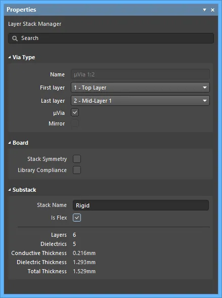
- Via Type
- Name – the name of the via. The software automatically detects the type based on the layers that have been chosen and names the via accordingly.
- First layer – the first layer the via spans.
- Last layer – the last layer the via spans.
- µVia – enable if a microvia is required.
- Mirror – when enabled, a mirror of the current via that spans the symmetrical layers in the layer stack is created. This option is available only if the Stack Symmetry option is enabled.
- Board
- Stack Symmetry – enable to add layers in matching pairs, centered around the mid-dielectric layer. When enabled, the layer stack is immediately checked for symmetry around the central dielectric layer. If any pair of layers that are equidistant from the central dielectric reference layer are not identical, the Stack is not symmetric dialog opens.
- Library Compliance – when enabled, for each layer that has been selected from the Material Library, the current layer properties are checked against the values of that material definition in the library.
- Substack – this information is for the currently selected substack (layers, dielectric, thicknesses, etc.,). As you switch from one substack to another, this information will update accordingly (for the currently selected substack).
- Stack Name – enter a meaningful substack name. This field is useful when the X/Y stackup region is being assigned a layer substack.
- Is Flex – enable if the substack is flex.
- Layers – the total number of layers in the substack.
- Dielectrics – the total number of dielectrics in the substack.
- Conductive Thickness – the thickness of conductive layer(s) in the substack. Copper signal layers are referred to as conductive layers.
- Dielectric Thickness – the thickness of dielectric layer(s) in the substack.
- Total Thickness – the total thickness of the substack.
µVias (MicroVias)
µVias are used as the interconnects between layers in high density interconnect (HDI) designs, to accommodate the high input/output (I/O) density of advanced component packages and board designs. Sequential build-up (SBU) technology is used to fabricate HDI boards. The HDI layers are usually built up onto a traditionally manufactured double-sided core board or a multilayer PCB. As each HDI layer is built on to each side of the traditional PCB, µVias can be formed using: laser drilling, via formation, via metalization, and via filling. Because the hole is laser drilled, it has a cone shape.
If a connection required a path through multiple layers, the original approach was to stagger a series of µVias using a step-like pattern. Improvements in technology and processes now allow µVias to be stacked directly on top of each other.
Buried µVias are required to be filled, while blind µVias on the external layers do not require filling. Stacked µVias are usually filled with electroplated copper to make electrical interconnections between the multiple HDI layers and provide structural support for the outer level(s) of the µVia.
Definition of a µVia

Support for µVias
- The software supports two types of µVias:
- A µVia that traverses from one layer to an adjacent layer.
- A Skip µVia, this type of µVia skips the adjacent layer, landing on the next copper layer after that.
- The Via Type is detected automatically based on the defined layer span, as shown in the image below.
- The order that the First layer and Last layer are chosen defines the drill direction for a µVia, as indicated by the direction of the conical µVia shape in the image.
- µVias are automatically stacked when traversing multiple layers during interactive routing (using available Via Types).

µVia Output Considerations
The PCB drill table and drill-type output files support µVias.
Drill Table
The PCB Drill Table includes µVia drill pairs.
 The drill table identifies each hole by size, if the same size is used on multiple drill pair layers it is flagged as mixed.
Drill Fabrication Files
NC Drill - a separate file is created for each µVia drill pair.
Gerber X2 - specific setup entries for each µVia plot.
ODB++ - a separate drill fabrication file created for each µVia drill pair.
Back Drilling of Thru-hole Vias
Main page: Controlled Depth Drilling, or Back Drilling
Back drilling, which is also known as Controlled Depth Drilling (CDD), is a technique used to remove the unused portion, or stub, of copper barrel from a thru-hole in a printed circuit board. When a high-speed signal travels between PCB layers through a copper barrel, it can be distorted. If the signal layer usage results in a stub being present, and the stub is long, then that distortion can become significant.
These stubs can be removed by re-drilling those holes after the fabrication is complete, with a slightly larger drill. The holes are back drilled to a controlled depth, close to, but not touching, the last layer used by the via. Allowing for fabrication and material variations, a good fabricator can back drill holes to leave a 7 mil stub, and ideally, the remaining stub will be less than 10 mil.


By re-drilling the hole with an oversized drill bit to a specific depth the unused portion of the via barrel is removed, improving the integrity of this signal path.
Back Drilling is enabled in the Layer Stack Manager's Tools menu and then configured in the Back Drills tab of the Layer Stack Manager.
