Welcome to the world of electronic product development in Altium's world-class electronic design software. This tutorial will help you get started by taking you through the entire process of designing a simple PCB – from idea to output files.
To learn more about a command, dialog, object, or panel, press F1 when the cursor is over that item.
The Design
The design for which you will be creating the schematic and designing a printed circuit board (PCB) is a simple astable multivibrator. The circuit is shown below; it uses two general-purpose NPN transistors configured as a self-running astable multivibrator.

Circuit for the multivibrator.

The animation of the designed PCB
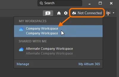
Altium NEXUS can connect to a Workspace to provide a single, secure data source and storage while affording unparalleled collaboration. It could be an Altium 365 Workspace – a Workspace hosted on the Altium 365 cloud-based infrastructure platform, or NEXUS Server Workspace – a Workspace provided through Altium NEXUS Server, a solution installed and managed by your own IT department.
This tutorial focuses on using Altium NEXUS with a connected Workspace – the most streamlined and empowered environment for your design needs. However, if you are not able to enjoy the benefits that a connected Workspace brings, you can store your design data, including projects, component libraries, and design outputs, locally on your hard drive or in a shared network resource.
To complete this tutorial, you will need to be connected to a Workspace. It is assumed that your Workspace has been activated/installed with the sample data.
► Learn more about Designing with a Connected Workspace
► Learn more about Accessing Your Workspace
You're ready to begin capturing (drawing) the schematic. The first step is to create a PCB project.
