Parent page: Working with File-based Component Libraries
The real-world component that gets mounted on the board is represented as a schematic symbol during design capture, and as a PCB footprint for board design. Altium NEXUS components can be:
-
Created in and placed from local libraries or
-
Placed directly from a connected Workspace, accessible for the entire design team.
This document outlines the creation and management of schematic libraries (
*.SchLib). To learn more about creating a component symbol itself, refer to the
Creating a Schematic Symbol page.
Symbols can be copied from the schematic editor into a schematic library, copied between schematic libraries, or created from scratch using the Schematic Symbol Generation Tool or drawing tools.
Creating a New Schematic Library
To create a new schematic library, select the File » New » Library command from the main menus and select the Schematic Library option from the File region of the New Library dialog.

After clicking Create, a new schematic library document named Schlib1.SchLib is created and shown in the Projects panel, and an empty component sheet called Component_1 displays.
The content of the library is shown in the SCH Library panel.
You are now ready to add, remove, or edit the schematic components in the new schematic library using the schematic symbol editor commands.
You also can create a schematic library of all the components that have been placed in the schematic documents of the active project by clicking Design » Make Schematic Library.
Creating a New Schematic Component
Any number of component symbols can be created in a schematic library. To create a new schematic component in an existing library, you would normally select Tools » New Component.
Since a new library always contains one empty component, you can also rename Component_1 to get started on creating a component. To do this, select Component_1 from the Design Item ID list in the SCH Library panel then click the Edit button in the panel or double-click Component_1 to open the Properties panel in Component mode. Type the new component name that uniquely identifies it in the Design Item ID field then press Enter.
Adding Models to the Schematic Component
You can add any number of PCB footprint models to a schematic component, as well as model files that are used for circuit simulation and signal integrity analysis. If a component has multiple models (for example, multiple footprints), you can select the appropriate model in the Properties panel when you place the component on a schematic. In terms of sourcing the models, you can create your own or download a vendor's model file from the web. PCB libraries can include any number of PCB footprints.
Wherever possible, Spice models used for circuit simulation (.ckt and .mdl files) are included in the supplied integrated libraries in the Library folder of your Altium NEXUS installation. If you are creating a new component, you would typically source the Spice model from the device vendor's website. You can also use the XSpice Model Wizard (Tools » XSpice Model Wizard) to create certain Spice model types to add to the component.
The schematic symbol editor's Model Manager dialog (Tools » Model Manager) enables you to view and organize your component models. For example, you can add the same model to multiple, selected components. Alternatively, you can add models to the current component from the Model region of the design space (click the upside-down arrows/caret symbol on the bottom-right of the design space as shown in the following image).

Click the highlighted caret symbol to access the Model region of the design space.
You can also add models to the current component by using the Add drop-down in the Parameters region of the Properties panel in Component mode then selecting the model.
At the schematic stage, the design is a collection of components that have been connected logically. To test or implement the design, for example, circuit simulation, PCB layout, signal integrity analysis, etc., it needs to be transferred to another design domain. To achieve this, there must be a suitable model of each component for the target domain.
-
Footprints are linked to the schematic component by adding them in the Parameters region of the Properties panel. Click the Add drop-down then select Footprint to open the PCB Model dialog to configure the footprint.

Click the Browse button to open the Browse Libraries dialog to browse available footprint libraries. If the desired footprint is not available in any of the current libraries, you will need to search for it using the Find button to open the File-based Libraries Search dialog.
-
Models are linked to the schematic component by adding them in the Parameters region of the Properties panel. Click the Add drop-down then select Simulation or Ibis Model to open the respective dialog.
As part of the process of linking the model, information about the component must be mapped from the schematic to the target model.
The 3D model is not linked directly to the component symbol. Instead, the 3D model is placed in the PCB footprint. Why? Because the 3D model must be rotated, aligned and positioned correctly, relative to the footprint, therefore, it makes sense to do this in the footprint editor. To learn more about working with 3D models and placing them in a footprint, refer to Creating the PCB Footprint.
Mapping the Model to the Symbol
The domain-specific information resides in model files that have a predefined format, such as IBIS, MDL and CKT files. There is other information needed for the system to access that domain-specific information, such as the pin-mapping and net listing between the schematic symbol and the domain-specific model. This information is defined in a domain-specific model editor, which opens when a model is added or edited. As well as referencing the model file, it will also include any pin mapping or netlisting information required for that model kind.
These are a number of predefined analog device models that are built into SPICE. For these component types, there is no separate model file required. All the information needed to model them is configured in the SIM Model editor.
To configure pin mapping for a linked footprint, open the PCB Model dialog (select the footprint in the Parameters region of the Properties panel then click  or double-click the model in the Model region) then click Pin Map to open the Model Map dialog and make any necessary edits for the Pin-Pad pairs.

Where the Footprints are Found
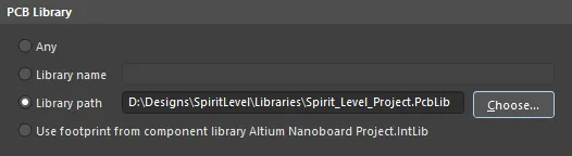
At the top of the PCB Model dialog, there is a Name field that must contain the name of the footprint. You can enter the name directly or use the Browse button to find it. At the bottom of the dialog, there is a text string that shows where that model was found.

When the named model is found, the model appears and information is displayed about where it has been found.
The software's ability to find the model is influenced by the setting that defines where it can look for models. This is the setting just below the model name. The options range from Any, meaning search all available libraries for this model, to Integrated Library or Server, which indicates that the model can only be used from the specified integrated library or Workspace.
The PCB Model dialog include these options:
| Library Option |
Behavior |
Dialog Setting |
| Any |
Searches all available libraries for a matching model. |
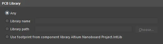 |
| Library name |
Only searches available libraries of this name for a matching model. |
 |
| Library path |
Only searches a library of this name, in this location, for a matching model. |
 |
| Integrated library |
Only searches for the model in the integrated library that the component was placed from. The integrated library must be available. |
 |
| Server |
Only searches for the model in the Workspace from which this component was placed. The software must be connected to that Workspace. |
 |
Search Locations for Model Files
When you add a model to a component in the schematic symbol editor, the model is linked; the model data is not copied or stored in the schematic component. This means the linked models must be available both during library creation and when the component is placed on a schematic sheet. When you are working in the library editor, the link from the component to the model information is resolved using the following valid search locations:
-
Libraries that are included in the current library package project are searched first.
-
PCB libraries (not integrated libraries) that are available in the currently Installed Libraries list are searched next. Note: The list of libraries can be ordered.
-
Finally, any model libraries that are located on the project search paths are searched. Search paths are defined on the Search Paths tab of the Project Options dialog (Project » Project Options). Note: Libraries that are on the search path cannot be browsed to locate a model, however, the compiler does include them when searching for a model.
Refer to the Managing Available Database and File-based Libraries section of the Searching for Components in File-based & Database Libraries page for more information about the way models are searched for in the schematic symbol editor and the schematic editor.
Using Parameters to Add Detail to the Component
Component parameters are a means of defining additional information about the component. Parameters allow you to define additional textual information about the component. This can include electrical specifications (i.e. wattage or tolerance), purchasing or stock details, designer notes, references to component datasheets - basically any purpose you choose: data your company needs in the BOM, manufacturer's data, a reference to the component datasheet, or design instruction information, such as design rules or assignment to a PCB class, etc.
Parameters can be defined in the schematic library editor during component creation using the Properties panel.
Adding Parameters to a Component
For an individual component, parameters are added in the Parameters region of the Properties panel in Component mode. As mentioned, this can be done in the library or once the component has been placed on the schematic sheet.
Use the following steps to add a parameter to a schematic component:
-
Double-click on the component name in the SCH Library panel to open the Properties panel in Component mode.
-
In the Parameters region, select Parameter from the Add drop-down.
-
Enter the desired name of the parameter and a value.
-
Ensure the Parameter's visibility option is set to enabled (
 ) if you want the name and value to display when the component is placed on a schematic sheet.
-
Click the Font Link and Other at the bottom of the Parameters region to access additional options to configure parameters.

You also can select the parameter in the design space to open the
Properties panel in
Parameter mode to configure the parameter.
Adding Parameters to Multiple Components
Parameters are a key element of each component, and it is common for many of the parameters to be used across multiple components. As well as adding them individually to each component, you can also use the Parameter Manager command (Tools » Parameter Manager) to add them to multiple components. As well as adding and removing parameters, the values of parameters can also be edited across multiple components.

The Parameter Table Editor dialog can be used to edit all of the parameters across all of the components.
Notes about editing multiple parameters:
-
Parameters can be edited across the components in a library or across components used in a schematic design using the same process. Select Tools » Parameter Manager in either the schematic or schematic library editor to start the process.
-
Because parameters can be added to a variety of different objects, the first step is to select in which object types the parameters are to be edited in the Parameter Editor Options dialog.
-
Parameter editing is performed in the Parameter Table Editor dialog. The dialog can be accessed in different ways, so the dialog caption can change. The way you work in the dialog is the same regardless of how it was accessed: use the standard Windows selection keystrokes to select the cells of interest then right-click and choose an edit action.
-
Changes are not performed immediately; they are done via an Engineering Change Order (ECO).
-
Each cell that is being changed is marked by a small colored icon. Refer to the Parameter Table Editor dialog page for a description of each icon.
Mapping a Parameter into the Component's Comment Field
The default component parameters that are displayed on the schematic are the Designator and Comment. When the design is transferred from the schematic editor to the PCB editor, the Designator and Comment strings are also the default strings that can easily be displayed on the board.
To allow you to display the value of any component parameter on the schematic and PCB, for example, to display the value of a parameter called Capacitance, you can map any component parameter into the component's Comment field using a technique known as string indirection.
This is done by entering the parameter name in the form =ParameterName. For example, to map the value of the component parameter Capacitance into the component's Comment field, enter the string =Capacitance into the Comment field of the Properties panel, as shown below. A string defined using the syntax '=ParameterName' is referred to as a special string.
Special strings are automatically converted for on-screen display. If a parameter that is mapped as a special string does not have a value, the parameter name is displayed in a gray color instead if the Display Names of Special Strings that have No Value Defined option is enabled on the Schematic - Graphical Editing page of the Preferences dialog. If this option is disabled, nothing is displayed.

Use the special strings feature to map any parameter value to the component's Comment.
Special strings allow the mapping of any parameter to any string. The string can be a component string, a free string placed on the schematic sheet, or a string placed in a schematic template. The parameter can be a component parameter, a document parameter or a project parameter. Refer to the Special Strings to learn more.
Defining Clickable Links to Reference Information
The Parameters region of the Properties panel in Component mode allows you to add a link by clicking the Add drop-down then selecting Link. This feature can be used to include links to a datasheet or a manufacturer website, for example. Any number of links can be defined for a component.

Links displayed in the panel are live, so when you click on the link text, the URL will load into your preferred browser. To edit an existing link, click anywhere in the cell away from the link text then click the edit button.
Links can be accessed via the context menu when you right-click on the placed schematic component.

Right-click on a component on the sheet to access the component links.
Links can also be included in a PDF generated from the schematic, either via the Smart PDF feature or a PDF generated from an OutputJob file. The image below shows how the list of component parameters display in the PDF. Any that are URLs can be clicked on to browse from the PDF to that location. Component parameters and links can also be included in a generated PDF by enabling the Include Component Parameters option in the Smart PDF Wizard or OutputJob options generation settings.
PDFs can be generated directly from the schematic via the Smart PDF Wizard or from an OutputJob. Click on a component in the PDF to display the parameters, as shown below.

Click on a component in the PDF to display the parameters; click on a link-type parameter to open the target.
Checking the Component and Generating Reports
To check that the new components have been created correctly, there are three reports that can be generated. Ensure the library file is saved before the reports are generated.
Component Rule Checker
The Component Rule Checker tests for errors such as duplicates and missing pins.
-
Select Reports » Component Rule Check (shortcut R, R) to open the Library Component Rule Check dialog.

-
Set the attributes you want to check then click OK. A report titled <
libraryname.ERR> displays in the design space that lists any components that violate the rule check.

-
Make any adjustments necessary to the library then rerun the report.
-
Save the schematic library. Close the report to return to the schematic editor design space.
Linkage from the component pins to the model is not checked by the Component Rule Checker. This level of linkage is checked, however, when a library package is compiled into an integrated library. Even if you do not intend to use the compiled integrated libraries, it is beneficial to create and manage your libraries using library packages.
Component Report
The Component Report lists all the information available for the active component.
-
Select Reports » Component (shortcut R, C).
-
A report titled <libraryname.cmp> displays in the design space and includes the number of parts with the pin details for each part in the component.

-
Close the report to return to the schematic editor design space.
Library Report
To create an extensive report of each component in the library:
-
Select Reports » Library Report to open the Library Report Settings dialog.

-
Configure the report settings then click OK. The report will open in Microsoft Word or your web browser depending on the style chosen.
Copying Components from Other Libraries
You also can copy components to your schematic library from other open schematic libraries and then edit their properties as required. If the component is part of an integrated library, you will have to open the .IntLib file and choose Yes to extract the source libraries. Then open the generated source library (*.SchLib) from the Projects panel.
-
Select the component that you want to copy in the Design Item ID list of the SCH Library panel so it displays in the design window.

-
Select Tools » Copy Component to open the Destination Library dialog, which lists all currently open schematic library documents.

-
Select the document to which you want to copy the component then click OK. A copy of the component will be placed in the destination library where you can edit it, if necessary.
Copying Multiple Components
You also can use the SCH Library panel to copy multiple components. Select the components in the panel using the standard Ctrl+Click or Shift+Click features, then right-click on one of the selected components and choose Copy from the pop-up menu. You can then right-click in the list and:
-
Paste the component(s) back into the same library.
-
Paste the component(s) into another open library.
-
Copy and paste components from a schematic into an open library using the same technique.
Moving a Design from One Location to Another
When a component is placed from a library into a design, it is cached in the design file so that the document can still be opened at any location without requiring its source libraries to be present or loaded. This is helpful when moving a design from one location to another since it is not necessary to move the libraries as well. Note that the original source library name and the model names are also stored within the placed component's properties.
SCH Library Panel
The SCH Library panel enables you to view and make changes to the components stored in the active schematic library document. The panel also offers the ability to pass on any changes made to components in the library directly to the schematic design document, and also to define model linking for a component.

Interactively browse, view and edit schematic library components and their pins.
SCH Library Panel Content and Use
Library Browsing
As you click on a component entry in the list, it will become the active part in the design editor window. The design editor window is editable, allowing you to change the symbol for the component and add, edit, or remove linked models for the component as required. Selecting a Pin object in the panel causes the corresponding graphical object to be highlighted (and zoomed) in the editor workspace. In this way, the SCH Library panel offers a fast and easy way to browse, view and access schematic library components and pins.
Filtering Content
The contents of the Components list can be filtered, enabling you to quickly find a particular component within the library. This is especially useful if the library contains a large number of items. Filtering can be applied using one of the methods described in the following sections.
Indirect Filtering
This filtering method uses the search field at the top of the panel to filter the contents of the list. The name masking is applied based on the entry in the field. Only those components in the list targeted by the scope of the entry will remain displayed.

To list all library component footprints again, clear (delete) the entry in the search field.
The filtering feature is not case sensitive and supports 'type-ahead' functionality, meaning that the content of the Components list is filtered as you type.
Use the * wild card operator for more elaborate filtering. For example, typing MN* will display only component footprints whose names begin with MN, or, as in the image below, typing *r34 will display only component footprints where the body of the name contains R34.

Direct Filtering
This method is available for all regions in the panel and allows you to quickly jump to an entry by directly typing within the area of the list. Masking is not applied, leaving the full content of the list visible at all times.
To use the feature for quickly finding a component footprint, click inside the Components section of the panel then type the first letter of the component footprint to which you want to jump. For example, if you wanted to quickly jump to component entries starting with the letter R, you would press R on the keyboard. The first component in the list starting with R would be made active.
If there are multiple Design Item IDs starting with the same letter and especially if the library is particularly large, type additional letters to target the specific entry you require. For example, type res to highlight the first of the RES series in the list.

To clear the current filtering to allow you to enter a different starting letter, press Esc. Use the Backspace key to clear the previously entered filter characters in sequence.
Combination Filtering
In some situations, it may be helpful to use indirect and direct filtering simultaneously. If, for example, you know that the component you want to locate has a sub-type variant of BRMZ and a prefix of AD74, this information can be used as Indirect (Mask) and Direct entries, respectively.
Panel Sections
Components
As you click on a entry in the Components list, it will become the active part in the design editor window and for the four buttons located directly beneath the list. These buttons provide the following commands that can be used with respect to the list of components:
-
Place - click to place the active component onto a schematic design document. When clicked, the schematic document that is used will depend on whether or not any schematic documents are currently open.
-
If there are no schematic documents open, clicking the button will cause a new schematic document to be created that will be the active document in the design editor window. The active library component will appear floating on the cursor, ready for placement.
-
If one or more schematic documents are currently open, the last document to have been active (regardless of the project to which it belongs) will be made the active document in the design editor window and the active library component will appear floating on the cursor, ready for placement.
-
Add - click to add a new component to the library document. The New Component dialog will open. Enter the required name for the new component to be added to the list. A blank sheet will be opened in the design editor window ready for you to define the component.
-
Delete - click to permanently delete the selected component(s) from the library document. A confirmation dialog will open asking whether or not to proceed with the deletion.
-
Edit - click to open the Properties panel in which you can view/edit properties associated with the active component. The panel provides access to create links to new models or edit existing ones. Double-clicking on a Design Item ID entry will also open the Properties panel.

Right-Click Menus
Right-clicking on an entry in the Components list will open a menu of commands.

The commands are as follows:
-
Select all - quickly select all component entries in the list.
-
Update Schematic Sheets - click to pass on all changes made to components within the active library document to all open schematic design documents. All instances of changed components that exist on the design documents will be updated.
-
Model Manager - access the Model Manager dialog in which you can add, edit or remove models with respect to any of the components contained in the active library.

-
Copy - place a copy of the selected component(s) onto the schematic library editor's internal clipboard.
-
Cut - place a copy of the selected component(s) onto the schematic library editor's internal clipboard and permanently delete the component(s) from the library. A dialog will appear asking for confirmation to proceed with the deletion.
-
Paste - paste a component from the schematic library editor's internal clipboard into the active library document.
-
Delete - use to permanently delete the selected component(s) from the library document. A dialog will appear asking for confirmation of whether or not to proceed with the deletion.
Notes
-
Standard Ctrl+Click and Shift+Click functionality is supported for selection of multiple entries in a list.
-
The active component is the one that has its symbol and corresponding model information currently displayed in the design editor window. A component can be active without necessarily being selected in the Components list.
-
Ctrl+Click over a selected entry in a list to deselect it.
-
The keyboard shortcuts Up Arrow, Home, End, and Down Arrow can be used to display the previous, first, last, and next entry in a list region, respectively.
-
Multi-part components appear in the list with
 (expand) next to them. Each part is listed as a sub-entry below.
-
In sections of the panel where multiple columns of data exist, the data may be sorted by any column by clicking on the header for that column. Click once to sort in ascending order; click again to sort in descending order.
-
You can change the order in which columns of data are displayed. To move a column, click on its header and drag it horizontally to the required position. A valid position is indicated by the appearance of two positional arrows.
-
The component that you paste into the active library document can originate from either a schematic design document or another schematic library document.
-
If multiple components have been copied to the clipboard from the main design in the schematic editor, all components in the selection will be pasted into the library document.
-
If the same component is pasted into the library more than once, or if more than one new component is added to the library without renaming, the copies are distinguished by the suffix _1, _2, _3, etc.
-
A schematic design document must be open in order to pass on changes made to components in the library document.
-
When a new schematic library document is created the panel will contain a single, blank component - Component_1.
