Parent page: Capturing Your Design Idea as a Schematic
It is not unusual for an electronic design to included repeated sections of circuitry. It might be a stereo amplifier, or it might be a 64 channel mixing desk. This type of design is fully supported, by a feature-set known as multi-channel design.

The two decoder channels of a video multiplexer, using a multi-channel design structure means the decoder channel is only captured once.
In a multi-channel design, you capture the repeated circuit once, then instruct the software to repeat it the required number of times. When the design is automatically compiled, it is expanded out in memory, with all components and connectivity repeated the required number of times, in accordance with a user-defined channel naming scheme.
The logical design that you capture is never actually flattened, the source always remains as a multi-channel schematic. When you transfer it to the PCB layout, the physical components and nets are automatically stepped out the required number of times. You have full access to the standard cross-probing and cross-selecting tools available for working between the schematic and the PCB. There is also a tool in the PCB editor to replicate the placement and routing of one channel across all other channels, with the ability to easily move and re-orient an entire channel.
Dynamic Compilation
Related article: Compiling and Verifying the Design
The design connectivity model is incrementally updated after each user operation through dynamic compilation. You do not need to manually compile the project, as this is done automatically. For a design project, the automatic compilation process performs three functions:
- Instantiates the design hierarchy.
- Establishes net connectivity between all the design sheets.
- Builds an internal Unified Data Model (UDM) of the design.
This ensures that any design changes that are made are immediately reflected in the Navigator and Projects panel.
The compiled model of the project is referred to as the Unified Data Model (UDM). The UDM includes detailed descriptions of every component in the design, and how they are connected to each other.
The
Schematic.DynamicCompiler option in the
Advanced Settings dialog must be enabled in order for dynamic compilation to occur. The option is enabled by default.
In order to check for logical, electrical, and drafting errors between the UDM and compiler settings, you must validate the project. This command is accessed by choosing the Project » Validate Project command from the main menus or by right-clicking over the entry for a project in the Projects panel, and choosing the Validate Project command from the context menu.
Any violations that are detected by the Compiler will be listed as warnings and/or errors in the Messages panel panel. The Compiler uses the options defined on the Error Reporting and Connection Matrix tabs of the Options for Project dialog (as applicable to the project type), when checking the source documents for violations.
In versions of the software prior to Altium NEXUS 20.0, the project had to be manually compiled to build the Unified Data Model. Since then, the design data model is incrementally updated after each user operation through dynamic compilation - creating what is referred to as the Dynamic Data Model (DDM). There is no manual compilation of the project involved, it is all done automatically. The design connectivity model is incrementally updated after each user operation, courtesy of dynamic compilation.
The Unified Data Model
To understand multi-channel design, it helps to understand how the design data is managed. A fundamental element of the software is the Unified Data Model (UDM). When the project is automatically compiled, a single, cohesive model is created, which sits central to the design process. Data within the model can then be accessed and manipulated using the various editors and services within the software. Rather than using a separate data store for each of the various design domains, the UDM is structured to accommodate all information from all aspects of the design, including the components and their connectivity.

The Unified Data Model makes all of the design data available to all of the editors and helps deliver sophisticated features like multi-channel design.
The UDM, in combination with the hierarchical design system, is leveraged to deliver the multi-channel design capabilities. The "channel" is the circuitry within a Sheet Symbol - below this Sheet Symbol can be a single sheet, or it can be an entire branch of the project structure, containing other sub-sheets. You can also create channels within channels, in a 2-level multi-channel design the upper channels are referred to as banks, with the lower level ones referred to as channels.
Because this full, PCB-ready description exists in memory it is then possible to repeat a section of circuitry, as long as there is a systematic way to handle repeated objects, such as component designators and nets. The systematic naming is defined in the Multi-Channel tab of the Options for Project dialog, as discussed below.
Creating a Multi-Channel Design
A design is multi-channel when a section of the circuitry is repeated. This is done at the sheet symbol level, either by:
- placing multiple Sheet Symbols that all reference the same child schematic, or
- configuring a single Sheet Symbol to repeat the referenced child schematic the required number of times
. Second image - the InputChannel.SchDoc is repeated eight times and the OutputChannel.SchDoc twice by using the Repeat keyword.")

First image - there are four Sheet Symbols, all referencing the same child sheet (PortIO.SchDoc). Second image - the InputChannel.SchDoc is repeated eight times and the OutputChannel.SchDoc twice by using the Repeat keyword.
These two approaches to creating a multi-channel design are shown in the images above. In the first image, there are four sheet symbols that all reference the same child sheet (PortIO.SchDoc). In the second image, the InputChannel.SchDoc is repeated eight times and the OutputChannel.SchDoc is repeated twice, by the presence of the Repeat keyword in the Designator field of the Sheet Symbol.
Repeated component designators and net names in the project are resolved by applying a standard naming scheme. For example, one naming scheme is to add a channel index to the repeated components and net identifiers (Net Labels and Ports), as shown in the highlights in the images below.
Note the tabs that appear across the bottom of the schematic when the project is opened. The Editor tab contains the logical design as you have captured it, the other compiled tabs (COUT1 and COUT2) also appear, they represent the physical design that will be transferred to the PCB editor. There will be a tab for each physical channel.


The compiled project, showing the tab for the logical view, and a tab for each physical channel that is transferred to the PCB. Note how the repeated designators and net identifiers are managed.
The channel naming scheme is defined on the Multi-Channel tab of the Options for Project dialog.
The Repeat Keyword
As mentioned, a channel is repeated by placing multiple sheet symbols that reference the same child sheet, or by including the Repeat keyword in the Sheet Symbol's Designator field. When the Repeat keyword is used, the Sheet Symbol is drawn as a set of stacked Sheet Symbols.

The Repeat statement defines the channel designator and the number of channels. Note how the Sheet Symbol is drawn as a set of stacked symbols, to signify repeated channels.
Each channel is identified by a channel designator, which comes from the Sheet Symbol Designator. When the design is channelized by placing multiple Sheet Symbols, the channel designator is the Designator value defined for each Sheet Symbol. If the design is channelized by the use of the Repeat keyword, the channel designator is the ChannelIdentifier+ChannelIndex defined by the Repeat keyword.
The syntax of the Designator field when the Repeat keyword is used is as follows:
Repeat(<ChannelIdentifier>,<ChannelIndex_1>,<LastChannelIndex_n>)
When the
New Indexing of Sheet Symbols option is enabled on the
Options tab of the Project Options dialog, any digit or number may be used as the first or last index of a repeated Sheet Symbol, including 0; the last index must always be larger than the first index and negative numbers are not allowed.
Multi-Channel Naming
The concept of being able to capture once and then repeat - multi-channel design - is delivered by building on the software's unified data model (UDM). Repeated components are named using a systematic naming scheme, which is configured on the Multi-Channel tab of the Options for Project dialog, as shown below.
The dialog includes an upper section used to control the naming of the Rooms, and a lower section used to control the naming of the components within those Rooms. At the Room level, there are 2 flat naming styles and 3 hierarchical naming styles, typically you would only need to choose a hierarchical naming style if the design has channels within channels. Otherwise, a flat Room naming style is shorter and easier to understand.
For the component naming, the $Component$ChannelAlpha or the $Component_$ChannelIndex option will give the shortest, and most easily interpreted component designation. It is also possible to construct your own designator naming scheme, using the available keywords.
 are managed by applying a systematic naming scheme, chosen on the Multi-Channel tab of the Project Options dialog.")
Repeated components (and nets) are managed by applying a systematic naming scheme, chosen on the Multi-Channel tab of the Project Options dialog.
- As well as the components, the Component Naming scheme is used to uniquely identify nets within each channel. This scheme is used to rename net identifiers, including Net Labels and Ports.
- The display of these names on the schematic sheet is discussed below in the Displaying the Compiled Names section.
The Role of the Room
A Room is a PCB design object used to define an area on the board, which can then be used in two ways:
- Contain objects - while a room is placed like any polygonal shape object, it is actually created as a Placement design rule. Part of a Room's definition is to specify the objects that must be contained within that room - which is often components. When that room is moved, all the components within the room move too.
- To scope other design rules - as well as being a rule in their own right, rooms can also be used to scope other design rules. For example, one routing width design rule defines the routing width for a class of nets, then a higher-priority design rule, with a scope of Room, can specify a different width to be applied to that class of nets, within that Room.
Rooms work very well with a multi-channel design. They can be created automatically as the design is transferred from the schematic editor to the PCB editor, based on options on the Class Generation tab of the Project Options dialog, with a room for each Sheet Symbol. As well as clustering the components in that channel, the room can then be used in the naming of the components within that room. Rooms and their role in the board design process are discussed further in the Multi-Channel PCB Design section of this article.
If you prefer a flat component numbering system, it is possible to replace the systematic naming scheme by performing a Board Level Annotation. It is called Board Level Annotation because the component designators are only applied to the full, compiled design (physical design) that is destined to become the PCB.
Connectivity in a Multi-Channel Design
For a multi-channel design, set the Net Identifier Scope to Automatic, Hierarchical or Strict Hierarchical. A multi-channel design must be hierarchical because the software uses this structural model to instantiate the channels in memory when the design is compiled.
There are two different connectivity requirements that the software must support for a net connecting to a repeated channel, the net will either be:
- common to all channels, or
- unique in each channel.
The level of support for this depends on which method has been used to define the channels (multiple Sheet Symbols, or via the Repeat keyword). If a design uses multiple Sheet Symbols (an individual Sheet Symbol for each channel), then the net connectivity is explicit, as defined by the wiring placed by the designer.

This design uses the Repeat keyword to create multiple channels.
If the design uses the Repeat keyword, then the following connectivity conventions apply.
| Passing a Net to all Channels |
If a net needs to be available in all channels it is simply wired to a Sheet Entry, as shown for the Monitor net connected to the InputChannel.SchDoc Sheet Symbol in the image above. The nets Effects, MB1 and MB2 will also be available on all of the channels. Nets in a bus are handled the same way, when a bus is connected to a Sheet Entry then each element in that bus is available on all of the channels. |
| Passing a net to a Specific Channel |
To allocate a single net from a bus to each channel, the Repeat keyword is used in the Sheet Entry, as is shown for the Headphone bus in the image above, where the Sheet Entry has the name Repeat(Headphone). In this case, the net Headphone1 will connect to the channel CIN1, Headphone2 will connect to channel CIN2, and so on. It is not possible to pass an individual net to just one channel if the Repeat keyword has been used to create the channels. If this is required, you must place an individual Sheet Symbol for each channel. |
How the Nets are Named
Ultimately, each net can only have one name on the PCB (one PCB net cannot have two names). The software automatically resolves nets with multiple names to have just a single name in a project- it is important that you configure the naming options in a multi-channel design to ensure that your nets are labeled in a way that is meaningful to you. The net naming options are in the Netlist Options section of the Options tab of the Options for Project dialog.

A good approach to set these options in a multi-channel design is to enable the Higher Level Names Take Priority option and to also place Net Labels on all nets that connect to a channelized child sheet.
As an example, consider the images below. Note that both of the Sheet Symbols point to the sheet PCB_Decoder.SchDoc, so there are 2 channels of this circuit, identified as U_PCB_DecoderA and U_PCB_DecoderB.
The Sheet Symbol includes a Sheet Entry called TDI, which is the Test Data In line in a JTAG boundary scanning chain. TDO (Test Data Out) from DecoderA then connects to the TDI of the next device in the chain, which is in the DecoderB channel.

The two decoder channels are created by placing two Sheet Symbols that both reference the same schematic, PCB_Decoder.SchDoc.
When the project is opened, the channel tabs U_PCB_DecoderA and U_PCB_DecoderB appear at the bottom of the schematic view, these tabs show the physical design as it will be passed to the PCB editor. In the images below, the schematic for the decoder circuit as it was captured is shown in the Editor tab on the left below, followed by the two physical channels for that schematic, U_PCB_DecoderA and U_PCB_DecoderB.
In the original captured schematic, the net was labeled TDI by the designer (first image). Note how the software has applied the higher-level net name, TDO_CONTROLLER, in the DecoderA tab (second image), as it is a higher-level net name (which has been set to have priority in this design). For DecoderB there is no higher-level name defined, so the original net name, TDI, has been identified in this channel as TDI_2 (third image) because that is the naming scheme defined on the Multi-Channel tab of the Project Options dialog (the Component Naming scheme is used to identify both components and nets within each channel).


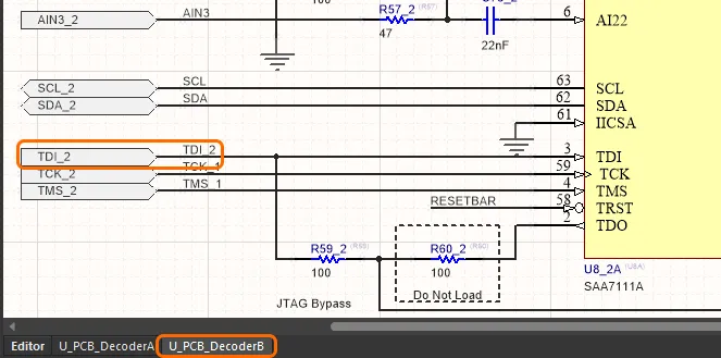
The PCB_Decoder.SchDoc schematic: first image - the captured schematic; second and third image - the compiled view of the two channels.
Displaying the Compiled Names
Tracing and analyzing the nets in a multi-channel design can be confusing, as the names have to change to identify nets that are repeated, but continue to be unique. To help with this, there are a number of options to control the display of compiled object names, including component Designators, Net Labels and Ports. There are also options for Sheet and Document Numbers, these will be important when you are ready to generate print-type output.
The display of compiled object names is configured in the Schematic - Compiler page of the Preferences dialog and is shown in the image below.

Configure the display of compiled object names, superscripts are helpful for component designators.
Typically you will want the designators and Net Labels displayed, Ports are handy if you are diagnosing an issue. Sheet Numbers and Document Numbers are also important and must be correctly configured, you'll find links to information about component and sheet numbering in the Design Annotation section.
If the Display superscript if necessary option is chosen, the current document view will include the object identifier from the non-visible view as a superscript. Configure these to suit your preferences.
 of a multi-channel design. Note how the designators and net names of the original logical schematic are displayed as superscripts.")
The view for channel 2 (CIN2) of a multi-channel design. Note how the designators and net names of the original logical schematic are displayed as superscripts.
Wondering why some of the schematic elements are dimmed in the channel (physical) tabs? The default is to show the objects that can be edited in the channel tab in the standard display strength, with non-editable objects dimmed. The dimming is set in the System - Navigation page of the Preferences dialog. The advantage of dimming objects is that it helps prevent you from trying to perform edit-actions that cannot be supported, such as moving a Net Label in a channel tab. Set the Dim level as required.

Resolving Multiple Net Name Errors
The schematic editor's error checking options default to flag every instance of a net with multiple names. This can occur when you intentionally change the name, for example when a net enters a sheet symbol and you prefer to use a different name within that sheet. The image below shows a number of examples of this, where the Left and Right outputs are bundled into a bus on the top sheet but are called Left and Right in the Sheet Entries.
A bus has been used as it allows the two output channels to be represented by a single sheet symbol with a Repeat keyword. If separate wires were used for the Left and Right channels then the designer would have needed to place separate sheet symbols for the Left and Right output channels (both pointing to the same child schematic sheet), and then wire each output to its respective output sheet symbol.
You must instruct the software on how to deal with multiple net identifiers. To do this, you will need to either:
- Set the Nets with multiple names error check to No Report in the Error Reporting tab of the Options for Project dialog. This is not the preferred option, as it blocks all checking of this error condition throughout the design. Alternatively, you can,
- Place a Specific No ERC Directive on the affected nets, by right-clicking on an Error/Warning in the Messages panel and selecting the Place Specific No ERC Marker for this violation command. Doing this will put you into the NoERC object placement mode, with a pre-configured Specific NoERC marker attached to the cursor, ready to place on the net in error. After placing, double-click to configure the style and color.

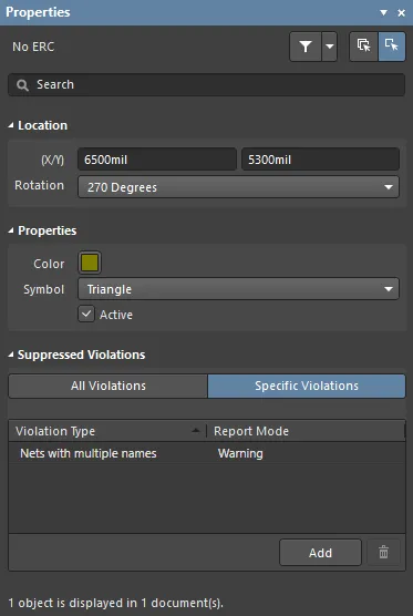
Note the small triangle circled in orange; this is a specific No ERC marker that has been placed to disable the Duplicate Net Names errors on the MB1 and MB2 nets.
Design Annotation
A key part of the design capture process is to annotate the design, that is, to give each component and each schematic sheet a unique identifier. This is a two-stage process in a multi-channel design, firstly the components you've placed and sheets you've drawn must be numbered. Then the components and sheets that are instantiated by the repeated channels must also be numbered.
► Learn more about Annotating the Components
► Learn more about Numbering the Sheets
Multi-Channel PCB Design
When you transfer a design from the schematic editor to the PCB editor, the components from each sheet are clustered in a PCB placement room if Room creation is enabled in the Project Options.
The big advantage of using rooms in a multi-channel design is that the PCB editor supports duplicating the placement and routing from one room (channel) to the other rooms (channels). Rooms can also be moved as if they are a single object, simplifying the process of arranging the channels on the PCB.

The eight input and two output channels after the design was transferred from the schematic editor to the PCB editor, the red areas are the rooms.
The Role of the PCB Room
A Room is a PCB design object used to define an area on the board, which can then be used in two ways:
- Contain objects - while a room is placed like any polygonal shape object, it is actually created as a Placement design rule. Part of a Room's definition is to specify the objects that must be contained within that room - which are often components. When that room is moved, all the components within the room move too.
- To scope other design rules - as well as being a rule in their own right, rooms can also be used to scope other design rules. For example, one routing width design rule defines the routing width for a class of nets, then a higher-priority design rule, with a scope of Room, can specify a different width to be applied to that class of nets, within that Room.
Rooms work very well in a multi-channel design. They can be created automatically as the design is transferred from the schematic editor to the PCB editor, based on options in the Class Generation tab of the Options for Project dialog, with a room for each Sheet Symbol. As well as clustering the components in that channel, the room can then be used in the naming of the components within that room.
Useful Room Manipulation Commands
- Design » Rooms - this sub-menu has a number of useful commands for defining and modifying rooms.
- Design » Rooms » Copy Room Formats - use this command to replicate the placement and routing of one room (channel), to the other rooms (channels)
- Design » Rooms » Move Room - a room can be moved by clicking and holding, anywhere where there is no other design object under the cursor. The cursor will snap to the nearest component pad, or room vertex (whichever is closer). Use this command when you cannot click and hold without clicking on a design object.
- Edit » Select » Room Connections - use this command to select all copper segments that start on a pad and end within the room.
How the Components are Linked
Each schematic component links to its PCB component through a Unique Identifier (UID). The UID is assigned when the schematic component is placed on the sheet and is then assigned to the PCB component when the design is transferred to the PCB editor. This scheme would be adequate for a simple design but is not capable of supporting a multi-channel design, where the same schematic component is repeated in each physical channel (so the PCB components would have the same UID).
To cater for this, the UID for the PCB component is created by combining the UID of the parent Sheet Symbol with the UID of the schematic component. The syntax of the PCB UID changes slightly, depending on how the multi-channel design has been created.
For a multi-channel design created by placing multiple Sheet Symbols that all reference the same schematic sheet, then each Sheet Symbol can provide a unique ID, so the PCB UID has the format:
\SheetSymbolUID\SchComponentUID
For a multi-channel design created using the Repeat keyword, there is only 1 Sheet Symbol UID available, so the PCB UID also includes the ChannelIndex, in the format:
\ChannelIndex+SheetSymbolUID\SchComponentUID
Component links are managed via the Edit Component Links dialog (Project » Component Links command in the PCB editor). When changes are applied in this dialog, the PCB UIDs are updated to match the schematic UIDs.
Displaying the designators on the PCB
It can be difficult to position the designator strings in a multi-channel design, as they can be quite long. As well as choosing a naming option that results in a short name, another option is to display just the original, logical component designation instead. For example, C30_CIN1 would display as C30. This would require some other notation being added to the board to indicate the separate channels, such as a box being drawn around each channel on the component overlay.
You can select between Logical and Physical designator display on the PCB in the Other section of the PCB editor Properties panel (View » Panels » Properties). If you choose to display the logical designators for components in a multi-channel design, these will be displayed on the PCB and in any output generated, such as prints and Gerber's. The unique physical designators, however, are always used when generating a Bill of Materials.
► Learn more about Annotating the Components
If you prefer a flat component numbering system, it is possible to replace the systematic naming scheme by performing a Board Level Annotation. It is called Board Level Annotation because the component designators are only applied to the full, compiled design (physical design) that is destined to become the PCB.
These Board Level Annotations are stored in a .Annotation file, which maps each logical designator to the assigned physical designator. This file is part of the project so you will be prompted to save it.
Parametric Multi-Channel Hierarchical Design
The challenge with reusing a section of the design, for example, linking a Sheet Symbol on your current project to your company's preferred power supply schematic, is that the values of the components are not always fixed from one design to the next.
Parametric Hierarchical Design solves this - it allows you to move the specification of the component values from the schematic sheet, into the sheet symbol that references that sheet. This capability also works perfectly with multi-channel design, allowing you to have different component values in each channel. Note that it does require that each channel has its own Sheet Symbol, as this is where the component values are stored.
For example, a graphic equalizer can have the same circuit repeated many times, with the only difference between each channel being the component values. So a capacitor might take the values 0.12µF, 0.056µF, and 0.033µF in the different channels. Implementing this is simple since you specify these values in the Sheet Symbol referencing each channel, eliminating the need to have many similar schematics with only the component values being different.
Parametric components are defined by declaring their value as a parameter of the sheet symbol above then referencing that parameter on the target component. The image below shows the top sheet for a graphic equalizer on the left, with the parameters of the 1KHz Sheet Symbol next to it. The image also shows the lower-level captured schematic and the compiled 1KHz channel (as selected by the lower tabs).

A graphic equalizer with different capacitor and resistor values in each channel; the actual component values are defined in the Sheet Symbols, so only one lower-level schematic needs to be captured.
Each of those Sheet Symbol parameters is also defined as the value of a parameter in a schematic component on a lower-level sheet, as shown in the image below. The value of each Sheet Symbol parameter is passed to the relevant schematic component, where it is then mapped into the component's Comment field. Note that if a Value parameter is directly used to show the value of a schematic component, rather than the component's Comment parameter, the only requirement is to map the Sheet Symbol parameter to the component's Value parameter (Value=C2_Value) and make it visible.

Because the Value parameter has a value of =C2_Value, the compiler knows that it must look for the actual component value in a higher-level Sheet Symbol.
Parametric hierarchy is not limited to component values. You can parametrically reference any component parameter, and also other object text labels on the schematic sheet with the exception of fundamental connectivity elements such as component IDs, Port objects and document file names. If you refer to parameters from a symbol that is many sheets up in the hierarchy, the system will search the hierarchy until it finds the matching parameter.
Download the reference design \Parametric Hierarchy\AudioEqualizer.PrjPcb for an example of how to correctly configure the Sheet Symbol and Component parameters.
If you have trouble downloading a reference design:
- Sign in to Altium Live in your browser before attempting to download.
- Use either Firefox, Chrome or Microsoft Edge to download.
