 Документация Altium Designer
...
((Design Objects Reference))_AD
PCB Design Objects in Altium Designer
Документация Altium Designer
...
((Design Objects Reference))_AD
PCB Design Objects in Altium Designer
Working with a Polygon Pour Object on a PCB in Altium Designer
Parent Page: PCB Objects
 being used to create a large GND area on a board.")
A Polygon Pour (brighter red) being used to create a large GND area on a board.
Summary
A polygon pour is a group design object that is made up of simpler primitive objects. Polygon pours are used to create a solid or hatched (lattice) area on a PCB layer, using either Region objects or a combination of Track and Arc objects. Also referred to as copper pours, polygon pours are similar to a region except that they can fill irregularly shaped areas of a board as they automatically pour around existing objects, connecting only to objects on the same net as the polygon pour.
On a signal layer, you can place a solid polygon pour to define an area for carrying large power supply currents, or as a ground-connected area for providing electro-magnetic shielding. Hatched polygon pours are commonly used for ground purposes in analog designs.
Availability
Polygon Pours can only be placed in the PCB Editor. You can place them directly or create them from selected primitives. To place a polygon, switch to the required layer then perform one of the following:
- Choose Place » Polygon Pour from the main menus.
- Click the Polygon Pour button (
 ) in the drop-down on the Active Bar located at the top of the workspace. (Click and hold an Active Bar button to access other related commands. Once a command has been used, it will become the topmost item on that section of the Active Bar).
 - Right-click in the workspace then choose the Place » Polygon Pour command from the context menu.
Placement
After launching the command, the cursor will change to a cross-hair and you will enter polygon pour placement mode.
- Position the cursor then click or press Enter to place.
- Continue placing further polygon pours or right-click or press Esc to exit placement mode.
Additional actions that can be performed during placement are:
- Press the Tab key to pause the placement and access the Polygon Pour mode of the Properties panel from where its properties can be changed on-the-fly. Click the workspace pause button overlay (
 ) to resume placement.
 - Press the Spacebar to rotate the polygon pour counterclockwise or Shift+Spacebar for clockwise rotation. Rotation is in accordance with the value for the Rotation Step defined on the PCB Editor – General page of the Preferences dialog.
Placement Modes
- While placing a polygon there are five available corner modes, four of which also have corner direction sub-modes. During placement:
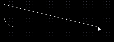
- Press Shift+Spacebar to cycle through the five available corner modes: 45 degree, 45 degree with arc, 90 degree, 90 degree with arc, and Any Angle.
- Press Spacebar to toggle between the two corner direction sub-modes.
- When in either of the arc corner modes, hold the , or . key to shrink or grow the arc. Hold the Shift key as you press to accelerate arc resizing.
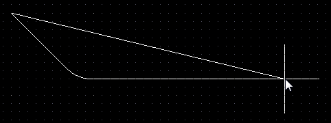
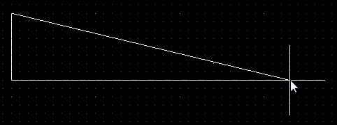
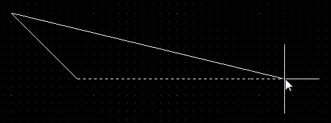
- Press the 1 shortcut key to toggle between placing two edges per click or one edge per click. In the second mode, the dashed edge is referred to as the look-ahead segment (as shown in the last image in the set below).
- Press the Backspace key to remove the last vertex.


Press Shift+Spacebar to cycle through the five available corner modes; press the 1 shortcut to toggle placement between two edges or one edge.
Defining a Polygon from Selected Objects
As well as interactively placing a polygon, they can also be created from a set of existing track and arc objects that define a closed shape. To define a polygon from an existing closed shape:
- Select all primitives that form the closed shape
- Click Tools » Convert » Create Polygon from Selected Primitives .
The polygon will be created with its Fill Mode set to Outline. Note that the original selected primitives are not removed and the new polygon is poured inside the selected objects. Double-click to repour the new polygon as solid or hatched. Note that the edge of the new polygon will lay along the centerline of the selected objects that were used to create it.
As the Create Polygon from Selected Objects algorithm uses the centerline of the selected objects, it requires that the end and start locations of touching objects are exactly co-incident (at the same location). If this is not the case, a Confirm dialog will appear, giving the location where the algorithm failed and also providing the opportunity to instruct the algorithm to attempt to define the polygon from the edges of the objects instead. As long as the selected objects overlap slightly, this option should create a polygon with the edge of the polygon tracing the outer edge of the selected objects.
Graphical Editing
The following sections describe a number of commands available to graphically modify a polygon.
Move Polygon Vertices
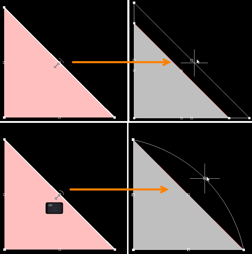
Polygons contain two points or "handles" with which to edit the shape of the polygon.
- Full Handles - these filled handles are located at the corners of the polygon.
- Empty Handles - these blank handles are located in the centers of the segments created by the Full Handles.
An existing polygon can be reshaped by moving these handles, or vertices, located at each corner or at the center of each edge.
To modify the polygon shape:
- Click and select a polygon, which will highlight the vertices for the polygon and change the cursor to a crosshair.
- Click on a Full Handle to move that corner.
- Click along an edge to move the entire edge.
- Click on an Empty Handle to move the whole side (for track and for arc).
- Ctrl+Click on an Empty Handle to break that edge into two edges. Ctrl only needs to be held at the beginning of movement. The Shift+Spacebar hotkeys can then be used to cycle through modes (arc, miter, and any angle).

The top images show empty handle editing. In the bottom images, Ctrl has been clicked while grabbing the handle to move for editing.
- If the any angle placement mode creates unwanted vertices or to remove extra vertices in general, click Ctrl and grab the central full handle. An X icon appears over the handle and dragging the edge will reduce the vertices on that edge to one.

- When you have finished, right-click then select Polygon Actions » Repour Selected to repour the polygon in its new shape.
Modify Polygon Border
In addition to vertex editing, you also can use the Polygon Actions » Modify Polygon Border right-click command to easily change the shape of polygons. Once the command is launched, the cursor becomes a crosshair. Each time you click, a new vertex is added. As during polygon placement, the Shift+Spacebar shortcuts can be used to change corner shapes.
Polygon Pour Cutout
To create a cutout or hole inside a polygon, place a polygon pour cutout on top of the existing polygon. To do this:
- Click Place » Polygon Pour Cutout.
- The cursor will change to a crosshair, starting inside the boundary of the polygon. Click the Left Mouse button to define the starting location.
- Move the cursor across the polygon. The cutout is actually a Region object with the Polygon Cutout option enabled. Press Shift+Spacebar to cycle through the region corner modes.
- Continue to click and move the mouse to define the cutout outline.
- Right-click to exit polygon cutout placement mode.
- The original polygon must now be repoured. Click on it to select it, then use the Tools » Polygon Pours » Repour Selected command from the main menus - it will pour around the new cutout.
Slice Polygon Pour
An existing polygon can be sliced into two smaller polygons. To do this:
- Click Place » Slice Polygon Pour.
- The cursor will change to a crosshair, starting outside the boundary of the polygon. Click the Left Mouse button to define the starting location.
- Move the cursor across the polygon. The slicing process uses the Line placement mode to define both the slice path and width. Press Tab to change the width; press Shift+Spacebar to cycle through the line placement corner modes.
- Continue to click and move the mouse to define the slice path.
- Once the slicing line has been placed across and out the other side of the polygon, right-click to terminate line placement.
- Right-click a second time to terminate slicing. A Confirm dialog will appear asking if you want to split the polygon into two; click Yes to split it.
- A second Confirm dialog will appear asking if you want to rebuild two polygons. Click Yes to rebuild the two new polygons.
Since these are now two independent polygons, each can be edited and repoured as required.
Combining Selected Polygon Pours
Two or more polygon pour objects can be combined by performing the following sequence of actions:
- Place new (or drag existing polygon pours) so that they are overlapping each other as required.
- Select all polygon pours that are to be combined.
- Right-click over one of the pours in the selection then choose the Polygon Actions » Combine Selected Polygons command from the context menu.
 Combining two existing polygon pours to make a single polygon pour.
Subtracting Selected Polygon Pours
One or more polygon pour objects can be subtracted from another 'base' polygon pour by performing the following sequence of actions:
- Place new or drag existing polygon pours so that they are overlapping the required base polygon pour. This is the pour to be 'subtracted from'.
- Select the base polygon pour followed by all polygon pours that are to be subtracted from it.
- Right-click over one of the pours in the selection then choose the Polygon Actions » Subtract Polygons From Selected command from the context menu.
 Subtracting two existing polygon pours from an existing 'base' polygon pour.
Non-Graphical Editing
The following methods of non-graphical editing are available:
Via the Properties Panel
Properties page: Polygon Pour Properties
The properties of a Polygon Pour can be edited in the PCB editor's Properties panel, which allows editing of all item(s) currently selected in the workspace.
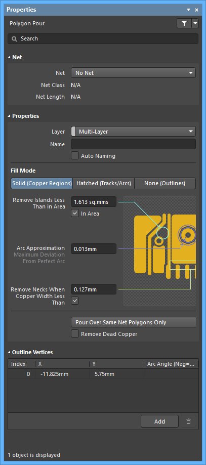
During placement, the panel can be accessed by pressing the Tab key.
To access the properties of a placed Polygon Pour:
- Double-click on the Polygon Pour.
- Right-click on the Polygon Pour then select Properties from the context menu.
- If the Properties panel is already active, click once on the Polygon Pour to select it.
Polygon Fill Modes
The polygon pour placement engine can construct polygons from either solid regions or from a combination of tracks and arcs. To help you decide which of these to use, consider the following:
- Region-based polygons result in far fewer objects being placed making for: smaller files; faster redraws, file opening, DRC and net connectivity analysis; and smaller output files since the region object is fully supported in Gerber and ODB++.
- Track/Arc-based polygons allow a hatched polygon to be created by setting the Track Width to be smaller than the Grid Size. Note that they can also be solid by setting the Track Width to be larger than the Grid Size.
- Outline Only polygons are simply Track/Arc polygons without the internal tracks and arcs.

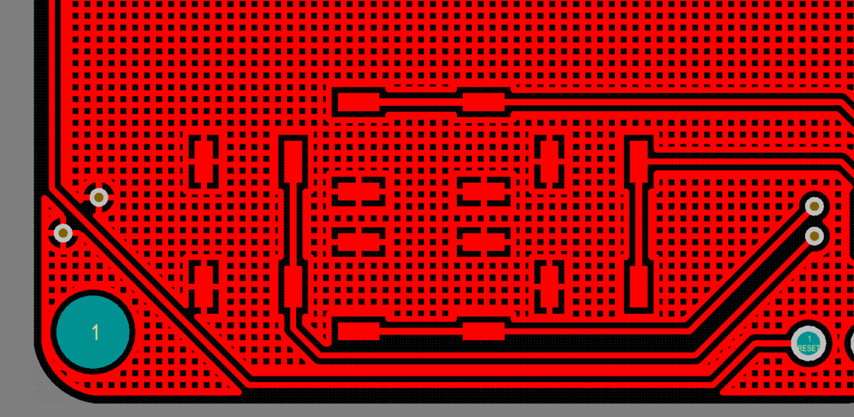 The same Polygon poured using regions then poured using tracks/arcs.
Remove Islands Less Than
Remove any areas of copper that are less than the specified area. This option is area-based only; it does not consider if that island is connected to a pad or via. Note that all small unconnected areas of copper are always removed if the Remove Dead Copper option is enabled in the Properties panel.
Arc Approximation
In a region-based polygon, circular holes are approximated by a series of straight edges. Reducing this value will result in a larger number of straight edges being used to give a better approximation of an arc.
Remove Necks When Copper Width Less Than
Use this to remove narrow slithers of copper. Note that when this option has a larger value, there will be a greater number of tight locations where the polygon cannot pour. The value should not be smaller than the narrowest track width that the fabricator can support. As a guide, it can be set to be the same as the narrowest track width used on the board.
Net Options
- The Net Options includes a drop-down with the following options:
- Don't Pour Over Same Net Objects - pour the polygon in free space only.
- Pour Over All Same Net Objects - pour the polygon in free space and also pour over any objects that belong to the same net (i.e., tracks, arcs, fills, regions, other polygons).
- Pour Over Same Net Polygons Only - pour the polygon in free space and also pour over existing polygons that belong to the same net.
- Remove Dead Copper - if this option is enabled, any area of polygon that does not include at least one connection to another net object (such as a pad or via) is automatically removed. Note that if your polygon does not enclose any pads on the assigned net, then it is all dead copper and will all be removed. In this situation, the outline of the polygon is still shown to indicate that a polygon exists in this location.
Hiding and Restoring Polygons (Shelving and Unshelving)
To perform design tasks within a polygon, such as repositioning a component or moving routing, the polygon can be Shelved. Shelving a polygon does not remove it from the design; it is simply hidden from display and the DRC and net connectivity analysis engines.
- To shelve a polygon, click Tools » Polygon Pours » Shelve xx Polygons.
- To restore a shelved polygon, click Tools » Polygon Pours » Restore xx Shelved Polygon(s).
Repouring Polygons
If you have changed the design within a polygon, once it has been restored it will need to be repoured to clear any violations created by the design changes. To repour polygons, click the appropriate Repour command Tools » Polygon Pours » Repour nn.
Editing via a List Panel
Panel pages: PCB List
A List panel allows you to display design objects from one or more documents in tabular format, enabling quick inspection and modification of object attributes. Used in conjunction with appropriate filtering, it enables the display of just those objects falling under the scope of the active filter – allowing you to target and edit multiple design objects with greater accuracy and efficiency.